US7659157B2 - Dual metal gate finFETs with single or dual high-K gate dielectric - Google Patents
Dual metal gate finFETs with single or dual high-K gate dielectric Download PDFInfo
- Publication number
- US7659157B2 US7659157B2 US11/860,840 US86084007A US7659157B2 US 7659157 B2 US7659157 B2 US 7659157B2 US 86084007 A US86084007 A US 86084007A US 7659157 B2 US7659157 B2 US 7659157B2
- Authority
- US
- United States
- Prior art keywords
- gate
- metal gate
- layer
- ring
- semiconductor fin
- Prior art date
- Legal status (The legal status is an assumption and is not a legal conclusion. Google has not performed a legal analysis and makes no representation as to the accuracy of the status listed.)
- Expired - Fee Related, expires
Links
- 239000002184 metal Substances 0.000 title claims abstract description 192
- 230000009977 dual effect Effects 0.000 title description 15
- 239000004065 semiconductor Substances 0.000 claims abstract description 187
- XUIMIQQOPSSXEZ-UHFFFAOYSA-N Silicon Chemical compound [Si] XUIMIQQOPSSXEZ-UHFFFAOYSA-N 0.000 claims abstract description 68
- 229910052710 silicon Inorganic materials 0.000 claims abstract description 68
- 239000010703 silicon Substances 0.000 claims abstract description 68
- 125000006850 spacer group Chemical group 0.000 claims description 35
- 239000012212 insulator Substances 0.000 claims description 31
- 238000000034 method Methods 0.000 claims description 30
- 239000000758 substrate Substances 0.000 claims description 14
- 238000005530 etching Methods 0.000 claims description 3
- 238000000059 patterning Methods 0.000 claims description 3
- 239000003989 dielectric material Substances 0.000 abstract description 44
- 230000015572 biosynthetic process Effects 0.000 abstract description 4
- 230000003071 parasitic effect Effects 0.000 abstract description 3
- 150000002500 ions Chemical class 0.000 description 17
- 239000007769 metal material Substances 0.000 description 13
- 239000000463 material Substances 0.000 description 11
- 229910045601 alloy Inorganic materials 0.000 description 10
- 239000000956 alloy Substances 0.000 description 10
- 238000004519 manufacturing process Methods 0.000 description 9
- 239000000203 mixture Substances 0.000 description 9
- 229920002120 photoresistant polymer Polymers 0.000 description 9
- VYPSYNLAJGMNEJ-UHFFFAOYSA-N Silicium dioxide Chemical compound O=[Si]=O VYPSYNLAJGMNEJ-UHFFFAOYSA-N 0.000 description 8
- 238000005229 chemical vapour deposition Methods 0.000 description 6
- 230000000295 complement effect Effects 0.000 description 6
- 229910044991 metal oxide Inorganic materials 0.000 description 6
- 150000004706 metal oxides Chemical class 0.000 description 6
- 229910021420 polycrystalline silicon Inorganic materials 0.000 description 6
- 229920005591 polysilicon Polymers 0.000 description 6
- 229910052814 silicon oxide Inorganic materials 0.000 description 6
- 229910001092 metal group alloy Inorganic materials 0.000 description 5
- 238000000231 atomic layer deposition Methods 0.000 description 4
- 239000004020 conductor Substances 0.000 description 4
- 238000005516 engineering process Methods 0.000 description 4
- 230000005669 field effect Effects 0.000 description 4
- 230000010354 integration Effects 0.000 description 4
- 238000002955 isolation Methods 0.000 description 4
- 229910052581 Si3N4 Inorganic materials 0.000 description 3
- QVGXLLKOCUKJST-UHFFFAOYSA-N atomic oxygen Chemical compound [O] QVGXLLKOCUKJST-UHFFFAOYSA-N 0.000 description 3
- 238000000151 deposition Methods 0.000 description 3
- 230000008021 deposition Effects 0.000 description 3
- 239000002019 doping agent Substances 0.000 description 3
- 150000004767 nitrides Chemical class 0.000 description 3
- 239000001301 oxygen Substances 0.000 description 3
- 229910052760 oxygen Inorganic materials 0.000 description 3
- HQVNEWCFYHHQES-UHFFFAOYSA-N silicon nitride Chemical compound N12[Si]34N5[Si]62N3[Si]51N64 HQVNEWCFYHHQES-UHFFFAOYSA-N 0.000 description 3
- 239000000126 substance Substances 0.000 description 3
- GWEVSGVZZGPLCZ-UHFFFAOYSA-N Titan oxide Chemical compound O=[Ti]=O GWEVSGVZZGPLCZ-UHFFFAOYSA-N 0.000 description 2
- MCMNRKCIXSYSNV-UHFFFAOYSA-N Zirconium dioxide Chemical compound O=[Zr]=O MCMNRKCIXSYSNV-UHFFFAOYSA-N 0.000 description 2
- 150000001875 compounds Chemical class 0.000 description 2
- 230000000694 effects Effects 0.000 description 2
- 229910052732 germanium Inorganic materials 0.000 description 2
- GNPVGFCGXDBREM-UHFFFAOYSA-N germanium atom Chemical compound [Ge] GNPVGFCGXDBREM-UHFFFAOYSA-N 0.000 description 2
- 238000004518 low pressure chemical vapour deposition Methods 0.000 description 2
- 238000012986 modification Methods 0.000 description 2
- 230000004048 modification Effects 0.000 description 2
- 238000005240 physical vapour deposition Methods 0.000 description 2
- 238000004549 pulsed laser deposition Methods 0.000 description 2
- 238000001289 rapid thermal chemical vapour deposition Methods 0.000 description 2
- ITWBWJFEJCHKSN-UHFFFAOYSA-N 1,4,7-triazonane Chemical compound C1CNCCNCCN1 ITWBWJFEJCHKSN-UHFFFAOYSA-N 0.000 description 1
- OKTJSMMVPCPJKN-UHFFFAOYSA-N Carbon Chemical compound [C] OKTJSMMVPCPJKN-UHFFFAOYSA-N 0.000 description 1
- 229910002244 LaAlO3 Inorganic materials 0.000 description 1
- BPQQTUXANYXVAA-UHFFFAOYSA-N Orthosilicate Chemical compound [O-][Si]([O-])([O-])[O-] BPQQTUXANYXVAA-UHFFFAOYSA-N 0.000 description 1
- 229910000577 Silicon-germanium Inorganic materials 0.000 description 1
- 229910002370 SrTiO3 Inorganic materials 0.000 description 1
- 229910010037 TiAlN Inorganic materials 0.000 description 1
- ATJFFYVFTNAWJD-UHFFFAOYSA-N Tin Chemical compound [Sn] ATJFFYVFTNAWJD-UHFFFAOYSA-N 0.000 description 1
- LEVVHYCKPQWKOP-UHFFFAOYSA-N [Si].[Ge] Chemical compound [Si].[Ge] LEVVHYCKPQWKOP-UHFFFAOYSA-N 0.000 description 1
- PNEYBMLMFCGWSK-UHFFFAOYSA-N aluminium oxide Inorganic materials [O-2].[O-2].[O-2].[Al+3].[Al+3] PNEYBMLMFCGWSK-UHFFFAOYSA-N 0.000 description 1
- 238000004380 ashing Methods 0.000 description 1
- 229910052799 carbon Inorganic materials 0.000 description 1
- 238000005234 chemical deposition Methods 0.000 description 1
- 229910052593 corundum Inorganic materials 0.000 description 1
- 238000009792 diffusion process Methods 0.000 description 1
- 230000003467 diminishing effect Effects 0.000 description 1
- CJNBYAVZURUTKZ-UHFFFAOYSA-N hafnium(IV) oxide Inorganic materials O=[Hf]=O CJNBYAVZURUTKZ-UHFFFAOYSA-N 0.000 description 1
- MRELNEQAGSRDBK-UHFFFAOYSA-N lanthanum oxide Inorganic materials [O-2].[O-2].[O-2].[La+3].[La+3] MRELNEQAGSRDBK-UHFFFAOYSA-N 0.000 description 1
- 239000007788 liquid Substances 0.000 description 1
- 230000000873 masking effect Effects 0.000 description 1
- 229910052914 metal silicate Inorganic materials 0.000 description 1
- 238000001451 molecular beam epitaxy Methods 0.000 description 1
- KTUFCUMIWABKDW-UHFFFAOYSA-N oxo(oxolanthaniooxy)lanthanum Chemical compound O=[La]O[La]=O KTUFCUMIWABKDW-UHFFFAOYSA-N 0.000 description 1
- 230000037361 pathway Effects 0.000 description 1
- 230000001681 protective effect Effects 0.000 description 1
- 239000003870 refractory metal Substances 0.000 description 1
- 230000000717 retained effect Effects 0.000 description 1
- 229910021332 silicide Inorganic materials 0.000 description 1
- 235000012239 silicon dioxide Nutrition 0.000 description 1
- 239000000377 silicon dioxide Substances 0.000 description 1
- 229910021483 silicon-carbon alloy Inorganic materials 0.000 description 1
- 229910001845 yogo sapphire Inorganic materials 0.000 description 1
- RUDFQVOCFDJEEF-UHFFFAOYSA-N yttrium(III) oxide Inorganic materials [O-2].[O-2].[O-2].[Y+3].[Y+3] RUDFQVOCFDJEEF-UHFFFAOYSA-N 0.000 description 1
Images


Classifications
-
- H—ELECTRICITY
- H01—ELECTRIC ELEMENTS
- H01L—SEMICONDUCTOR DEVICES NOT COVERED BY CLASS H10
- H01L27/00—Devices consisting of a plurality of semiconductor or other solid-state components formed in or on a common substrate
- H01L27/02—Devices consisting of a plurality of semiconductor or other solid-state components formed in or on a common substrate including semiconductor components specially adapted for rectifying, oscillating, amplifying or switching and having at least one potential-jump barrier or surface barrier; including integrated passive circuit elements with at least one potential-jump barrier or surface barrier
- H01L27/12—Devices consisting of a plurality of semiconductor or other solid-state components formed in or on a common substrate including semiconductor components specially adapted for rectifying, oscillating, amplifying or switching and having at least one potential-jump barrier or surface barrier; including integrated passive circuit elements with at least one potential-jump barrier or surface barrier the substrate being other than a semiconductor body, e.g. an insulating body
- H01L27/1203—Devices consisting of a plurality of semiconductor or other solid-state components formed in or on a common substrate including semiconductor components specially adapted for rectifying, oscillating, amplifying or switching and having at least one potential-jump barrier or surface barrier; including integrated passive circuit elements with at least one potential-jump barrier or surface barrier the substrate being other than a semiconductor body, e.g. an insulating body the substrate comprising an insulating body on a semiconductor body, e.g. SOI
- H01L27/1211—Devices consisting of a plurality of semiconductor or other solid-state components formed in or on a common substrate including semiconductor components specially adapted for rectifying, oscillating, amplifying or switching and having at least one potential-jump barrier or surface barrier; including integrated passive circuit elements with at least one potential-jump barrier or surface barrier the substrate being other than a semiconductor body, e.g. an insulating body the substrate comprising an insulating body on a semiconductor body, e.g. SOI combined with field-effect transistors with a horizontal current flow in a vertical sidewall of a semiconductor body, e.g. FinFET, MuGFET
-
- H—ELECTRICITY
- H01—ELECTRIC ELEMENTS
- H01L—SEMICONDUCTOR DEVICES NOT COVERED BY CLASS H10
- H01L21/00—Processes or apparatus adapted for the manufacture or treatment of semiconductor or solid state devices or of parts thereof
- H01L21/70—Manufacture or treatment of devices consisting of a plurality of solid state components formed in or on a common substrate or of parts thereof; Manufacture of integrated circuit devices or of parts thereof
- H01L21/77—Manufacture or treatment of devices consisting of a plurality of solid state components or integrated circuits formed in, or on, a common substrate
- H01L21/78—Manufacture or treatment of devices consisting of a plurality of solid state components or integrated circuits formed in, or on, a common substrate with subsequent division of the substrate into plural individual devices
- H01L21/82—Manufacture or treatment of devices consisting of a plurality of solid state components or integrated circuits formed in, or on, a common substrate with subsequent division of the substrate into plural individual devices to produce devices, e.g. integrated circuits, each consisting of a plurality of components
- H01L21/822—Manufacture or treatment of devices consisting of a plurality of solid state components or integrated circuits formed in, or on, a common substrate with subsequent division of the substrate into plural individual devices to produce devices, e.g. integrated circuits, each consisting of a plurality of components the substrate being a semiconductor, using silicon technology
- H01L21/8232—Field-effect technology
- H01L21/8234—MIS technology, i.e. integration processes of field effect transistors of the conductor-insulator-semiconductor type
- H01L21/8238—Complementary field-effect transistors, e.g. CMOS
- H01L21/823807—Complementary field-effect transistors, e.g. CMOS with a particular manufacturing method of the channel structures, e.g. channel implants, halo or pocket implants, or channel materials
-
- H—ELECTRICITY
- H01—ELECTRIC ELEMENTS
- H01L—SEMICONDUCTOR DEVICES NOT COVERED BY CLASS H10
- H01L21/00—Processes or apparatus adapted for the manufacture or treatment of semiconductor or solid state devices or of parts thereof
- H01L21/70—Manufacture or treatment of devices consisting of a plurality of solid state components formed in or on a common substrate or of parts thereof; Manufacture of integrated circuit devices or of parts thereof
- H01L21/77—Manufacture or treatment of devices consisting of a plurality of solid state components or integrated circuits formed in, or on, a common substrate
- H01L21/78—Manufacture or treatment of devices consisting of a plurality of solid state components or integrated circuits formed in, or on, a common substrate with subsequent division of the substrate into plural individual devices
- H01L21/82—Manufacture or treatment of devices consisting of a plurality of solid state components or integrated circuits formed in, or on, a common substrate with subsequent division of the substrate into plural individual devices to produce devices, e.g. integrated circuits, each consisting of a plurality of components
- H01L21/822—Manufacture or treatment of devices consisting of a plurality of solid state components or integrated circuits formed in, or on, a common substrate with subsequent division of the substrate into plural individual devices to produce devices, e.g. integrated circuits, each consisting of a plurality of components the substrate being a semiconductor, using silicon technology
- H01L21/8232—Field-effect technology
- H01L21/8234—MIS technology, i.e. integration processes of field effect transistors of the conductor-insulator-semiconductor type
- H01L21/8238—Complementary field-effect transistors, e.g. CMOS
- H01L21/823821—Complementary field-effect transistors, e.g. CMOS with a particular manufacturing method of transistors with a horizontal current flow in a vertical sidewall of a semiconductor body, e.g. FinFET, MuGFET
-
- H—ELECTRICITY
- H01—ELECTRIC ELEMENTS
- H01L—SEMICONDUCTOR DEVICES NOT COVERED BY CLASS H10
- H01L21/00—Processes or apparatus adapted for the manufacture or treatment of semiconductor or solid state devices or of parts thereof
- H01L21/70—Manufacture or treatment of devices consisting of a plurality of solid state components formed in or on a common substrate or of parts thereof; Manufacture of integrated circuit devices or of parts thereof
- H01L21/77—Manufacture or treatment of devices consisting of a plurality of solid state components or integrated circuits formed in, or on, a common substrate
- H01L21/78—Manufacture or treatment of devices consisting of a plurality of solid state components or integrated circuits formed in, or on, a common substrate with subsequent division of the substrate into plural individual devices
- H01L21/82—Manufacture or treatment of devices consisting of a plurality of solid state components or integrated circuits formed in, or on, a common substrate with subsequent division of the substrate into plural individual devices to produce devices, e.g. integrated circuits, each consisting of a plurality of components
- H01L21/822—Manufacture or treatment of devices consisting of a plurality of solid state components or integrated circuits formed in, or on, a common substrate with subsequent division of the substrate into plural individual devices to produce devices, e.g. integrated circuits, each consisting of a plurality of components the substrate being a semiconductor, using silicon technology
- H01L21/8232—Field-effect technology
- H01L21/8234—MIS technology, i.e. integration processes of field effect transistors of the conductor-insulator-semiconductor type
- H01L21/8238—Complementary field-effect transistors, e.g. CMOS
- H01L21/823828—Complementary field-effect transistors, e.g. CMOS with a particular manufacturing method of the gate conductors, e.g. particular materials, shapes
- H01L21/823842—Complementary field-effect transistors, e.g. CMOS with a particular manufacturing method of the gate conductors, e.g. particular materials, shapes gate conductors with different gate conductor materials or different gate conductor implants, e.g. dual gate structures
-
- H—ELECTRICITY
- H01—ELECTRIC ELEMENTS
- H01L—SEMICONDUCTOR DEVICES NOT COVERED BY CLASS H10
- H01L21/00—Processes or apparatus adapted for the manufacture or treatment of semiconductor or solid state devices or of parts thereof
- H01L21/70—Manufacture or treatment of devices consisting of a plurality of solid state components formed in or on a common substrate or of parts thereof; Manufacture of integrated circuit devices or of parts thereof
- H01L21/77—Manufacture or treatment of devices consisting of a plurality of solid state components or integrated circuits formed in, or on, a common substrate
- H01L21/78—Manufacture or treatment of devices consisting of a plurality of solid state components or integrated circuits formed in, or on, a common substrate with subsequent division of the substrate into plural individual devices
- H01L21/82—Manufacture or treatment of devices consisting of a plurality of solid state components or integrated circuits formed in, or on, a common substrate with subsequent division of the substrate into plural individual devices to produce devices, e.g. integrated circuits, each consisting of a plurality of components
- H01L21/84—Manufacture or treatment of devices consisting of a plurality of solid state components or integrated circuits formed in, or on, a common substrate with subsequent division of the substrate into plural individual devices to produce devices, e.g. integrated circuits, each consisting of a plurality of components the substrate being other than a semiconductor body, e.g. being an insulating body
- H01L21/845—Manufacture or treatment of devices consisting of a plurality of solid state components or integrated circuits formed in, or on, a common substrate with subsequent division of the substrate into plural individual devices to produce devices, e.g. integrated circuits, each consisting of a plurality of components the substrate being other than a semiconductor body, e.g. being an insulating body including field-effect transistors with a horizontal current flow in a vertical sidewall of a semiconductor body, e.g. FinFET, MuGFET
-
- H—ELECTRICITY
- H01—ELECTRIC ELEMENTS
- H01L—SEMICONDUCTOR DEVICES NOT COVERED BY CLASS H10
- H01L29/00—Semiconductor devices adapted for rectifying, amplifying, oscillating or switching, or capacitors or resistors with at least one potential-jump barrier or surface barrier, e.g. PN junction depletion layer or carrier concentration layer; Details of semiconductor bodies or of electrodes thereof ; Multistep manufacturing processes therefor
- H01L29/66—Types of semiconductor device ; Multistep manufacturing processes therefor
- H01L29/66007—Multistep manufacturing processes
- H01L29/66075—Multistep manufacturing processes of devices having semiconductor bodies comprising group 14 or group 13/15 materials
- H01L29/66227—Multistep manufacturing processes of devices having semiconductor bodies comprising group 14 or group 13/15 materials the devices being controllable only by the electric current supplied or the electric potential applied, to an electrode which does not carry the current to be rectified, amplified or switched, e.g. three-terminal devices
- H01L29/66409—Unipolar field-effect transistors
- H01L29/66477—Unipolar field-effect transistors with an insulated gate, i.e. MISFET
- H01L29/66787—Unipolar field-effect transistors with an insulated gate, i.e. MISFET with a gate at the side of the channel
- H01L29/66795—Unipolar field-effect transistors with an insulated gate, i.e. MISFET with a gate at the side of the channel with a horizontal current flow in a vertical sidewall of a semiconductor body, e.g. FinFET, MuGFET
-
- H—ELECTRICITY
- H01—ELECTRIC ELEMENTS
- H01L—SEMICONDUCTOR DEVICES NOT COVERED BY CLASS H10
- H01L29/00—Semiconductor devices adapted for rectifying, amplifying, oscillating or switching, or capacitors or resistors with at least one potential-jump barrier or surface barrier, e.g. PN junction depletion layer or carrier concentration layer; Details of semiconductor bodies or of electrodes thereof ; Multistep manufacturing processes therefor
- H01L29/66—Types of semiconductor device ; Multistep manufacturing processes therefor
- H01L29/68—Types of semiconductor device ; Multistep manufacturing processes therefor controllable by only the electric current supplied, or only the electric potential applied, to an electrode which does not carry the current to be rectified, amplified or switched
- H01L29/76—Unipolar devices, e.g. field effect transistors
- H01L29/772—Field effect transistors
- H01L29/78—Field effect transistors with field effect produced by an insulated gate
- H01L29/785—Field effect transistors with field effect produced by an insulated gate having a channel with a horizontal current flow in a vertical sidewall of a semiconductor body, e.g. FinFET, MuGFET
- H01L29/7851—Field effect transistors with field effect produced by an insulated gate having a channel with a horizontal current flow in a vertical sidewall of a semiconductor body, e.g. FinFET, MuGFET with the body tied to the substrate
Definitions
- the present invention relates to semiconductor structures, and particularly to complementary metal-oxide-semiconductor (CMOS) devices comprising finFETs having dual metal gates, and methods of manufacturing the same.
- CMOS complementary metal-oxide-semiconductor
- a fin field effect transistor is a metal-oxide-semiconductor field effect transistor (MOSFET) formed on a semiconductor fin.
- MOSFET metal-oxide-semiconductor field effect transistor
- a finFET comprises at least one narrow (preferably ⁇ 10 nm wide) semiconductor fin gated on at least two opposing sides of each of the at least one semiconductor fin.
- FinFET structures are preferably formed on a semiconductor-on-insulator (SOI) substrate, because of the precise control of fin height which is determined by the substrate silicon thickness and ease of electrical isolation by shallow trench isolation structures.
- a gate electrode is placed on at least two sides of a channel or is wrapped around the channel of the finFET.
- a gate dielectric separates the gate electrode and the channel of the finFET.
- a double gate finFET employs a double gate configuration in which the gate electrode is placed on two opposite sides of the channel. In a triple gate finFET, the gate electrode is placed on one more side of a typically rectangular channel of the transistor. In a quadruple gate finFET or a wrapped gate finFET, the gate electrode is placed on four sides of the channel.
- the fin In a typical finFET structure, at least one conducting channel on a vertical sidewall is provided within the semiconductor “fin” that is set sideways, or edgewise, upon a substrate.
- the fin comprises a single crystalline semiconductor material with a substantially rectangular cross-sectional area.
- the height of the fin is greater than width of the fin to enable higher on-current per unit of semiconductor area used for the finFET structure.
- a gate electrode located on at least two sides of the channel of the transistor is a common feature of finFETs known in the art. Increased number of sides on which the gate electrode controls the channel of the finFET enhances the controllability of the channel in a finFET compared to a planar MOSFET. Improved control of the channel allows smaller device dimensions with less short channel effects as well as larger electrical current that can be switched at high speeds.
- a finFET device has equivalent or higher current density, and much improved short channel control than the mainstream complementary metal-oxide-semiconductor (CMOS) technology utilizing similar critical dimensions.
- CMOS complementary metal-oxide-semiconductor
- High-k gate dielectric materials Another area of advancing technology which provides enhanced performance for MOSFET scaling problems is development of high-k gate dielectric materials.
- High gate leakage current of nitrided silicon dioxide and depletion effect of polysilicon gate electrodes limits the performance of conventional silicon oxide based gate electrodes.
- High performance devices for an equivalent oxide thickness (EOT) less than 1 nm require high-k gate dielectric materials and metal gate electrodes to limit the gate leakage current and provide high on-currents.
- the high-k gate dielectric materials refer to dielectric metal oxides or dielectric metal silicates having a dielectric constant that is greater than the dielectric constant of silicon oxide of 3.9.
- CMOS complementary metal oxide semiconductor
- CMOS devices having a silicon channel a conductive material having a work function of about 4.0 eV is necessary for n-type metal oxide semiconductor field effect transistors (NMOSFETs) and another conductive material having a work function of about 5.0 eV is necessary for p-type metal oxide semiconductor field effect transistors (PMOSFETs).
- NMOSFETs n-type metal oxide semiconductor field effect transistors
- PMOSFETs p-type metal oxide semiconductor field effect transistors
- polysilicon gate materials a heavily p-doped polysilicon gate and a heavily n-doped polysilicon gate are employed to address these needs.
- CMOS devices employing high-k gate dielectric materials two metal gate materials satisfying the work function requirements are typically employed.
- the high-k dielectric material while advantageously providing a low EOT and enabling scaling of gate dielectric, is also known to act as a significant oxygen diffusion path from the isolation to the FET channel, often resulting in interfacial silicon oxide growth in the FET gate dielectric—resulting in increased EOT and thus diminishing the effectiveness of the high-k gate dielectric.
- the high-k gate dielectric material is needed only on the gate electrode for scaling down of the gate dielectric, but is not desired outside the gate electrode including the gate wiring due to this interfacial oxide growth that occurs when a substantial amount of the high-k dielectric is retained over the device isolation region.
- a set of dual high-k gate dielectric materials is preferred to a single high-k gate dielectric material for enhanced CMOS performance, complicating the integration of high-k gate dielectric materials into finFET devices.
- the present invention addresses the needs described above by providing CMOS devices comprising finFETs containing a high-k gate dielectric and dual metal gates, and requiring a relatively small number of processing steps for manufacturing, and by providing CMOS devices comprising finFETs containing dual high-k gate dielectric materials and dual metal gates, wherein the dual high-k gate dielectric materials are removed from underneath gate wiring to minimize parasitic resistance.
- a first semiconductor fin and a second semiconductor fin having opposite types of doping are provided on an insulator layer.
- a first high-k gate dielectric layer and a first metal gate layer are formed on the first and second semiconductor fins.
- a first fin spacer may be formed on the sidewalls of the first metal gate layer to act as a protective masking layer during subsequent etching of the first metal gate layer.
- the first high-k gate dielectric layer is used as an etch stop, and is present on the second semiconductor fin.
- a second metal gate layer and a silicon containing layer are deposited and patterned.
- the silicon containing layer is doped such that the first high-k gate dielectric, the first metal gate, the second metal gate layer, and the doped silicon containing layer comprise a first electrode for the first semiconductor fin, while the first high-k gate dielectric layer, the second metal gate layer, and the doped silicon containing layer comprise a second electrode for the second semiconductor fin.
- CMOS structures comprising two opposite types of finFETs that employ a single high-k gate dielectric layer and dual metal gates and requiring a small number of processing steps are provided.
- the first high-k gate dielectric layer is removed over the second semiconductor fin, and an anisotropic reactive ion etch is employed to form a first high-k gate dielectric ring on the first semiconductor fin.
- the high-k gate dielectric ring is present only on sidewalls of the first semiconductor fin, or as an L-shaped first high-k gate dielectric with a short “foot” on the insulator layer.
- a second high-k gate dielectric layer and a second metal gate layer are formed on the first and second semiconductor fins.
- a second anisotropic blanket reactive ion etch and a second masked substantially isotropic etch are formed on the second semiconductor fine.
- second fin spacers may be formed on the sidewalls of the second metal gate layer on the first and second semiconductor fins.
- a masked etch may be employed to remove the second fin spacer on the first semiconductor fin, while protecting the second fin spacer on the second semiconductor fin.
- a substantially isotropic blanket etch may be employed to remove exposed portions of the second metal layer and the second high-k gate dielectric layer to form a second high-k gate dielectric ring and a second metal gate ring are formed on the second semiconductor fin.
- a silicon containing layer is deposited and patterned to form gate electrodes and a gate wiring. Since high-k dielectric materials are not present beneath the gate wiring i.e., between the gate wiring and the insulator layer, the pathway for oxygen ingress into the gate dielectric stack has been eliminated.
- a method of forming a semiconductor structure which comprises:
- first high-k gate dielectric layer surrounding and laterally abutting the first semiconductor fin
- the method further comprises:
- the method further comprises forming a first metal gate comprising two remaining disjoined portions of the first metal gate ring underneath the remaining portion of the silicon containing layer, wherein a portion of the patterned silicon containing layer, a portion of the second metal gate layer, and the first metal gate collectively constitute a first gate electrode controlling a current flow in the first semiconductor fin, and wherein another portion of the patterned silicon containing layer and another portion of the second metal gate layer collectively constitute a second gate electrode controlling a current flow in the second semiconductor fin.
- the method further comprises:
- first high-k gate dielectric ring surrounding and laterally abutting the first semiconductor fin and another first high-k gate dielectric ring surrounding and laterally abutting the second semiconductor fin;
- the method further comprises forming a second high-k gate dielectric layer directly on the second semiconductor fin and directly on the first metal gate prior to the forming of the second metal gate layer, wherein the second metal gate layer is formed directly on the second high-k gate dielectric layer.
- the method further comprises:
- a semiconductor structure which comprises:
- first gate dielectric comprising a first high-k dielectric material, laterally abutting a sidewall of the first semiconductor fin, vertically abutting the insulator layer, and having an L-shaped vertical cross-sectional area
- a pair of disjoined second gate dielectric comprising a second high-k dielectric material, laterally abutting a sidewall of the second semiconductor fin, vertically abutting the insulator layer, and having another L-shaped vertical cross-sectional area;
- a pair of disjoined first metal gate comprising a first metal or a first metal alloy, each of which laterally abutting an outer sidewall of one of the pair of disjoined first gate dielectric and vertically abutting a top surface of a protruding portion of one of the pair of disjoined first gate dielectric;
- a pair of disjoined second metal gate comprising a second metal or a second metal alloy, each of which laterally abutting an outer sidewall of one of the pair of disjoined second gate dielectric and vertically abutting a top surface of a protruding portion of one of the pair of disjoined second gate dielectric.
- the semiconductor structure further comprises:
- another semiconductor structure which comprises:
- a contiguous gate dielectric layer comprising a high-k dielectric material, laterally abutting two sidewalls of the first semiconductor fin and two sidewalls of the second semiconductor fin and vertically abutting the insulator layer;
- first metal gate comprising a first metal or a first metal alloy, each of which abutting the contiguous gate dielectric layer;
- a contiguous second metal gate layer comprising a second metal or a second metal alloy and abutting the pair of disjoined first metal gate over the first semiconductor fin and abutting the contiguous gate dielectric layer over the second semiconductor fin.
- the semiconductor structure further comprises:
- FIGS. 1A-9B are sequential views of a first exemplary semiconductor structure according to a first embodiment of the present invention.
- Figures with the same numeric label correspond to the same stage of manufacturing.
- Figures with the suffix “A” are vertical cross-sectional views along the plane A-A′ of the corresponding figure with the same numeric label and the suffix “B.”
- Figures with the suffix “B” are top-down views.
- FIGS. 10A-15B are sequential views of a second exemplary semiconductor structure according to a second embodiment of the present invention. Figures with the same numeric label correspond to the same stage of manufacturing. Suffix conventions are the same as in FIGS. 1A-9B .
- FIGS. 16A-21B are sequential views of a third exemplary semiconductor structure according to a third embodiment of the present invention. Figures with the same numeric label correspond to the same stage of manufacturing. Suffix conventions are the same as in FIGS. 1A-9B .
- FIGS. 22A-27B are sequential views of a fourth exemplary semiconductor structure according to a fourth embodiment of the present invention. Figures with the same numeric label correspond to the same stage of manufacturing. Suffix conventions are the same as in FIGS. 1A-9B .
- CMOS complementary metal-oxide-semiconductor
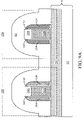
- a first exemplary structure according to a first embodiment of the present invention comprises a semiconductor substrate 8 containing a handle substrate 10 and an insulator layer 20 .
- a first fin cap 34 A and a second fin cap 34 B are present on top surfaces of the first semiconductor fin 32 A and the second semiconductor fin 32 B, respectively.
- a first semiconductor fin 32 A and a second semiconductor fin 32 B are formed on the insulator layer 20 in a first device region 100 and in a second device region 200 , respectively, by methods known in the art.
- a semiconductor-on-insulator (SOI) substrate containing the handle substrate 10 , a buried insulator layer which is the insulator layer 20 , and a semiconductor containing layer (not shown) having the same thickness as the height of the first and second semiconductor fins ( 32 A, 32 B) may be employed.
- a dielectric layer (not shown) having the same composition as the first and second fin caps ( 34 A, 34 B) is formed on the SOI substrate, followed by patterning of the dielectric layer and the semiconductor containing layer to form the first and second semiconductor fins ( 32 A, 32 B) and the first and second fin caps ( 34 A, 34 B).
- the first semiconductor fin 32 A and the second semiconductor fin 32 B comprise a semiconductor material such as silicon, germanium, a silicon germanium alloy, a silicon carbon alloy, a III-V compound semiconductor, or a II-VI compound semiconductor.
- the height of the first and second semiconductor fins ( 32 A, 32 B) may be from about 30 nm to about 300 nm, and typically from about 50 nm to about 200 nm, although lesser and greater heights are also contemplated herein.
- the first and second gate cap dielectric ( 34 A, 34 B) comprises a dielectric material such as a dielectric oxide or a dielectric nitride.
- the first and second gate cap dielectric ( 34 A, 3 B) may comprise silicon nitride.
- a first high-k gate dielectric layer 41 and a first metal gate layer 43 are formed on the first and second semiconductor fins ( 32 A, 32 B) and on the insulator layer 20 .
- the first high-k gate dielectric layer 41 comprises a first high-k dielectric material, which comprises a dielectric metal oxide having a dielectric constant that is greater than the dielectric constant of silicon oxide of 3.9.
- the dielectric metal oxide is a high-k material containing a metal and oxygen.
- the first high-k dielectric material may comprise HfO 2 , ZrO 2 , La 2 O 3 , Al 2 O 3 , TiO 2 , SrTiO 3 , LaAlO 3 , Y 2 O 3 , an alloy thereof, and a silicate thereof.
- the high-k gate dielectric layer 41 is formed by methods well known in the art including, for example, a chemical vapor deposition (CVD), an atomic layer deposition (ALD), molecular beam epitaxy (MBE), pulsed laser deposition (PLD), liquid source misted chemical deposition (LSMCD), etc.
- the thickness of the first high-k gate dielectric layer 41 may be from about 1.2 nm to about 6 nm, and may have an effective oxide thickness on the order of or less than 1 nm.
- the first metal gate layer 43 is formed directly on the first high-k gate dielectric layer 41 , for example, by chemical vapor deposition (CVD), physical vapor deposition (PVD), atomic layer deposition (ALD), etc.
- the first metal gate layer 43 comprises a first conductive metallic material which may be a metal, a metal alloy, or a metal nitride.
- the first metal gate layer 43 may comprise a material such as TaN, TiN, WN, TiAlN, TaCN, other conductive refractory metal nitride, or an alloy thereof.
- the thickness of the first metal gate layer 43 may be from about 5 nm to about 40 nm, and preferably from about 7 nm to about 20 nm, although lesser and greater thicknesses are also contemplated herein.
- the composition of the first metal gate layer 43 may be selected to optimize threshold voltages of a first finFET to be subsequently formed in the first device region 100 .
- an anisotropic reactive ion etch is performed on the first metal gate layer 43 to form a first metal gate ring 44 on the first semiconductor fin 32 A in the first device region 100 and another first metal gate ring 44 ′ on the second semiconductor fin 32 B in the second device region 200 .
- the anisotropic reactive ion etch may, or may not, be selective to the first high-k gate dielectric layer 43 .
- the first metal gate rings ( 44 , 44 ′) surround and laterally abut the first high-k gate dielectric layer 41 (See FIG. 2A ).
- Exposed portions of the first high-k gate dielectric layer 41 are etched, for example, by a substantially isotropic dry etch or a wet etch.
- a first high-k gate dielectric ring 42 is formed from a remaining portion of the first high-k gate dielectric layer 41 in the first device region 100
- another first high-k gate dielectric ring 42 ′ is formed from another remaining portion of the first high-k gate dielectric layer 41 in the second device region 200 .
- Each of the first high-k gate dielectric rings ( 42 , 42 ′) laterally abuts sidewalls of the first or second semiconductor fin ( 32 A or 32 B) and sidewalls of the first or second fin caps ( 34 A or 34 B).
- each of the first gate dielectric rings ( 42 , 42 ′) vertically abuts the insulator layer 20 .
- each of the first gate dielectric rings ( 42 , 42 ′) has an L-shaped vertical cross-sectional area, and has a shape that is topologically homeomorphic to a torus, i.e., forms a ring that encircles one of the first semiconductor fin 32 A and the second semiconductor fin 32 B.
- Each of the first metal gate rings ( 44 , 44 ′) laterally abuts outer sidewalls of one of the first high-k gate dielectric rings ( 42 , 42 ′), vertically abuts a top surface of a laterally protruding bottom portion of one of the first high-k gate dielectric rings ( 42 , 42 ′), and has a shape that is topologically homeomorphic to a torus, i.e., forms another ring that encircles one of the first semiconductor fin 32 A and the second semiconductor fin 32 B.
- a first photoresist 47 and a first block mask are employed to mask the first device region 100 , while exposing the second device region 200 using lithographic techniques known in the art.
- the another first metal gate ring 44 ′ and the another first high-k gate dielectric ring 42 ′ surrounding the second semiconductor fin 32 B are removed by an etch, which may be a substantially isotropic dry etch, wet etch, or a combination of both. Use of an anisotropic etch is also contemplated herein.
- the first photoresist 47 is subsequently removed.
- a second high-k gate dielectric layer 51 and a second metal gate layer 53 are formed on the outer sidewalls of the first metal gate ring 44 , exposed areas of the first high-k gate dielectric ring 42 , a first fin cap 34 A, a second fin cap 34 B, sidewalls of the second semiconductor fin 32 B, and the insulator layer 20 .
- the second high-k gate dielectric layer 51 comprises a second high-k dielectric material, which has the same compositional and physical characteristics as the first high-k dielectric material.
- the second high-k dielectric material may be the same as, or different from, the first high-k dielectric material.
- the first high-k dielectric material is optimized for one type of finFET, e.g., a p-type finFET or an n-type finFET, and the second high-k dielectric material is optimized for the opposite type of finFET.
- the thickness of the second high-k gate dielectric layer 51 is in the same range as the thickness of the first high-k gate dielectric layer 41 .
- the second metal gate layer 53 is formed directly on the second high-k gate dielectric layer 51 .
- the second metal gate layer 53 comprises a second conductive metallic material, which has the same compositional and physical characteristics as the first conductive metallic material.
- the second conductive metallic material may be the same as, or different from, the first conductive metallic material.
- the composition of the second metal gate layer 43 may be selected to optimize threshold voltages of a second finFET to be subsequently formed in the second device region 200 .
- an anisotropic reactive ion etch is performed on the second metal gate layer 53 to form a second metal gate ring 54 on the second semiconductor fin 32 B in the first device region 200 and another second metal gate ring 54 ′ on the first semiconductor fin 32 A in the first device region 100 .
- the anisotropic reactive ion etch is selective to the second high-k gate dielectric layer 51 .
- the second metal gate rings ( 54 , 54 ′) surround and laterally abut the second high-k gate dielectric layer 51 .
- a second photoresist 57 and a second block mask are employed to mask the second device region 200 , while exposing the first device region 100 using lithographic techniques known in the art.
- the another second metal gate ring 54 ′ surrounding the first semiconductor fin 32 A is then removed by an etch, which may be a substantially isotropic dry etch, wet etch, or a combination of both. Use of an anisotropic etch is also contemplated herein.
- the second photoresist 57 is removed, for example, by ashing.
- exposed portions of the second high-k gate dielectric layer 51 are etched, for example, by a substantially isotropic dry etch or a wet etch, which is selective to the first metal gate ring 44 and the second metal gate ring 54 .
- a second high-k gate dielectric ring 52 is formed from a remaining portion of the second high-k gate dielectric layer 51 in the second device region 200 .
- the second high-k gate dielectric ring 52 in the second device region 200 laterally abuts sidewalls of the second semiconductor fin 32 B and sidewalls of the second fin cap 34 B.
- the second gate dielectric ring 52 has an L-shaped vertical cross-sectional area, and has a shape that is topologically homeomorphic to a torus, i.e., forms a ring that encircles the second semiconductor fin 32 B. A suitable surface clean is performed as needed.
- the second metal gate ring 54 in the second device region 200 laterally abuts outer sidewalls of the second high-k gate dielectric ring 54 in the second device region 200 , vertically abuts a top surface of a laterally protruding bottom portion of the second high-k gate dielectric ring 54 in the second device region 200 , and has a shape that is topologically homeomorphic to a torus, i.e., forms another ring that encircles the second semiconductor fin 32 B.
- a silicon containing layer (not shown) is deposited on the first metal gate ring 44 (See FIG. 8A ), the second metal gate ring 54 (See FIG. 8A ), the first fin cap 34 A (See FIG. 8A ), the second fin cap 34 B (See FIG. 8A ), and the insulator layer 20 , for example, by chemical vapor deposition (CVD) such as low pressure chemical vapor deposition (LPCVD) or rapid thermal chemical vapor deposition (RTCVD).
- CVD chemical vapor deposition
- LPCVD low pressure chemical vapor deposition
- RTCVD rapid thermal chemical vapor deposition
- the silicon containing layer contains silicon, and may, or may not, comprise additional elements such as germanium and/or carbon.
- the silicon containing layer is preferably doped with dopants to enhance conductivity.
- the doping of the silicon containing layer is locally optimized for performance of the first finFET to be formed in the first device region 100 and the second finFET to be formed in the second device region 200 .
- the silicon containing layer 80 may be doped with p-type dopants directly over a p-type finFET, and doped with n-type dopants directly over an n-type finFET.
- the silicon containing gate line 80 is formed by lithographically pattering the silicon containing layer employing techniques known in the art.
- the silicon containing gate line 80 intersects the first and second semiconductor fins ( 32 A, 32 B) in a top-down view.
- another etch which may be a reactive ion etch, removes exposed portions of the first metal gate ring 44 (See FIG. 8A ), second metal gate ring 54 (See FIG. 8A ), the first high-k gate dielectric ring 42 (See FIG. 8A ), and the first metal gate ring 44 (See FIG. 8A ) from outside the area covered by the silicon containing gate line 80 in the top-down view.
- Two remaining disjoined portions of the first metal gate ring 44 constitute a first metal gate 144 .
- Two remaining disjoined portions of the second metal gate ring 54 constitute a second metal gate 154 .
- a portion of the silicon containing gate line 80 in the first device region 100 and the first metal gate 144 collectively constitute a first gate electrode controlling a current flow in the first semiconductor fin 32 A.
- Another portion of the silicon containing gate line 80 in the second device region 200 and the second metal gate 154 collectively constitute a second gate electrode controlling a current flow in the second semiconductor fin 32 B.
- Two remaining disjoined portions of the first high-k gate dielectric layer 42 comprise a first high-k gate dielectric 142 electrically separating a channel of the first semiconductor fin 32 A from the first gate electrode.
- the channel of the of the first semiconductor fin 32 A include the area of the first semiconductor fin 32 A shown in FIG. 9A .
- two remaining disjoined portions of the second high-k gate dielectric layer 52 comprise a second high-k gate dielectric 152 electrically separating a channel of the second semiconductor fin 32 B from the second gate electrode.
- the channel of the of the second semiconductor fin 32 B include the area of the second semiconductor fin 32 B shown in FIG. 9A .
- the exposed portions of the first and second semiconductor fins ( 32 A, 32 B) may be doped to form source and drain regions as known in the art. Formation of metal semiconductor alloys, such as metal silicides, may be performed, followed by deposition of middle-of-line dielectric material and formation of contacts to the various components in and on the first and second semiconductor fins ( 32 A, 32 B) to form a first finFET in the first device region 100 and a second finFET in the second device region 200 .
- the first finFET and the second finFET are of opposite conductivity types.
- the first high-k dielectric material and the second high-k dielectric material may be selected independent of each other.
- the first conductive metallic material and the second conductive metallic material may be selected independent of etch other.
- the first exemplary further provides a gate wiring located between the first device region 100 and the second device region 200 and containing yet another portion of the silicon containing gate liner 80 which vertically abuts the insulator layer 20 .
- High-k gate dielectric materials are not present in the gate wiring.
- a second exemplary semiconductor structure according to a second embodiment of the present invention is derived from the first exemplary semiconductor of FIGS. 2A and 2B by forming first fin spacers 62 on outer sidewalls of the first metal gate layer 43 in the first device region 100 and the second device region 200 .
- the first fin spacers 62 are formed by a substantially conformal deposition of a layer followed by an anisotropic reactive ion etch.
- the first fin spacers 62 may comprise a conductive material, a semiconductor material, or a dielectric material.
- the first fin spacers 62 may comprise polysilicon, silicon oxide, or silicon nitride.
- Each of the first fin spacers 62 has a shape that is topologically homeomorphic to a torus, i.e., forms a ring that encircles one of the first semiconductor fin 32 A and the second semiconductor fin 32 B.
- a block level photoresist 67 is applied and patterned to mask the first device region 100 , while exposing the second device region 200 using lithographic techniques known in the art.
- the exposed first fin spacer 62 located in the second device region 200 is removed by an etch, which may be a substantially isotropic dry etch, wet etch, or a combination of both. Use of an anisotropic etch is also contemplated herein.
- exposed portions of the first metal gate layer 43 are removed by an etch.
- the etch is a substantially isotropic etch such as a chemical dry etch or a wet etch. Use of an anisotropic etch is also contemplated herein.
- the etch is selective to the first high-k gate dielectric layer 41 .
- the remaining portion of the first metal gate layer 42 constitutes a first metal gate ring 46 . Due to the first fin spacer 62 on the first semiconductor fin 32 A, a “foot,” or a laterally protruding portion at a bottom, is formed on the first metal gate ring 46 .
- the first metal gate ring 46 laterally abuts outer sidewalls of the portion of the first high-k gate dielectric layer 41 on the first semiconductor fin 32 A. Further, the first metal gate ring 46 has an L-shaped vertical cross-sectional area, and has a shape that is topologically homeomorphic to a torus, i.e., forms a ring that encircles the first semiconductor fin 32 A.
- the first fin spacer 62 is removed by an etch, which may be a substantially isotropic etch, that is selective to the first high-k gate dielectric layer 41 and the first metal gate ring 46 .
- a suitable surface clean may be performed at this step.
- a second metal gate layer 53 is formed on the first high-k gate dielectric layer 41 and the first metal gate ring 46 .
- the composition and thickness of the second metal gate layer 53 may be the same as in the first embodiment.
- a silicon containing layer (not shown) having the same composition as in the first embodiment is deposited on the second metal gate layer 53 (See FIG. 14A ) employing the same methods as in the first embodiment.
- the silicon containing gate line 80 is formed by lithographically pattering the silicon containing layer employing techniques known in the art.
- the silicon containing gate line 80 intersects the first and second semiconductor fins ( 32 A, 32 B) in a top-down view.
- another etch which may be a reactive ion etch, removes exposed portions of the second metal gate layer 53 , the first metal gate ring 46 (See FIG. 14A ), and the first high-k gate dielectric layer 41 (See FIG. 8A ) from outside the area covered by the silicon containing gate line 80 in a top-down view.
- first metal gate 144 Two remaining disjoined portions of the first metal gate ring 44 constitute a first metal gate 144 .
- a portion of the silicon containing gate line 80 in the first device region 100 , a portion of the second metal gate layer 53 in the first device region 100 , and the first metal gate 144 collectively constitute a first gate electrode controlling a current flow in the first semiconductor fin 32 A.
- Another portion of the silicon containing gate line 80 in the second device region 200 and another portion of the second metal gate layer 53 in the second device region 200 collectively constitute a second gate electrode controlling a current flow in the second semiconductor fin 32 B.
- first finFET and the second finFET are of opposite conductivity types.
- Only one high-k gate dielectric layer, i.e., the first high-k gate dielectric layer 41 is employed in the second exemplary semiconductor structure.
- the first conductive metallic material and the second conductive metallic material may be selected independent of etch other as in the first embodiment.
- a third exemplary semiconductor structure according to a third embodiment of the present invention is derived the second semiconductor structure of FIGS. 13A and 13B by removing exposed portions of the first high-k electric layer 41 , for example, by a substantially isotropic etch.
- the substantially isotropic etch may be a chemical dry etch or a wet etch. Use of a reactive ion etch is also contemplated herein.
- a second high-k gate dielectric layer 51 is formed directly on sidewalls of the second semiconductor fin 32 B, the second fin cap 34 B, the first metal gate ring 46 , a top surface of the first fin cap 34 A, exposed portions of the first high-k gate dielectric ring 42 , and the insulator layer 20 .
- a second metal gate layer 53 is formed directly on the second high-k gate dielectric layer 51 .
- the second high-k gate dielectric layer 51 and the second metal gate layer 53 have the same composition and thickness as in the first embodiment.
- an anisotropic reactive ion etch is performed on the second metal gate layer 53 to form a second metal gate ring 54 on the second semiconductor fin 32 B in the first device region 200 and another second metal gate ring 54 ′ on the first semiconductor fin 32 A in the first device region 100 .
- the anisotropic reactive ion etch may, or may not, be selective to the second high-k gate dielectric layer 51 .
- the second metal gate rings ( 54 , 54 ′) surround and laterally abut the second high-k gate dielectric layer 51 .
- a second photoresist 57 and a second block mask are employed to mask the second device region 200 , while exposing the first device region 100 using lithographic techniques known in the art.
- the another second metal gate ring 54 ′ surrounding the first semiconductor fin 32 A are removed by an etch, which may be a substantially isotropic dry etch, wet etch, or a combination of both. Use of an anisotropic etch is also contemplated herein. The etch may, or may not, be selective to the second high-k gate dielectric layer 51 .
- the second photoresist 57 is subsequently removed. A suitable surface clean is performed as needed.
- any remaining exposed portions of the second high-k gate dielectric layer 51 are removed by an etch, which may be a substantially isotropic dry etch, wet etch, or a combination of both.
- a second high-k gate dielectric ring 52 is formed from a remaining portion of the second high-k gate dielectric layer 51 in the second device region 200 .
- the second high-k gate dielectric ring 52 in the second device region 200 laterally abuts sidewalls of the second semiconductor fin 32 B and sidewalls of the second fin cap 34 B. Further, the second gate dielectric rings 52 vertically abuts the insulator layer 20 .
- the second gate dielectric rings 52 has an L-shaped vertical cross-sectional area, and has a shape that is topologically homeomorphic to a torus, i.e., forms a ring that encircles the second semiconductor fin 32 B.
- the second metal gate ring 54 in the second device region 200 laterally abuts outer sidewalls of the second high-k gate dielectric ring 54 , vertically abuts a top surface of a laterally protruding bottom portion of the second high-k gate dielectric ring 54 , and has a shape that is topologically homeomorphic to a torus, i.e., forms another ring that encircles the second semiconductor fin 32 B.
- a silicon containing layer (not shown) is deposited and lithographically patterned as in the first embodiment to form a silicon containing gate line 80 .
- the composition of the silicon containing layer and the silicon containing gate line 80 may be the same as in the first embodiment.
- the silicon containing gate line 80 intersects the first and second semiconductor fins ( 32 A, 32 B) in a top-down view as in the first embodiment. Exposed portions of the first metal gate ring 44 (See FIG. 20A ), the second metal gate ring 54 (See FIG. 20A ), the first high-k gate dielectric ring 42 (See FIG. 20A ), and the second high-k gate dielectric ring 52 (See FIG. 20A ) are removed from outside the area covered by the silicon containing gate line 80 in the top-down view as in the first embodiment.
- first metal gate 146 Two remaining disjoined portions of the first metal gate ring 46 constitute a first metal gate 146 , which has an L-shaped vertical cross-sectional area.
- a second metal gate 154 , a first high-k gate dielectric 142 , and a second high-k gate dielectric 152 are formed as in the first embodiment.
- the rest of the processing sequence for forming a first finFET in the first device region 100 and a second finFET in the second device region 200 is the same as in the first embodiment.
- the first finFET and the second finFET are of opposite conductivity types.
- the third exemplary semiconductor structure allows independent selection of the first high-k dielectric material and the second high-k dielectric material to optimized performance of the first and second finFETs.
- the third exemplary semiconductor structure allows independent selection of the first conductive metallic material and the second conductive metallic material to optimized performance of the first and second finFETs.
- the third exemplary further provides a gate wiring located between the first device region 100 and the second device region 200 and containing yet another portion of the silicon containing gate liner 80 which vertically abuts the insulator layer 20 . High-k gate dielectric materials are not present in the gate wiring.
- a fourth exemplary semiconductor structure according to a fourth embodiment of the present invention is derived from the second semiconductor structure of FIGS. 12A and 12B by removing exposed portions of the first high-k gate dielectric layer 42 by an etch.
- the etch may be a substantially isotropic etch such as a chemical dry etch or a wet etch. Use of a reactive ion etch is also contemplated herein.
- the etch forms a first high-k gate dielectric ring 42 from a remaining portion of the first high-k gate dielectric layer 41 in the first device region 100 .
- the first high-k gate dielectric ring 42 laterally abuts sidewalls of the first semiconductor fin 32 A and sidewalls of the first fin cap 34 A. Further, the first gate dielectric ring 42 vertically abuts the insulator layer 20 .
- the first gate dielectric ring 42 has an L-shaped vertical cross-sectional area, and has a shape that is topologically homeomorphic to a torus, i.e., forms a ring that encircles the first semiconductor fin 32 A.
- the first metal gate ring 46 laterally abuts outer sidewalls of one of the first high-k gate dielectric ring 42 , vertically abuts a top surface of a laterally protruding bottom portion of the first high-k gate dielectric ring 42 , has another L-shaped cross-sectional area, and has a shape that is topologically homeomorphic to a torus, i.e., forms another ring that encircles the first semiconductor fin 32 A.
- a second high-k gate dielectric layer 51 is formed directly on sidewalls of the second semiconductor fin 32 B, the second fin cap 34 B, the first metal gate ring 46 , the first fin spacer 62 , a top surface of the first fin cap 34 A, exposed portions of the first high-k gate dielectric ring 42 , and the insulator layer 20 .
- a second metal gate layer 53 is formed directly on the second high-k gate dielectric layer 51 .
- the second high-k gate dielectric layer 51 and the second metal gate layer 53 have the same composition and thickness as in the first embodiment.
- a second fin spacer 72 is formed on outer sidewalls of the second metal gate layer 53 in the second device region 200
- another second fin spacer 72 ′ is formed on outer sidewalls of the second metal gate layer 53 in the first device region 100 by a substantially conformal deposition of a layer followed by an anisotropic reactive ion etch.
- the second fin spacer 72 in the second device region 200 and the another second fin spacer 72 ′ in the first device region 100 may comprise a conductive material, a semiconductor material, or a dielectric material as the first fin spacers 62 in the first embodiment.
- the second fin spacers ( 72 , 72 ′) in the first and second device regions ( 100 , 200 ) may comprise polysilicon, silicon oxide, or silicon nitride.
- Each of the second fin spacer 72 in the second device region 200 and the another second fin spacer 72 ′ in the first device region 100 has a shape that is topologically homeomorphic to a torus, i.e., forms a ring that encircles one of the first semiconductor fin 32 A and the second semiconductor fin 32 B.
- a second photoresist 57 is applied and patterned to mask the second device region 200 , while exposing the first device region 100 using lithographic techniques known in the art.
- the another second fin spacer 72 ′ located in the first device region 100 is removed by an etch, which may be a substantially isotropic dry etch, wet etch, or a combination of both. Use of an anisotropic etch is also contemplated herein.
- the second photoresist 57 is subsequently removed.
- exposed portions of the second metal gate layer 51 are removed by an etch.
- the etch may be a substantially isotropic etch such as a dry etch or a wet etch.
- the etch may, or may not, be selective to the second high-k gate dielectric layer 51 .
- Use of an anisotropic reactive ion etch for removal of exposed portions of the second metal gate layer 51 is also contemplated herein.
- Exposed portions of the second high-k gate dielectric layer 51 is thereafter removed by another etch, which may be another substantially isotropic etch.
- the etch employed to remove the second high-k gate dielectric layer 51 is selective to the underlying layers.
- the two etches form a second high-k gate dielectric ring 52 from a remaining portion of the second high-k gate dielectric layer 51 in the second device region 200 .
- the second high-k gate dielectric ring 52 laterally abuts sidewalls of the second semiconductor fin 32 B and sidewalls of the second fin cap 34 B. Further, the second gate dielectric ring 52 vertically abuts the insulator layer 20 .
- the second gate dielectric ring 52 has an L-shaped vertical cross-sectional area, and has a shape that is topologically homeomorphic to a torus, i.e., forms a ring that encircles the second semiconductor fin 32 B.
- the second metal gate ring 56 laterally abuts outer sidewalls of the second high-k gate dielectric ring 52 , vertically abuts a top surface of a laterally protruding bottom portion of the second high-k gate dielectric ring 52 , has another L-shaped cross-sectional area, and has a shape that is topologically homeomorphic to a torus, i.e., forms another ring that encircles the second semiconductor fin 32 B.
- a silicon containing layer (not shown) is deposited and lithographically patterned as in the first embodiment to form a silicon containing gate line 80 .
- the composition of the silicon containing layer and the silicon containing gate line 80 may be the same as in the first embodiment.
- the silicon containing gate line 80 intersects the first and second semiconductor fins ( 32 A, 32 B) in a top-down view as in the first embodiment. Exposed portions of the first fin spacer 62 , the second fin spacer 72 , the first metal gate ring 46 (See FIG. 26A ), the second metal gate ring 56 (See FIG. 26A ), the first high-k gate dielectric ring 42 (See FIG. 26A ), and the second high-k gate dielectric ring 52 (See FIG. 26A ) are removed from outside the area covered by the silicon containing gate line 80 in the top-down view as in the first embodiment.
- first metal gate 146 Two remaining disjoined portions of the first metal gate ring 46 constitute a first metal gate 146 , which has an L-shaped vertical cross-sectional area.
- second metal gate 156 Two remaining disjoined portions of the second metal gate ring 56 constitute a second metal gate 156 , which has an L-shaped vertical cross-sectional area.
- a first high-k gate dielectric 142 , and a second high-k gate dielectric 152 are formed as in the first embodiment.
- the rest of the processing sequence for forming a first finFET in the first device region 100 and a second finFET in the second device region 200 is the same as in the first embodiment.
- the first finFET and the second finFET are of opposite conductivity types.
- the fourth exemplary semiconductor structure allows independent selection of the first high-k dielectric material and the second high-k dielectric material to optimized performance of the first and second finFETs. Also, the fourth exemplary semiconductor structure allows independent selection of the first conductive metallic material and the second conductive metallic material to optimized performance of the first and second finFETs. As in the first embodiment, the fourth exemplary further provides a gate wiring located between the first device region 100 and the second device region 200 and containing yet another portion of the silicon containing gate liner 80 which vertically abuts the insulator layer 20 . High-k gate dielectric materials are not present in the gate wiring.
Abstract
Description
Claims (12)
Priority Applications (1)
| Application Number | Priority Date | Filing Date | Title |
|---|---|---|---|
| US11/860,840 US7659157B2 (en) | 2007-09-25 | 2007-09-25 | Dual metal gate finFETs with single or dual high-K gate dielectric |
Applications Claiming Priority (1)
| Application Number | Priority Date | Filing Date | Title |
|---|---|---|---|
| US11/860,840 US7659157B2 (en) | 2007-09-25 | 2007-09-25 | Dual metal gate finFETs with single or dual high-K gate dielectric |
Publications (2)
| Publication Number | Publication Date |
|---|---|
| US20090078997A1 US20090078997A1 (en) | 2009-03-26 |
| US7659157B2 true US7659157B2 (en) | 2010-02-09 |
Family
ID=40470715
Family Applications (1)
| Application Number | Title | Priority Date | Filing Date |
|---|---|---|---|
| US11/860,840 Expired - Fee Related US7659157B2 (en) | 2007-09-25 | 2007-09-25 | Dual metal gate finFETs with single or dual high-K gate dielectric |
Country Status (1)
| Country | Link |
|---|---|
| US (1) | US7659157B2 (en) |
Cited By (12)
| Publication number | Priority date | Publication date | Assignee | Title |
|---|---|---|---|---|
| US20120280330A1 (en) * | 2011-05-06 | 2012-11-08 | Samsung Electronics Co., Ltd. | Semiconductor devices and methods for fabricating the same |
| US20130154002A1 (en) * | 2011-12-16 | 2013-06-20 | Taiwan Semiconductor Manufacturing Company, Ltd. | FinFETs with Multiple Threshold Voltages |
| US20130316503A1 (en) * | 2012-05-23 | 2013-11-28 | International Business Machines Corporation | STRUCTURE AND METHOD TO MODULATE THRESHOLD VOLTAGE FOR HIGH-K METAL GATE FIELD EFFECT TRANSISTORS (FETs) |
| US8859355B1 (en) | 2013-05-06 | 2014-10-14 | International Business Machines Corporation | Method to make dual material finFET on same substrate |
| US8951884B1 (en) | 2013-11-14 | 2015-02-10 | United Microelectronics Corp. | Method for forming a FinFET structure |
| US9006094B2 (en) | 2012-04-18 | 2015-04-14 | International Business Machines Corporation | Stratified gate dielectric stack for gate dielectric leakage reduction |
| US9059217B2 (en) | 2013-03-28 | 2015-06-16 | International Business Machines Corporation | FET semiconductor device with low resistance and enhanced metal fill |
| US9412664B2 (en) | 2013-05-06 | 2016-08-09 | International Business Machines Corporation | Dual material finFET on single substrate |
| US9685526B2 (en) | 2014-02-12 | 2017-06-20 | International Business Machines Corporation | Side gate assist in metal gate first process |
| US10043807B1 (en) * | 2017-05-24 | 2018-08-07 | United Microelectronics Corp. | Semiconductor device and method of forming the same |
| US20180350800A1 (en) * | 2016-11-29 | 2018-12-06 | Taiwan Semiconductor Manufacturing Co., Ltd. | Semiconductor device and manufacturing method thereof |
| US11011626B2 (en) | 2019-05-07 | 2021-05-18 | International Business Machines Corporation | Fin field-effect transistor with reduced parasitic capacitance and reduced variability |
Families Citing this family (24)
| Publication number | Priority date | Publication date | Assignee | Title |
|---|---|---|---|---|
| US7825437B2 (en) * | 2007-12-28 | 2010-11-02 | Intel Corporation | Unity beta ratio tri-gate transistor static random access memory (SRAM) |
| US7867835B2 (en) * | 2008-02-29 | 2011-01-11 | Chartered Semiconductor Manufacturing Ltd. | Integrated circuit system for suppressing short channel effects |
| US8110877B2 (en) * | 2008-12-19 | 2012-02-07 | Intel Corporation | Metal-insulator-semiconductor tunneling contacts having an insulative layer disposed between source/drain contacts and source/drain regions |
| US8202780B2 (en) * | 2009-07-31 | 2012-06-19 | International Business Machines Corporation | Method for manufacturing a FinFET device comprising a mask to define a gate perimeter and another mask to define fin regions |
| CN102420232B (en) * | 2010-09-28 | 2014-08-13 | 中国科学院微电子研究所 | Flash memory device and formation method thereof |
| CN102655168A (en) * | 2011-03-04 | 2012-09-05 | 中国科学院微电子研究所 | Gate structure and manufacturing method thereof |
| US8697522B2 (en) * | 2011-07-05 | 2014-04-15 | International Business Machines Corporation | Bulk finFET with uniform height and bottom isolation |
| US8698199B2 (en) * | 2012-01-11 | 2014-04-15 | United Microelectronics Corp. | FinFET structure |
| CN103219366B (en) * | 2012-01-20 | 2017-09-05 | 联华电子股份有限公司 | Fin-shaped field-effect transistor structure and preparation method thereof |
| US9012975B2 (en) * | 2012-06-14 | 2015-04-21 | United Microelectronics Corp. | Field effect transistor and manufacturing method thereof |
| US8981481B2 (en) | 2012-06-28 | 2015-03-17 | Intel Corporation | High voltage three-dimensional devices having dielectric liners |
| US8941156B2 (en) * | 2013-01-07 | 2015-01-27 | International Business Machines Corporation | Self-aligned dielectric isolation for FinFET devices |
| US9006087B2 (en) | 2013-02-07 | 2015-04-14 | International Business Machines Corporation | Diode structure and method for wire-last nanomesh technologies |
| US20140315371A1 (en) * | 2013-04-17 | 2014-10-23 | International Business Machines Corporation | Methods of forming isolation regions for bulk finfet semiconductor devices |
| US20150221726A1 (en) * | 2014-02-04 | 2015-08-06 | Globalfoundries Inc. | Finfet with isolated source and drain |
| US9281192B2 (en) * | 2014-03-13 | 2016-03-08 | Taiwan Semiconductor Manufacturing Co., Ltd. | CMP-friendly coatings for planar recessing or removing of variable-height layers |
| CN105336772B (en) * | 2014-05-26 | 2021-11-30 | 中芯国际集成电路制造(上海)有限公司 | Fin type TFET (thin film transistor) and manufacturing method thereof |
| US9922880B2 (en) * | 2014-09-26 | 2018-03-20 | Qualcomm Incorporated | Method and apparatus of multi threshold voltage CMOS |
| US9449972B1 (en) | 2015-03-06 | 2016-09-20 | Globalfoundries Inc. | Ferroelectric FinFET |
| CN107799593B (en) * | 2016-09-07 | 2020-06-05 | 中芯国际集成电路制造(上海)有限公司 | Vertical FinFET device, preparation method thereof and electronic device |
| US10903336B2 (en) * | 2017-11-28 | 2021-01-26 | Taiwan Semiconductor Manufacturing Co., Ltd. | Semiconductor device and method of manufacturing the same |
| JP7034834B2 (en) * | 2018-05-30 | 2022-03-14 | ルネサスエレクトロニクス株式会社 | Semiconductor devices and their manufacturing methods |
| US10991689B2 (en) | 2019-04-05 | 2021-04-27 | Globalfoundries U.S. Inc. | Additional spacer for self-aligned contact for only high voltage FinFETs |
| US11450660B2 (en) * | 2020-04-27 | 2022-09-20 | Taiwan Semiconductor Manufacturing Company, Ltd. | Semiconductor device and method of fabricating the same |
Citations (2)
| Publication number | Priority date | Publication date | Assignee | Title |
|---|---|---|---|---|
| US20070128858A1 (en) * | 2005-12-05 | 2007-06-07 | Suvi Haukka | Method of producing thin films |
| US20090065870A1 (en) * | 2005-11-15 | 2009-03-12 | Hong-Jyh Li | Semiconductor Devices and Methods of Manufacture Thereof |
-
2007
- 2007-09-25 US US11/860,840 patent/US7659157B2/en not_active Expired - Fee Related
Patent Citations (2)
| Publication number | Priority date | Publication date | Assignee | Title |
|---|---|---|---|---|
| US20090065870A1 (en) * | 2005-11-15 | 2009-03-12 | Hong-Jyh Li | Semiconductor Devices and Methods of Manufacture Thereof |
| US20070128858A1 (en) * | 2005-12-05 | 2007-06-07 | Suvi Haukka | Method of producing thin films |
Cited By (29)
| Publication number | Priority date | Publication date | Assignee | Title |
|---|---|---|---|---|
| US20120280330A1 (en) * | 2011-05-06 | 2012-11-08 | Samsung Electronics Co., Ltd. | Semiconductor devices and methods for fabricating the same |
| US20130154002A1 (en) * | 2011-12-16 | 2013-06-20 | Taiwan Semiconductor Manufacturing Company, Ltd. | FinFETs with Multiple Threshold Voltages |
| US9472638B2 (en) * | 2011-12-16 | 2016-10-18 | Taiwan Semiconductor Manufacturing Company, Ltd. | FinFETs with multiple threshold voltages |
| US10020230B2 (en) * | 2011-12-16 | 2018-07-10 | Taiwan Semiconductor Manufacturing Company, Ltd. | FinFETs with multiple threshold voltages |
| US8907431B2 (en) * | 2011-12-16 | 2014-12-09 | Taiwan Semiconductor Manufacturing Company, Ltd. | FinFETs with multiple threshold voltages |
| US20140377944A1 (en) * | 2011-12-16 | 2014-12-25 | Taiwan Semiconductor Manufacturing Company, Ltd. | FinFETs with Multiple Threshold Voltages |
| US20170025312A1 (en) * | 2011-12-16 | 2017-01-26 | Taiwan Semiconductor Manufacturing Company, Ltd. | FinFETs with Multiple Threshold Voltages |
| US9123746B2 (en) * | 2011-12-16 | 2015-09-01 | Taiwan Semiconductor Manufacturing Company, Ltd. | FinFETs with multiple threshold voltages |
| US9385207B2 (en) | 2012-04-18 | 2016-07-05 | International Business Machines Corporation | Stratified gate dielectric stack for gate dielectric leakage reduction |
| US9627214B2 (en) | 2012-04-18 | 2017-04-18 | International Business Machines Corporation | Stratified gate dielectric stack for gate dielectric leakage reduction |
| US9006094B2 (en) | 2012-04-18 | 2015-04-14 | International Business Machines Corporation | Stratified gate dielectric stack for gate dielectric leakage reduction |
| US9514948B2 (en) | 2012-04-18 | 2016-12-06 | International Business Machines Corporation | Stratified gate dielectric stack for gate dielectric leakage reduction |
| US9041116B2 (en) * | 2012-05-23 | 2015-05-26 | International Business Machines Corporation | Structure and method to modulate threshold voltage for high-K metal gate field effect transistors (FETs) |
| US9214397B2 (en) * | 2012-05-23 | 2015-12-15 | Globalfoundries Inc. | Structure and method to modulate threshold voltage for high-K metal gate field effect transistors (FETs) |
| US20130316503A1 (en) * | 2012-05-23 | 2013-11-28 | International Business Machines Corporation | STRUCTURE AND METHOD TO MODULATE THRESHOLD VOLTAGE FOR HIGH-K METAL GATE FIELD EFFECT TRANSISTORS (FETs) |
| US9059217B2 (en) | 2013-03-28 | 2015-06-16 | International Business Machines Corporation | FET semiconductor device with low resistance and enhanced metal fill |
| US9412664B2 (en) | 2013-05-06 | 2016-08-09 | International Business Machines Corporation | Dual material finFET on single substrate |
| US9048318B2 (en) * | 2013-05-06 | 2015-06-02 | International Business Machines Corporation | Dual material finFET on same substrate |
| US9613963B2 (en) | 2013-05-06 | 2017-04-04 | International Business Machines Corporation | Dual material finFET on single substrate |
| US9640536B2 (en) | 2013-05-06 | 2017-05-02 | International Business Machines | Method to make dual material finFET on same substrate |
| US8859355B1 (en) | 2013-05-06 | 2014-10-14 | International Business Machines Corporation | Method to make dual material finFET on same substrate |
| US8951884B1 (en) | 2013-11-14 | 2015-02-10 | United Microelectronics Corp. | Method for forming a FinFET structure |
| US9685526B2 (en) | 2014-02-12 | 2017-06-20 | International Business Machines Corporation | Side gate assist in metal gate first process |
| US20180350800A1 (en) * | 2016-11-29 | 2018-12-06 | Taiwan Semiconductor Manufacturing Co., Ltd. | Semiconductor device and manufacturing method thereof |
| US10937783B2 (en) | 2016-11-29 | 2021-03-02 | Taiwan Semiconductor Manufacturing Co., Ltd. | Semiconductor device and manufacturing method thereof |
| US11043489B2 (en) * | 2016-11-29 | 2021-06-22 | Taiwan Semiconductor Manufacturing Co., Ltd. | Semiconductor device and manufacturing method thereof |
| US11728332B2 (en) | 2016-11-29 | 2023-08-15 | Taiwan Semiconductor Manufacturing Company, Ltd. | Semiconductor device and manufacturing method thereof |
| US10043807B1 (en) * | 2017-05-24 | 2018-08-07 | United Microelectronics Corp. | Semiconductor device and method of forming the same |
| US11011626B2 (en) | 2019-05-07 | 2021-05-18 | International Business Machines Corporation | Fin field-effect transistor with reduced parasitic capacitance and reduced variability |
Also Published As
| Publication number | Publication date |
|---|---|
| US20090078997A1 (en) | 2009-03-26 |
Similar Documents
| Publication | Publication Date | Title |
|---|---|---|
| US7659157B2 (en) | Dual metal gate finFETs with single or dual high-K gate dielectric | |
| US9514948B2 (en) | Stratified gate dielectric stack for gate dielectric leakage reduction | |
| US8030709B2 (en) | Metal gate stack and semiconductor gate stack for CMOS devices | |
| US9153657B2 (en) | Semiconductor devices comprising a fin | |
| CN107863299B (en) | FinFET and manufacturing method thereof | |
| US6919601B2 (en) | Semiconductor device with gate electrode formed on each of three side surfaces of an active layer, and manufacturing method thereof | |
| US8809176B2 (en) | Replacement gate with reduced gate leakage current | |
| US11139294B2 (en) | Semiconductor structure and fabrication method thereof | |
| KR20050094576A (en) | Three dimensional cmos field effect transistor and method of fabricating the same | |
| WO2012035679A1 (en) | Semiconductor device and manufacturing method therefor | |
| KR20080058341A (en) | Multiple low and high k gate oxides on single gate for lower miller capacitance and improved drive current | |
| KR20110107852A (en) | Spacer and gate dielectric structure for programmable high-k/metal gate memory transistors integrated with logic transistors and method of forming the same | |
| US11295988B2 (en) | Semiconductor FET device with bottom isolation and high-κ first | |
| TWI714583B (en) | Semiconductor device and method of forming the same | |
| CN103855010A (en) | Fin field effect transistor (FinFET) and manufacturing method thereof | |
| US20060170053A1 (en) | Accumulation mode multiple gate transistor | |
| US20110215405A1 (en) | Prevention of oxygen absorption into high-k gate dielectric of silicon-on-insulator based finfet devices | |
| CN103390637B (en) | FinFET and manufacture method thereof | |
| EP3719836A2 (en) | Semiconductor device and method for fabricating the same | |
| US11387317B2 (en) | Field-effect transistor without punch-through stopper and fabrication method thereof | |
| US8895403B2 (en) | Transistor, method for fabricating the transistor, and semiconductor device comprising the transistor | |
| US11302794B2 (en) | FinFET with dual work function metal | |
| US10930740B2 (en) | Multi-direction channel transistor and semiconductor device including the multi-direction channel transistor | |
| US20220328642A1 (en) | Semiconductor structure and forming method thereof | |
| US10388570B2 (en) | Substrate with a fin region comprising a stepped height structure |
Legal Events
| Date | Code | Title | Description |
|---|---|---|---|
| AS | Assignment |
Owner name: INTERNATIONAL BUSINESS MACHINES CORPORATION,NEW YO Free format text: ASSIGNMENT OF ASSIGNORS INTEREST;ASSIGNORS:GREENE, BRIAN J.;KUMAR, MAHENDER;SIGNING DATES FROM 20070924 TO 20070925;REEL/FRAME:019934/0896 Owner name: INTERNATIONAL BUSINESS MACHINES CORPORATION, NEW Y Free format text: ASSIGNMENT OF ASSIGNORS INTEREST;ASSIGNORS:GREENE, BRIAN J.;KUMAR, MAHENDER;REEL/FRAME:019934/0896;SIGNING DATES FROM 20070924 TO 20070925 |
|
| FEPP | Fee payment procedure |
Free format text: PAYOR NUMBER ASSIGNED (ORIGINAL EVENT CODE: ASPN); ENTITY STATUS OF PATENT OWNER: LARGE ENTITY |
|
| STCF | Information on status: patent grant |
Free format text: PATENTED CASE |
|
| REMI | Maintenance fee reminder mailed | ||
| FPAY | Fee payment |
Year of fee payment: 4 |
|
| SULP | Surcharge for late payment | ||
| AS | Assignment |
Owner name: GLOBALFOUNDRIES U.S. 2 LLC, NEW YORK Free format text: ASSIGNMENT OF ASSIGNORS INTEREST;ASSIGNOR:INTERNATIONAL BUSINESS MACHINES CORPORATION;REEL/FRAME:036550/0001 Effective date: 20150629 |
|
| AS | Assignment |
Owner name: GLOBALFOUNDRIES INC., CAYMAN ISLANDS Free format text: ASSIGNMENT OF ASSIGNORS INTEREST;ASSIGNORS:GLOBALFOUNDRIES U.S. 2 LLC;GLOBALFOUNDRIES U.S. INC.;REEL/FRAME:036779/0001 Effective date: 20150910 |
|
| AS | Assignment |
Owner name: AURIGA INNOVATIONS, INC., CANADA Free format text: ASSIGNMENT OF ASSIGNORS INTEREST;ASSIGNOR:GLOBALFOUNDRIES INC.;REEL/FRAME:041777/0233 Effective date: 20161207 |
|
| FPAY | Fee payment |
Year of fee payment: 8 |
|
| FEPP | Fee payment procedure |
Free format text: MAINTENANCE FEE REMINDER MAILED (ORIGINAL EVENT CODE: REM.); ENTITY STATUS OF PATENT OWNER: LARGE ENTITY |
|
| LAPS | Lapse for failure to pay maintenance fees |
Free format text: PATENT EXPIRED FOR FAILURE TO PAY MAINTENANCE FEES (ORIGINAL EVENT CODE: EXP.); ENTITY STATUS OF PATENT OWNER: LARGE ENTITY |
|
| STCH | Information on status: patent discontinuation |
Free format text: PATENT EXPIRED DUE TO NONPAYMENT OF MAINTENANCE FEES UNDER 37 CFR 1.362 |
|
| FP | Lapsed due to failure to pay maintenance fee |
Effective date: 20220209 |