US7656208B2 - PLL oscillation circuit - Google Patents
PLL oscillation circuit Download PDFInfo
- Publication number
- US7656208B2 US7656208B2 US11/812,520 US81252007A US7656208B2 US 7656208 B2 US7656208 B2 US 7656208B2 US 81252007 A US81252007 A US 81252007A US 7656208 B2 US7656208 B2 US 7656208B2
- Authority
- US
- United States
- Prior art keywords
- converter
- oscillation circuit
- narrow
- output
- crystal filter
- Prior art date
- Legal status (The legal status is an assumption and is not a legal conclusion. Google has not performed a legal analysis and makes no representation as to the accuracy of the status listed.)
- Expired - Fee Related, expires
Links
Images


Classifications
-
- H—ELECTRICITY
- H03—ELECTRONIC CIRCUITRY
- H03L—AUTOMATIC CONTROL, STARTING, SYNCHRONISATION OR STABILISATION OF GENERATORS OF ELECTRONIC OSCILLATIONS OR PULSES
- H03L7/00—Automatic control of frequency or phase; Synchronisation
- H03L7/06—Automatic control of frequency or phase; Synchronisation using a reference signal applied to a frequency- or phase-locked loop
- H03L7/16—Indirect frequency synthesis, i.e. generating a desired one of a number of predetermined frequencies using a frequency- or phase-locked loop
- H03L7/18—Indirect frequency synthesis, i.e. generating a desired one of a number of predetermined frequencies using a frequency- or phase-locked loop using a frequency divider or counter in the loop
-
- H—ELECTRICITY
- H03—ELECTRONIC CIRCUITRY
- H03L—AUTOMATIC CONTROL, STARTING, SYNCHRONISATION OR STABILISATION OF GENERATORS OF ELECTRONIC OSCILLATIONS OR PULSES
- H03L7/00—Automatic control of frequency or phase; Synchronisation
- H03L7/06—Automatic control of frequency or phase; Synchronisation using a reference signal applied to a frequency- or phase-locked loop
- H03L7/08—Details of the phase-locked loop
- H03L7/085—Details of the phase-locked loop concerning mainly the frequency- or phase-detection arrangement including the filtering or amplification of its output signal
Definitions
- the present invention relates to a PLL (Phase Locked Loop) oscillation circuit, and, more particularly, to a PLL oscillation circuit which prevents the phase noise characteristic and spurious characteristic of a VCO (Voltage Controlled Oscillator) output from being degraded.
- PLL Phase Locked Loop
- VCO Voltage Controlled Oscillator
- FIG. 10 is a configuration block diagram of the conventional digitally controlled PLL oscillation circuit.
- the conventional digitally controlled PLL oscillation circuit has a VCO 1 , a frequency divider 2 , a reference oscillation circuit 3 , an A/D (Analogue/Digital) converter 4 , a phase comparator 5 , a digital filter 6 , a D/A (Digital/Analogue) converter 7 , and an analog filter 8 .
- the VCO 1 is a voltage controlled oscillator that generates a desired frequency Fout in response to an input from the analog filter 8 as a control voltage.
- the frequency divider 2 divides the oscillation frequency Fout generated by the VCO 1 to 1/N, and sends the resultant frequency to the A/D converter 4 .
- the reference oscillation circuit 3 generates a reference signal (reference clock) Fref.
- the A/D converter 4 converts an analog signal from the frequency divider 2 to a digital signal according to the reference clock supplied from the reference oscillation circuit 3 .
- the phase comparator 5 compares the phase of the digital signal from the A/D converter 4 with the phase of the reference signal from the reference oscillation circuit 3 , and outputs a phase difference signal.
- the digital filter 6 filters the phase difference signal from the phase comparator 5 .
- the D/A converter 7 converts the digital signal from the digital filter 6 to an analog signal according to the reference clock supplied from the reference oscillation circuit 3 .
- the analog filter 8 smooths the analog signal from the D/A converter 7 , and outputs the analog signal as a control voltage to the VCO 1 .
- Japanese Patent Application Laid-Open No. 2004-253945 discloses a related art relating to a PLL circuit.
- the related art is a signal phase synchronization apparatus that stably extracts a clock with a less frequency variation from a PLL circuit using a bandpass filter (XBPF) comprising a crystal oscillator.
- XBPF bandpass filter
- the related art is premised on an analogously controlled PLL circuit and configured to allow a reproduction signal input to the phase comparator to pass the XBPF.
- the reference signal Fref is used in each of the A/D converter 4 , the phase comparator 5 and the D/A converter 7 . Because the reference signal Fref significantly influences the PLL performance, the reference signal Fref should desirably be stable free of noise, jitter or a spurious wave.
- the reference signal contains noise, jitter or a spurious wave, however, the phase noise characteristic and spurious characteristic of the output Fout of the VCO 1 would be degraded.
- the A/D converter 4 generates a digital signal to be subjected to phase comparison, and is likely to be influenced by the reference signal Fref, thereby significantly influencing the whole PLL oscillation circuit.
- the present invention has been made in consideration of the aforementioned situation, and it is an object of the invention to provide a PLL oscillation circuit capable of preventing the phase noise characteristic and spurious characteristic of a VCO output from being degraded.
- the first aspect of the invention is a digitally controlled PLL oscillation circuit including a voltage controlled oscillator; a frequency divider that divides an output from the voltage controlled oscillator; a reference oscillation circuit that generates a reference signal; an A/D converter that performs analog-to-digital conversion of an output from the frequency divider based on the reference signal; a phase comparator that compares a phase of an output from the A/D converter with a phase of the reference signal; a digital filter that filters an output from the phase comparator; a D/A converter that performs digital-to-analog conversion of an output from the digital filter based on the reference signal; an analog filter that smooths an output of the D/A converter and outputs as a control signal for the voltage controlled oscillator; and a first narrow-band crystal filter provided between the reference oscillation circuit and the A/D converter so that the reference signal to be supplied to the A/D converter from the reference oscillation circuit passes through the first narrow-band crystal filter.
- the PLL oscillation circuit can therefore
- a first amplifier is provided between the first narrow-band crystal filter and the A/D converter to amplify a signal from the first narrow-band crystal filter.
- the signal level is made lower by the crystal filter, therefore, the level can be amplified to an adequate level.
- a second narrow-band crystal filter is provided between the reference oscillation circuit and the phase comparator so that the reference signal to be supplied to the phase comparator from the reference oscillation circuit passes through the second narrow-band crystal filter.
- the PLL oscillation circuit can therefore cancel noise, jitter or a spurious wave contained in the reference signal, resulting in improvements of the phase noise characteristic and spurious characteristic of the output of the voltage controlled oscillator.
- a second amplifier is provided between the second narrow-band crystal filter and the phase comparator to amplify a signal from the second narrow-band crystal filter.
- the level can be amplified to an adequate level.
- a third narrow-band crystal filter is provided between the reference oscillation circuit and the D/A converter so that the reference signal to be supplied to the D/A converter from the reference oscillation circuit passes through the third narrow-band crystal filter.
- the PLL oscillation circuit can therefore cancel noise, jitter or a spurious wave contained in the reference signal, resulting in improvements of the phase noise characteristic and spurious characteristic of the output of the voltage controlled oscillator.
- a third amplifier is provided between the third narrow-band crystal filter and the D/A converter to amplify a signal from the third narrow-band crystal filter.
- the signal level is made lower by the crystal filter, therefore, the level can be amplified to an adequate level.
- the second aspect of the invention is a digitally controlled PLL oscillation circuit including a voltage controlled oscillator; a frequency divider that divides an output from the voltage controlled oscillator; a reference oscillation circuit that generates a reference signal; an A/D converter that performs analog-to-digital conversion of an output from the frequency divider based on the reference signal; a phase comparator that compares a phase of an output from the A/D converter with a phase of the reference signal; a digital filter that filters an output from the phase comparator; a D/A converter that performs digital-to-analog conversion of an output from the digital filter based on the reference signal; an analog filter that smooths an output of the D/A converter and outputs as a control signal for the voltage controlled oscillator; and a fourth narrow-band crystal filter provided at an output stage of the reference oscillation circuit so that the reference signal supplied from the reference oscillation circuit is output through the fourth narrow-band crystal filter to the A/D converter, the phase comparator and the D/A converter.
- the third aspect of the invention is a digitally controlled PLL oscillation circuit including a voltage controlled oscillator; a frequency divider that divides an output from the voltage controlled oscillator; a reference oscillation circuit that generates a reference signal; an A/D converter that performs analog-to-digital conversion of an output from the frequency divider based on the reference signal; a phase comparator that compares a phase of an output from the A/D converter with a phase of the reference signal; a digital filter that filters an output from the phase comparator; a D/A converter that performs digital-to-analog conversion of an output from the digital filter based on the reference signal; an analog filter that smooths an output of the D/A converter and outputs as a control signal for the voltage controlled oscillator; and a fifth narrow-band crystal filter and a fourth amplifier that are provided at an output stage of the reference oscillation circuit so that the reference signal supplied from the reference oscillation circuit passes through the fifth narrow-band crystal filter, is amplified by the fourth amplifier, and is output to
- the PLL oscillation circuit can therefore cancel noise, jitter or a spurious wave contained in the reference signal, resulting in improvements of the phase noise characteristic and spurious characteristic of the output of the voltage controlled oscillator and allowing the level to be amplified to an adequate level when the signal level is made lower by the crystal filter.
- FIG. 1 is a configuration block diagram of a PLL oscillation circuit according to a first embodiment of the present invention.
- FIG. 2 is a diagram showing the result of analyzing a digital signal output from an A/D converter when a reference frequency signal contains a spurious wave.
- FIG. 3 is a diagram showing the spurious characteristic of an output Fout when an MCF is not inserted.
- FIG. 4 is a diagram showing the transfer characteristic of an MCF inserted.
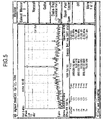
- FIG. 5 is a diagram showing the spurious characteristic of an output Fout when an MCF is inserted.
- FIG. 6 is a configuration block diagram of a PLL oscillation circuit according to a second embodiment of the invention.
- FIG. 7 is a configuration block diagram of a PLL oscillation circuit according to a third embodiment of the invention.
- FIG. 8 is a configuration block diagram of a PLL oscillation circuit according to a fourth embodiment of the invention.
- FIG. 9 is a configuration block diagram of a PLL oscillation circuit according to a fifth embodiment of the invention.
- FIG. 10 is a configuration block diagram of the conventional digitally controlled PLL oscillation circuit.
- a PLL oscillation circuit is a digitally controlled PLL oscillation circuit configured in such a way that a reference signal to be supplied to an A/D converter which performs A/D conversion of the output of a VCO is let to pass through a narrow-band crystal filter, thereby canceling noise, jitter or a spurious wave contained in the reference signal.
- the phase noise characteristic and spurious characteristic of the output of the VCO can be improved.
- FIG. 1 is a configuration block diagram of the PLL oscillation circuit according to the first embodiment of the invention.
- same reference numerals will be given to those components in FIG. 1 which have the same structures as the components in FIG. 10 .
- the PLL oscillation circuit (first PLL oscillation circuit) according to the first embodiment of the invention has a VCO 1 , a frequency divider 2 , a reference oscillation circuit 3 , an A/D converter 4 , a phase comparator 5 , a digital filter 6 , a D/A converter 7 , an analog filter 8 , and a narrow band filter (MCF: Monolithic Crystal Filter) 11 .
- the VCO 1 is a voltage controlled oscillator that generates a desired frequency Fout in response to an input from the analog filter 8 as a control voltage.
- the frequency divider 2 divides the oscillation frequency Fout generated by the VCO 1 to 1/N, and sends the resultant frequency to the A/D converter 4 .
- the reference oscillation circuit 3 generates a reference signal (reference clock) Fref.
- the A/D converter 4 receives the reference clock supplied from the reference oscillation circuit 3 through the MCF 11 , and converts an analog signal from the frequency divider 2 to a digital signal according to the reference clock.
- the phase comparator 5 compares the phase of the digital signal from the A/D converter 4 with the phase of the reference signal from the reference oscillation circuit 3 , and outputs a phase difference signal.
- the digital filter 6 filters the phase difference signal from the phase comparator 5 .
- the D/A converter 7 converts the digital signal from the digital filter 6 to an analog signal according to the reference clock supplied from the reference oscillation circuit 3 .
- the analog filter 8 smooths the analog signal from the D/A converter 7 , and outputs the analog signal as a control voltage to the VCO 1 .
- the MCF (first narrow-band crystal filter) 11 is a narrow-band filter which makes the use of the high stability of crystal and the sharp cut-off characteristic thereof.
- the MCF is a crystal filter which has plural pairs of electrode provided on a single AT-cut crystal base plate (crystal piece with the major axis being in parallel to the X axis and tilted from the Z axis by about 35° and from an r plane by about ⁇ 3°) in such a way that as the electrodes of the electrode pair are set closer to each other, the oscillation mode of one oscillator enters an area where it is coupled to the oscillation mode of the other oscillator. This causes so-called acoustic coupling in which the oscillation energy is transferred from one oscillation to another.
- the MCF uses this coupling in filtering.
- FIG. 2 is a diagram showing the result of analyzing a digital signal output from the A/D converter when the reference signal contains a spurious wave.
- FIG. 3 is a diagram showing the spurious characteristic of an output Fout when an MCF is not inserted.
- FIG. 4 is a diagram showing the transfer characteristic of an MCF inserted.
- FIG. 5 is a diagram showing the spurious characteristic of an output Fout when an MCF is inserted.
- FIG. 2 shows the result of analysis of a digital signal output from the A/D converter 4 when the reference signal Fref to be supplied to the A/D converter 4 has a frequency of 40 MHz and the spurious wave has a frequency of 40 MHz+600 kHz.
- the spurious wave occurs at a frequency apart by 600 kHz from the desired wave of the digital converter.
- the spurious wave affects the digital processing performed in the phase comparator 5 , resulting in the occurrence of a spurious wave in the output Fout of the VCO 1 .
- spurious waves occur on both sides of the center apart by 10 kHz.
- the transfer characteristic of the MCF 11 is such that about 3 kHz indicated by “ ⁇ ” in FIG. 4 is a pass band width so that a spurious wave detuned by 40 MHz to 600 kHz can be canceled.
- the scheme of inserting the MCF is effective particularly when the reference signal is supplied externally for the following reason.
- the reference oscillation circuit is attached externally, so that the reference oscillation circuit itself often cannot be adjusted in which case canceling of a spurious wave by the MCF is effective.
- the reference signal is also effective in cases of a sinusoidal wave and a rectangular wave.
- the first PLL oscillation circuit can cancel noise, jitter or a spurious wave from the reference signal input to the A/D converter 4 using the MCF 11 , thus allowing a frequency-divided signal of a stable output Fout to be input to the phase comparator 5 . This brings about an effect of improving the phase noise characteristic and spurious characteristic of the output Fout from the VCO 1 .
- FIG. 6 is a configuration block diagram of the PLL oscillation circuit according to the second embodiment of the invention.
- the second PLL oscillation circuit has a VCO 1 , a frequency divider 2 , a reference oscillation circuit 3 , an A/D converter 4 , a phase comparator 5 , a digital filter 6 , a D/A converter 7 , an analog filter 8 , an MCF 11 and an amplifier (AMP) 12 .
- the second PLL oscillation circuit has the AMP (first amplifier) 12 provided at the output stage of the MCF 11 to amplify the signal level to the desired signal level when the insertion of the MCF 11 lowers the signal level.
- AMP first amplifier
- FIG. 7 is a configuration block diagram of the PLL oscillation circuit according to the third embodiment of the invention.
- the second PLL oscillation circuit has a VCO 1 , a frequency divider 2 , a reference oscillation circuit 3 , an A/D converter 4 , a phase comparator 5 , a digital filter 6 , a D/A converter 7 , an analog filter 8 , MCFs 11 , 13 , 15 , and AMPs 12 , 14 , 16 .
- the third PLL oscillation circuit has the AMP 12 provided at the output stage of the MCF 11 , has the AMP (second narrow-band crystal filter) 13 and the AMP (second amplifier) 14 provided between the reference oscillation circuit 3 and the phase comparator 5 in the named order, and has the AMP (third narrow-band crystal filter) 15 and the AMP (third amplifier) 16 provided between the reference oscillation circuit 3 and the D/A converter 7 .
- the AMP and MCF can be eliminated if unnecessary according to the states of the input signals to the phase comparator 5 and the D/A converter 7 .
- the states of the input signals to the A/D converter 4 , the phase comparator 5 and the D/A converter 7 can be adjusted individually by the respective MCFs or AMPs.
- FIG. 8 is a configuration block diagram of the PLL oscillation circuit according to the fourth embodiment of the invention.
- the fourth PLL oscillation circuit has a VCO 1 , a frequency divider 2 , a reference oscillation circuit 3 , an A/D converter 4 , a phase comparator 5 , a digital filter 6 , a D/A converter 7 , an analog filter 8 , and an MCF 21 .
- the fourth PLL oscillation circuit has the MCF (fourth narrow-band crystal filter) 21 provided at the output stage of the reference oscillation circuit 3 so that the reference signal output from the MCF 21 is supplied to the A/D converter 4 , the phase comparator 5 and the D/A converter 7 .
- MCF fourth narrow-band crystal filter
- the fourth PLL oscillation circuit can reduce the number of MCFs to make the configuration simpler than that of the third PLL oscillation circuit.
- FIG. 9 is a configuration block diagram of the PLL oscillation circuit according to the fifth embodiment of the invention.
- the fifth PLL oscillation circuit has a VCO 1 , a frequency divider 2 , a reference oscillation circuit 3 , an A/D converter 4 , a phase comparator 5 , a digital filter 6 , a D/A converter 7 , an analog filter 8 , an MCF 22 and an AMP 23 .
- the fifth PLL oscillation circuit has the MCF (fifth narrow-band crystal filter) 22 and the AMP (fourth amplifier) 23 provided at the output stage of the reference oscillation circuit 3 so that the reference signal output from the AMP 23 is supplied to the A/D converter 4 , the phase comparator 5 and the D/A converter 7 .
- the fifth PLL oscillation circuit can reduce the number of MCFs and AMPs to make the configuration simpler than that of the third PLL oscillation circuit.
- the first to fifth PLL oscillation circuits can cancel noise, jitter or a spurious wave contained in the reference signal from the reference oscillation circuit 3 by means of the MCF 11 ( 13 , 15 , 21 , 22 ), bringing about the effect that the phase noise characteristic and spurious characteristic of the output of the VCO 1 can be improved.
- the effect is particularly noticeable when the MCF 11 is inserted between the reference oscillation circuit 3 and the A/D converter 4 in the first PLL oscillation circuit.
- the second, third and fifth PLL oscillation circuits bring about the effect of supplying the desired reference signal to the A/D converter 4 , etc. by insertion of the AMP 12 ( 14 , 16 , 23 ) when the insertion of the MCF 11 ( 13 , 15 , 22 ) lowers the signal level.
- the present invention is suitable for a PLL oscillation circuit which can prevent the phase noise characteristic and spurious characteristic of a VCO output from being degraded.
Landscapes
- Stabilization Of Oscillater, Synchronisation, Frequency Synthesizers (AREA)
Abstract
Description
-
- 1: VCO
- 2: frequency divider
- 3: reference oscillation circuit
- 4: A/D converter
- 5: phase comparator
- 6: digital filter
- 7: D/A converter
- 8: analog filter
- 11, 13, 15: MCF
- 12, 14, 16: AMP
- 21: MCF
- 22: MCF
- 23: AMP
Claims (17)
Applications Claiming Priority (2)
| Application Number | Priority Date | Filing Date | Title |
|---|---|---|---|
| JP2006-168626 | 2006-06-19 | ||
| JP2006168626A JP4213172B2 (en) | 2006-06-19 | 2006-06-19 | PLL oscillator circuit |
Publications (2)
| Publication Number | Publication Date |
|---|---|
| US20080042708A1 US20080042708A1 (en) | 2008-02-21 |
| US7656208B2 true US7656208B2 (en) | 2010-02-02 |
Family
ID=38515794
Family Applications (1)
| Application Number | Title | Priority Date | Filing Date |
|---|---|---|---|
| US11/812,520 Expired - Fee Related US7656208B2 (en) | 2006-06-19 | 2007-06-19 | PLL oscillation circuit |
Country Status (5)
| Country | Link |
|---|---|
| US (1) | US7656208B2 (en) |
| EP (1) | EP1871009B1 (en) |
| JP (1) | JP4213172B2 (en) |
| CN (1) | CN101093995B (en) |
| DE (1) | DE602007000941D1 (en) |
Cited By (3)
| Publication number | Priority date | Publication date | Assignee | Title |
|---|---|---|---|---|
| US20090256601A1 (en) * | 2008-04-14 | 2009-10-15 | Qualcomm Incorporated | Phase to digital converter in all digital phase locked loop |
| US9375153B2 (en) | 2010-05-17 | 2016-06-28 | Industrial Technology Research Institute | Motion/vibration sensor |
| US9603555B2 (en) | 2010-05-17 | 2017-03-28 | Industrial Technology Research Institute | Motion/vibration detection system and method with self-injection locking |
Families Citing this family (7)
| Publication number | Priority date | Publication date | Assignee | Title |
|---|---|---|---|---|
| JP4850959B2 (en) * | 2009-06-12 | 2012-01-11 | 日本電波工業株式会社 | PLL circuit |
| US8754772B2 (en) | 2010-09-20 | 2014-06-17 | Industrial Technology Research Institute | Non-contact vital sign sensing system and sensing method using the same |
| US8665098B2 (en) | 2010-09-20 | 2014-03-04 | Industrial Technology Research Institute | Non-contact motion detection apparatus |
| US9448053B2 (en) | 2010-09-20 | 2016-09-20 | Industrial Technology Research Institute | Microwave motion sensor |
| US9236871B1 (en) * | 2014-08-15 | 2016-01-12 | Integrated Device Technology, Inc. | Digital filter for phase-locked loop integrated circuits |
| JP6584885B2 (en) * | 2015-09-14 | 2019-10-02 | 株式会社東芝 | Equipment with noise removal function |
| JP7379057B2 (en) * | 2019-10-02 | 2023-11-14 | 日本電波工業株式会社 | oscillation device |
Citations (9)
| Publication number | Priority date | Publication date | Assignee | Title |
|---|---|---|---|---|
| US4706300A (en) * | 1983-01-31 | 1987-11-10 | Nec Corporation | Optical heterodyne detection pulse receiving system and method |
| US5132554A (en) * | 1989-03-29 | 1992-07-21 | Sharp Kabushiki Kaisha | Clock generating apparatus |
| US5254955A (en) * | 1989-08-25 | 1993-10-19 | Anritsu Corporation | Advanced phase locked loop circuit |
| JPH1013228A (en) | 1996-06-25 | 1998-01-16 | New Japan Radio Co Ltd | Phase-locked loop oscillation circuit |
| US6150858A (en) * | 1997-12-29 | 2000-11-21 | Lg Information & Communications, Ltd. | Phase compensation circuit of digital processing PLL |
| JP2004253945A (en) | 2003-02-19 | 2004-09-09 | Nippon Hoso Kyokai <Nhk> | Signal phase synchronization device and signal phase synchronization method |
| US6876242B2 (en) * | 2001-11-20 | 2005-04-05 | Symmetricom, Inc. | Synchronization module |
| US20050245205A1 (en) | 2004-01-05 | 2005-11-03 | Chuang-Chia Huang | Signal enhancement device |
| US7212748B2 (en) * | 2001-11-28 | 2007-05-01 | Nec Corporation | Frequency detection circuit, optical receiver and optical transmission system using the same |
Family Cites Families (4)
| Publication number | Priority date | Publication date | Assignee | Title |
|---|---|---|---|---|
| JP3647147B2 (en) * | 1996-06-28 | 2005-05-11 | 富士通株式会社 | Oscillator circuit and PLL circuit using it |
| JPH11308096A (en) * | 1998-04-24 | 1999-11-05 | Ando Electric Co Ltd | Phase-locked loop circuit |
| GB0323936D0 (en) * | 2003-10-11 | 2003-11-12 | Zarlink Semiconductor Inc | Digital phase locked loop with selectable normal or fast-locking capability |
| US6924678B2 (en) * | 2003-10-21 | 2005-08-02 | Altera Corporation | Programmable phase-locked loop circuitry for programmable logic device |
-
2006
- 2006-06-19 JP JP2006168626A patent/JP4213172B2/en active Active
-
2007
- 2007-06-13 EP EP07011608A patent/EP1871009B1/en not_active Not-in-force
- 2007-06-13 DE DE602007000941T patent/DE602007000941D1/en active Active
- 2007-06-18 CN CN2007101101391A patent/CN101093995B/en not_active Expired - Fee Related
- 2007-06-19 US US11/812,520 patent/US7656208B2/en not_active Expired - Fee Related
Patent Citations (9)
| Publication number | Priority date | Publication date | Assignee | Title |
|---|---|---|---|---|
| US4706300A (en) * | 1983-01-31 | 1987-11-10 | Nec Corporation | Optical heterodyne detection pulse receiving system and method |
| US5132554A (en) * | 1989-03-29 | 1992-07-21 | Sharp Kabushiki Kaisha | Clock generating apparatus |
| US5254955A (en) * | 1989-08-25 | 1993-10-19 | Anritsu Corporation | Advanced phase locked loop circuit |
| JPH1013228A (en) | 1996-06-25 | 1998-01-16 | New Japan Radio Co Ltd | Phase-locked loop oscillation circuit |
| US6150858A (en) * | 1997-12-29 | 2000-11-21 | Lg Information & Communications, Ltd. | Phase compensation circuit of digital processing PLL |
| US6876242B2 (en) * | 2001-11-20 | 2005-04-05 | Symmetricom, Inc. | Synchronization module |
| US7212748B2 (en) * | 2001-11-28 | 2007-05-01 | Nec Corporation | Frequency detection circuit, optical receiver and optical transmission system using the same |
| JP2004253945A (en) | 2003-02-19 | 2004-09-09 | Nippon Hoso Kyokai <Nhk> | Signal phase synchronization device and signal phase synchronization method |
| US20050245205A1 (en) | 2004-01-05 | 2005-11-03 | Chuang-Chia Huang | Signal enhancement device |
Cited By (4)
| Publication number | Priority date | Publication date | Assignee | Title |
|---|---|---|---|---|
| US20090256601A1 (en) * | 2008-04-14 | 2009-10-15 | Qualcomm Incorporated | Phase to digital converter in all digital phase locked loop |
| US8022849B2 (en) * | 2008-04-14 | 2011-09-20 | Qualcomm, Incorporated | Phase to digital converter in all digital phase locked loop |
| US9375153B2 (en) | 2010-05-17 | 2016-06-28 | Industrial Technology Research Institute | Motion/vibration sensor |
| US9603555B2 (en) | 2010-05-17 | 2017-03-28 | Industrial Technology Research Institute | Motion/vibration detection system and method with self-injection locking |
Also Published As
| Publication number | Publication date |
|---|---|
| JP2007336434A (en) | 2007-12-27 |
| JP4213172B2 (en) | 2009-01-21 |
| CN101093995B (en) | 2012-05-09 |
| CN101093995A (en) | 2007-12-26 |
| DE602007000941D1 (en) | 2009-06-04 |
| EP1871009B1 (en) | 2009-04-22 |
| US20080042708A1 (en) | 2008-02-21 |
| EP1871009A1 (en) | 2007-12-26 |
Similar Documents
| Publication | Publication Date | Title |
|---|---|---|
| US7656208B2 (en) | PLL oscillation circuit | |
| US5825252A (en) | Synthesized oscillation circuit | |
| US7890070B2 (en) | Filter circuit arrangement | |
| EP3931967B1 (en) | Circuit and method for determining the ratio between two frequencies | |
| CN101652928B (en) | Oscillation frequency control circuit | |
| CA1289633C (en) | Pll frequency synthesizer | |
| EP0557867B1 (en) | Double phase locked loop circuit | |
| US8885788B1 (en) | Reducing settling time in phase-locked loops | |
| US20030086519A1 (en) | Dual steered frequency synthesizer | |
| US12525982B2 (en) | Phase lock circuit | |
| US20060165206A1 (en) | Phase locked loop circuit, electronic device including a phase locked loop circuit and method for generating a periodic signal | |
| US7541849B2 (en) | Phase locked circuit | |
| US7103334B1 (en) | Method and system for tuning quality factor in high-Q, high-frequency filters | |
| JPH11289268A (en) | Double conversion tuner | |
| CN107508596A (en) | A kind of polycyclic phase lock circuitry and frequency preset method with aided capture device | |
| EP1107458B1 (en) | System for limiting IF variation in phase locked loops | |
| JP4055956B2 (en) | Signal processing device | |
| JP2007267375A (en) | Oscillator and frequency synthesizer | |
| JP2696661B2 (en) | Stereo signal demodulation circuit and stereo signal demodulation device using the same | |
| JPH02244821A (en) | Phase locked loop oscillator | |
| JP2004096470A (en) | Phase-locked loop circuit | |
| US20060267694A1 (en) | VCO with large frequency range but low control voltage gain | |
| CN111130540A (en) | Phase-locked temperature compensation crystal oscillator capable of being applied in space | |
| JPH05327487A (en) | PLL circuit | |
| JPH01280930A (en) | Frequency synthesizer system receiver |
Legal Events
| Date | Code | Title | Description |
|---|---|---|---|
| AS | Assignment |
Owner name: NIHON DEMPA KOGYO., LTD.,JAPAN Free format text: ASSIGNMENT OF ASSIGNORS INTEREST;ASSIGNORS:KIMURA, HIROKI;KOBATA, TSUKASA;KITAYAMA, YASUO;AND OTHERS;REEL/FRAME:019855/0124 Effective date: 20070620 Owner name: NIHON DEMPA KOGYO., LTD., JAPAN Free format text: ASSIGNMENT OF ASSIGNORS INTEREST;ASSIGNORS:KIMURA, HIROKI;KOBATA, TSUKASA;KITAYAMA, YASUO;AND OTHERS;REEL/FRAME:019855/0124 Effective date: 20070620 |
|
| STCF | Information on status: patent grant |
Free format text: PATENTED CASE |
|
| FEPP | Fee payment procedure |
Free format text: PAYOR NUMBER ASSIGNED (ORIGINAL EVENT CODE: ASPN); ENTITY STATUS OF PATENT OWNER: LARGE ENTITY |
|
| FPAY | Fee payment |
Year of fee payment: 4 |
|
| FPAY | Fee payment |
Year of fee payment: 8 |
|
| FEPP | Fee payment procedure |
Free format text: MAINTENANCE FEE REMINDER MAILED (ORIGINAL EVENT CODE: REM.); ENTITY STATUS OF PATENT OWNER: LARGE ENTITY |
|
| LAPS | Lapse for failure to pay maintenance fees |
Free format text: PATENT EXPIRED FOR FAILURE TO PAY MAINTENANCE FEES (ORIGINAL EVENT CODE: EXP.); ENTITY STATUS OF PATENT OWNER: LARGE ENTITY |
|
| STCH | Information on status: patent discontinuation |
Free format text: PATENT EXPIRED DUE TO NONPAYMENT OF MAINTENANCE FEES UNDER 37 CFR 1.362 |
|
| FP | Lapsed due to failure to pay maintenance fee |
Effective date: 20220202 |