US6150858A - Phase compensation circuit of digital processing PLL - Google Patents
Phase compensation circuit of digital processing PLL Download PDFInfo
- Publication number
- US6150858A US6150858A US09/218,772 US21877298A US6150858A US 6150858 A US6150858 A US 6150858A US 21877298 A US21877298 A US 21877298A US 6150858 A US6150858 A US 6150858A
- Authority
- US
- United States
- Prior art keywords
- value
- phase difference
- phase
- clock
- system clock
- Prior art date
- Legal status (The legal status is an assumption and is not a legal conclusion. Google has not performed a legal analysis and makes no representation as to the accuracy of the status listed.)
- Expired - Fee Related
Links
Images
Classifications
-
- H—ELECTRICITY
- H03—ELECTRONIC CIRCUITRY
- H03L—AUTOMATIC CONTROL, STARTING, SYNCHRONISATION, OR STABILISATION OF GENERATORS OF ELECTRONIC OSCILLATIONS OR PULSES
- H03L7/00—Automatic control of frequency or phase; Synchronisation
- H03L7/06—Automatic control of frequency or phase; Synchronisation using a reference signal applied to a frequency- or phase-locked loop
- H03L7/08—Details of the phase-locked loop
-
- H—ELECTRICITY
- H04—ELECTRIC COMMUNICATION TECHNIQUE
- H04J—MULTIPLEX COMMUNICATION
- H04J3/00—Time-division multiplex systems
- H04J3/02—Details
- H04J3/06—Synchronising arrangements
- H04J3/0635—Clock or time synchronisation in a network
- H04J3/0685—Clock or time synchronisation in a node; Intranode synchronisation
- H04J3/0688—Change of the master or reference, e.g. take-over or failure of the master
-
- H—ELECTRICITY
- H03—ELECTRONIC CIRCUITRY
- H03L—AUTOMATIC CONTROL, STARTING, SYNCHRONISATION, OR STABILISATION OF GENERATORS OF ELECTRONIC OSCILLATIONS OR PULSES
- H03L7/00—Automatic control of frequency or phase; Synchronisation
- H03L7/06—Automatic control of frequency or phase; Synchronisation using a reference signal applied to a frequency- or phase-locked loop
- H03L7/08—Details of the phase-locked loop
- H03L7/085—Details of the phase-locked loop concerning mainly the frequency- or phase-detection arrangement including the filtering or amplification of its output signal
- H03L7/089—Details of the phase-locked loop concerning mainly the frequency- or phase-detection arrangement including the filtering or amplification of its output signal the phase or frequency detector generating up-down pulses
-
- H—ELECTRICITY
- H04—ELECTRIC COMMUNICATION TECHNIQUE
- H04L—TRANSMISSION OF DIGITAL INFORMATION, e.g. TELEGRAPHIC COMMUNICATION
- H04L7/00—Arrangements for synchronising receiver with transmitter
- H04L7/0079—Receiver details
- H04L7/0083—Receiver details taking measures against momentary loss of synchronisation, e.g. inhibiting the synchronisation, using idle words or using redundant clocks
-
- H—ELECTRICITY
- H04—ELECTRIC COMMUNICATION TECHNIQUE
- H04L—TRANSMISSION OF DIGITAL INFORMATION, e.g. TELEGRAPHIC COMMUNICATION
- H04L7/00—Arrangements for synchronising receiver with transmitter
- H04L7/02—Speed or phase control by the received code signals, the signals containing no special synchronisation information
- H04L7/033—Speed or phase control by the received code signals, the signals containing no special synchronisation information using the transitions of the received signal to control the phase of the synchronising-signal-generating means, e.g. using a phase-locked loop
- H04L7/0331—Speed or phase control by the received code signals, the signals containing no special synchronisation information using the transitions of the received signal to control the phase of the synchronising-signal-generating means, e.g. using a phase-locked loop with a digital phase-locked loop [PLL] processing binary samples, e.g. add/subtract logic for correction of receiver clock
Definitions
- the present invention relates in general to a system clock supplying circuit, particularly, to a phase compensation circuit of a digital processing phase-locked loop(hereinafter, referred to DPPLL) capable of hitless switching such that a phase is not changed during switching a system clock, by matching the phase perfectly as well as frequency compensation in the DPPLL.
- DPPLL digital processing phase-locked loop
- the present invention relates to the phase compensation circuit of the DPPLL capable of hitless switching by matching the phase perfectly as well as frequency compensation generated from a pair of clock units in a clock supplying system in case that a phase is changed because a reference clock inputted to each clock unit includes jitter or in case that there is no input reference clock, in which the clock supplying system consists of main and reserved units for supplying the clock by duplicating the pair of clock units respectively.
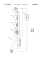
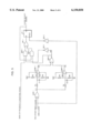
- FIG. 1 shows a block diagram indicating a conventional DPPLL structure.
- the DPPLL comprises a divider 11 for dividing a system clock with a predetermined dividing rate and feedbacking the system clock, a phase comparator 12 for calculating a phase difference by comparing phases of the system clock divided from the divider 11 with the reference clock and outputting the phase difference by use of the pulse width, a phase difference counter 13 for counting an output of the phase comparator 12 with the system clock, a microprocessor(digital filter) 14 for averaging the differential phases difference by receiving counted results from the counter 13, a D/A converter 15 for converting the average from the microprocessor 14 to a corresponding analog amplitude signal, and a voltage controlled crystal oscillator(hereinafter, referred to VCXO) 16 for oscillating a frequency clock in accordance with the analog amplitude signal.
- the phase comparator 12 consists of an invertor and an AND gate.
- the divider 11 divides the system clock oscillated from the VCXO 16 by a predetermined dividing rate and applies the system clock to the phase comparator 12.
- phase comparator 12 inverts the clock via the divider 11 in the inverter and applies to the AND gate, and the AND gate and-operates the inverted signal and the reference clock.
- the comparator 12 compares the phase of the system clock divided through the divider 11 with the phase of the reference clock, calculates the phase difference, modulates the phase difference by use of pulse width and outputs the pulse width.
- phase difference counter 13 counts the phase difference pulse applied from the phase comparator 12 by using an express system clock feedbacked from the VCXO 16, and applies the count value(N) to the microprocessor(digital filter) 14.
- the microprocessor 14 receives several count values as much as the phase difference applied from the counter 13, successively, averages the counter values and outputs the average values to the D/A converter 15. And the D/A converter 15 converts the average values from the microprocessor 14 to a corresponding analog amplitude value, and applies the analog value to the VCXO 16.
- the VCXO 16 oscillates a clock of frequency in accordance with the analog amplitude value applied from the converter 15, and later system clock repeats like above operation. Consequently, frequency becomes quicker or slower according to the reference clock, so it is capable of acquiring the system clock of which frequency is compensated gradually.
- the DPPLL may compensate a phase difference pulse amplitude only, in which the phase difference pulse amplitude corresponds to one cycle of the system clock(the digital count value is 1) or more than one cycle of the system clock(the digital count value is over 1).
- the DPPLL may compensate a phase difference pulse amplitude only, in which the phase difference pulse amplitude corresponds to one cycle of the system clock(the digital count value is 1) or more than one cycle of the system clock(the digital count value is over 1).
- the count value may be outputted from the counter 13 as over 1 when the phase difference pulse amplitude from the comparator 12 is over about 100 ns. In other words, it is difficult to sense when the phase difference is under 100 ns.
- SDH synchronous digital hierarchy
- the system clock phases of the pair of clock units may be have 180 degree difference, or 90 to 270.
- a first object of the present invention is to provide a phase compensation circuit of a DPPLL capable of hitless switching during switching the system clock, by exact matching frequency and phase of the DPPLL about phase difference which is less than minimum phase difference which may be detectable the way of digital(phase difference having less than one cycle of the system clock), in which the DPPLL is established in order to compensate by detecting the phase difference of the system clock and the reference clock by the digital way.
- a second object of the present invention is to provide a phase compensation circuit of a DPPLL capable of hitless switching, by distinguishing phase difference about the other party clock such that each clock unit commonly has the clock generated from the pair of clock units, alternatively and by switching the system clock in case that there is no difference after distinguishing, in the clock supplying system using the pair of clock units which have the phases that is asynchronized to the reference clock.
- One embodiment of the present invention to achieve the first object provides a digital processing phase-locked loop(DPPLL), comprising a first detecting path of detecting a differential phase value of a pulse outputted from phase comparating means, by use of a digital value, a second detecting path of detecting the differential phase value of the pulse by use of an analog value, control means for comparing the digital differential phase value with a system clock value and selecting and outputting the analog differential phase value in case that the digital differential phase value is smaller than a specific range of the system clock value, and voltage controlled oscillating means for outputting a phase compensated system clock by using the outputted signal.
- DPLL digital processing phase-locked loop
- the other embodiment of the present invention to achieve the second object provides a digital processing phase-locked loop(DPPLL), comprising a first detecting path of detecting a differential phase value of a pulse outputted from phase comparating means, by use of a digital value, a second detecting path of detecting the differential phase value of the pulse by use of an analog value, control means for comparing the digital differential phase value with a system clock value and selecting and outputting the analog differential phase value in case that the digital differential phase value is smaller than a specific range of the system clock value, voltage controlled oscillating means for outputting a phase compensated system clock by using the outputted signal, and phase switching means for switching a system clock in a corresponding area by detecting an area where the differential phase is smaller than a specific range of the system clock value, after comparing the phase of the clock with clock from the other unit.
- DPLL digital processing phase-locked loop
- FIG. 1 is a block diagram indicating a structure of a conventional DPPLL
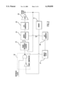
- FIG. 2 is a block diagram of a phase compensation circuit of a DPPLL according to a first embodiment of the present invention
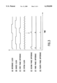
- FIG. 3 is an operational timing flowchart of each part of FIG. 2,
- FIG. 4 is a block diagram indicating a phase compensation circuit of a DPPLL for hitless switching according to a second embodiment of the present invention
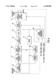
- FIG. 5 is in detail a circuit diagram of a phase difference comparator of FIG. 4, and
- FIG. 6 is an operational timing flowchart of each part of FIG. 5.
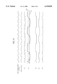
- FIG. 2 shows a block diagram of a phase compensation circuit of a DPPLL according to the first embodiment of the present invention. It is comprised of a divider 21, a phase comparator 22, a phase difference counter 23, a microprocessor 24, a D/A converter 25, a VCXO 26, an analog filter 27, and an A/D converter 28 for filtering a phase difference pulse according to amplitude, respectively after comparing phases of system clock and reference clock, averaging the phase difference, making an oscillating control voltage with the average, and outputting frequency and the phase compensated system clock.
- FIG. 3 shows an operational time diagram indicating a change of the phase difference referring to the FIG. 2.
- phase comparator 22 differential phase counter 23, D/A convertor 25, and the VCXO 26 are identified by the same structure of FIG. 1, and will not be described.
- the analog filter 27 changes the phase difference pulse width applied from the comparator 22 to an analog amplitude value, and applies the corresponding converted analog amplitude value to the A/D converter 28.
- the A/D converter 28 converts the analog amplitude value to a corresponding digital value and applies the digital value to the microprocessor 24.
- the microprocessor 24 selects one among the phase difference count values from the counter 22 or the digital values from the A/D convertor 28 according to an internal logic of the microprocessor 24 and averages the selected value, and then applies the corresponding average value to the D/A convertor 25.
- the microprocessor 24 selects the differential count value when the phase difference count value is over 1 in the counter 23 and the digital value from the A/D convertor 28 when the phase difference count value is 0 in the counter 23, and then filters the selected value. It is possible to do by designing as duplicating a filter structure coefficient during programming of the microprocessor.
- the divider 21 divides the system clock generated from the VCXO 26, by a predetermined dividing rate and applies to the phase comparator 22 in order to compare the phases of the reference clock and the system clock in the DPPLL operation.
- phase comparator 22 inverts the clock signal from the divider 21 through an inverter and applies the inverted clock signal to the AND gate and the AND gate and-operates the inverted system clock(shown in FIG. 3b) and the reference clock(shown in FIG. 3a) and outputs the phase difference pulse(shown in FIG. 3c) after comparing the two clock phases.
- the phase difference counter 23 counts the differential phase pulse by use of an express system clock(shown in FIG. 3d) oscillated from the VCXO 26 in order to sense the phase pulse difference width applied from the comparator 22, and outputs the count value.
- the phase difference counter 23 applies the count value having "n" bits according to the design structure of the clock system to the microprocessor(digital filter) 24 in the DPPLL.
- analog filter 27 changes the phase difference pulse width from the comparator 22 to an analog amplitude value, and converts the corresponding analog amplitude value to a digital value through the A/D converter 28 and applies the digital values to the microprocessor 24.
- the microprocessor 24 sets the internal logic in order to receive the digital count value of the counter 23 as an input when the phase difference count value is over 1. So, the count value having "n" bits from the counter 23 is filtering like a formula 1 below in the microprocessor 24.
- the "M” indicates number of times that the count value having the "n” bits from the differential counter 23 is applied
- “C(M)” is the count value having the "n” bits applied at the "M” th
- " ⁇ C(M)” indicates a sum of the count values having the "n” bits applied during the "M” times successively
- the "A” is an average of the count values having the "n” bits applied during the "M” times successively.
- the average value(A) calculated from the microprocessor 24 is outputted to the D/A converter 25, the D/A converter 25 converts the average value(A) to a corresponding analog amplitude value, and controls an oscillating voltage of the VCXO 26 by applying the corresponding converted analog amplitude value to the VCXO 26.
- the VCXO 26 oscillates and outputs the system clock of frequency in accordance with the analog amplitude value from the D/A converter 25.
- system clock outputted form the VCXO 26 is applied to the divider 21 and the divider 21 divide the system clock by a predetermined dividing rate for comparing the phase difference with the reference clock. And the above operation is repeated, successively.
- the phase difference counter 23 may not carry out counting the differential pulse amplitude any more.
- the microprocessor 24 is already designed for capable of switching about two inputs(digital count value and analog amplitude value) when the count value of the counter 23 is less then 1 (when the differential pulse width from the comparator is changed to less than one cycle of the system clock).
- the internal switching operation is accomplished in the microprocessor 24, and the second phase difference pulse inputted through the analog filter 27 and A/D converter 28, is applied to the microprocessor 24.
- the digital value applied from the A/D converter 28 is filtering like below formula 2 in the microprocessor 24.
- n' is number of times that the phase difference count value is less than 1
- C(M')' indicates a corresponding digital value in case that the phase difference count value is less than 1
- A' indicates a phase difference average value in case that the differential phase difference count value is less than 1.
- the D/A converter 25 converts the average value(A') to the analog amplitude value and applies the analog amplitude value to the VCXO 26.
- the VCXO 26 oscillates the system clock of the frequency in accordance with the analog amplitude value applied from the D/A converter 25, and outputs the system clock.
- phase difference width becomes 0 gradually like a third phase difference pulse(FIG. 3f) or a fourth phase difference pulse(FIG. 3g) when the above operation, in which the system clock oscillated from the VCXO 26 is applied to the divider 21 and divided, is successively repeated.
- the differential phase pulse width becomes larger and the digital count value of the phase difference counter 23 is over 1.
- the "C(M)" value may be an outputting value from the counter 23 or the A/D converter 28 during the "M" times.
- the "n” may be different according to a design structure and clock frequency according to the corresponding system, and the "M" and circle for controlling the VCXO 26, are acquired by theoretical calculation and repeated test with considering the system clock frequency, capacity of the microprocessor 24, the converting steps of the D/A converter 25, and etc.
- FIG. 4 is a block diagram indicating a phase compensation circuit of a DPPLL for hitless switching in duplicated clock suppling system by using the pair of clock units according to a second embodiment of the present invention. Referring to FIG. 4, one clock unit is only indicated.
- phase difference component 29, a clock selector 30, and a clock and reference signal supplier 31 in the DPPLL of FIG. 2 in order that a clock unit compares own clock with phase by commonly having the other party (lock and switching the system clock in an area where the phase differences is small.
- phase difference comparator 29 compares two clock phases by receiving the own clock and the other party clock as an input, detects an area where the phase difference is the shortest after comparing, and then generates an output(clock select signal).
- the (clock selector 30 selects the own clock or the other party clock according to the clock select signal and applies the own clock or the other party clock to the clock and reference signal supplier 31.
- the supplier 31 supplies the reference signal and the clock by outputting the own clock in case of main unit and supplies the reference signal and the clock by outputting the other party clock in case of reserved unit according to the clock applied from the clock selector 30.
- the phases of two clocks and reference signal are always same in a unit which receives the clock and reference signal. The reason is that the main unit and the reserved unit are operated using one's DPPLL but the outputting clock is the one of the main unit. In other words, source of the output clock of the pair of units is one.
- FIG. 5 shows in detail a circuit diagram of a phase difference comparator.
- a phase difference of own clock and other party clock are outputted as a pulse((1) wave of FIG. 6) through an exclusive OR gate.
- the pulse of the phase difference is converted to a corresponding direct current(DC) level((2) wave of FIG. 6) through a plurality of registers and capacitors.
- the DC level is compared with an upper reference value(a) by using a first voltage comparator(COMP 1) and with a lower reference value(b) by using a second voltage comparator(COMP2). In case that the DC level is higher than the upper reference value or lover than the lower reference value, logic high is outputted((3), (4) waves of FIG. 6) through the two voltage comparators.
- the registers and capacitors for converting the phase difference to the DC level should be adjusted according to a corresponding clock frequency.
- Two pulses outputted from the comparators(COMP1, 2) are through a NOR gate(NOR1) and an output of the NOR1((5) wave of FIG. 6) is inputted as a clock select signal of the clock selector 30 which comprises two AND gates(AND1, 2), an invertor(INV1), an OR gate(OR1) and a flipflop(FF1).
- the clock select signal to the clock selector 30 is outputted to the trailing edge of the own clock during logic high.
- the reason why the clock select signal is outputted to the trailing edge of the own clock, is, that a positive edge of an unwanted clock is outputted in case of not using the FF1 at the moment when the other party clock is logic low and own clock is logic high(it is assumed that the clock supply system use the positive edge).
- FIG. 6 is an operational timing flowchart of each part of the FIG. 5.
- a clock select signal outputted from the other embodiment of the present invention may be outputted in case that clock phases have a phase difference which does not affect a system.
- a clock from the clock selector 30 is outputted as own clock and inputted to the clock and reference signal supplier 31.
- the supplier 31 outputs own reference clock in case of main unit and the other party reference clock in case of reserved unit according to states of main or reserved unit. Consequently, the clock as well as the reference signal which are absolutely matched in the pair of units, are outputted.
- the present invention always matches the phases in case of matching the absolute phase shown in FIG. 2.
- the reference clock of the SDH N/W includes own jitter in the system because the reference clock is inputted to the system through several steps, oscillates in a hold-over mode by the reference clock missing and is in a free-running state by user's choice. Therefore, it may prevent sudden problems in the system by switching according to the phase difference after comparing the clocks of each other in any situation.
- the present invention by matching an absolute phase to the reference clock in case of receiving a proper reference clock, it is capable of switching without any effect to the system during switching between the pair of clock units. Additionally, if the reference clock has problems or the clock is cutting, output of the pair of clock units are not matching, successively. Therefore, it is capable of hitless switching by switching in case that the phase is synchronized.
Abstract
Description
A=ΣC(M)/M formula 1.
A'=ΣC(M')'/n' formula 2
Claims (11)
Applications Claiming Priority (2)
| Application Number | Priority Date | Filing Date | Title |
|---|---|---|---|
| KR2019970042821U KR200314154Y1 (en) | 1997-12-29 | 1997-12-29 | Apparatus For Compensing Frequency And Phase Simultaneously In DPPLL |
| KR97-42821U | 1997-12-29 |
Publications (1)
| Publication Number | Publication Date |
|---|---|
| US6150858A true US6150858A (en) | 2000-11-21 |
Family
ID=19519410
Family Applications (1)
| Application Number | Title | Priority Date | Filing Date |
|---|---|---|---|
| US09/218,772 Expired - Fee Related US6150858A (en) | 1997-12-29 | 1998-12-22 | Phase compensation circuit of digital processing PLL |
Country Status (3)
| Country | Link |
|---|---|
| US (1) | US6150858A (en) |
| KR (1) | KR200314154Y1 (en) |
| CN (1) | CN1156085C (en) |
Cited By (8)
| Publication number | Priority date | Publication date | Assignee | Title |
|---|---|---|---|---|
| US20030090305A1 (en) * | 2001-11-02 | 2003-05-15 | Yoshihiro Kobayashi | Clock shaping circuit and electronic equipment |
| US6731158B1 (en) * | 2002-06-13 | 2004-05-04 | University Of New Mexico | Self regulating body bias generator |
| WO2004086686A1 (en) * | 2003-03-25 | 2004-10-07 | Utstarcom Korea Limited | Apparatus of network synchronization and switching for use in atm exchanger |
| US20040221188A1 (en) * | 2000-02-18 | 2004-11-04 | Rambus Inc. | Apparatus and method for providing a clock signal for testing |
| US20060022728A1 (en) * | 2004-07-29 | 2006-02-02 | Intel Corporation | Frequency-controlled DLL bias |
| US20080042755A1 (en) * | 2006-08-07 | 2008-02-21 | Gennady Feygin | Method and apparatus to provide digitally controlled crystal oscillators |
| US20080042708A1 (en) * | 2006-06-19 | 2008-02-21 | Hiroki Kimura | PLL oscillation circuit |
| CN111934842A (en) * | 2020-07-08 | 2020-11-13 | 中北大学 | Electrical phase-stable clock distribution system and method |
Families Citing this family (1)
| Publication number | Priority date | Publication date | Assignee | Title |
|---|---|---|---|---|
| KR100809801B1 (en) * | 2001-12-24 | 2008-03-04 | 엘지노텔 주식회사 | Method for holdover handling in phase-locked loop |
Citations (5)
| Publication number | Priority date | Publication date | Assignee | Title |
|---|---|---|---|---|
| US5673004A (en) * | 1994-09-15 | 1997-09-30 | Lg Information & Communications, Ltd | Method and circuit for controlling digital processing phase-locked loop for network synchronization |
| US5696468A (en) * | 1996-02-29 | 1997-12-09 | Qualcomm Incorporated | Method and apparatus for autocalibrating the center frequency of a voltage controlled oscillator of a phase locked loop |
| US5917873A (en) * | 1996-10-08 | 1999-06-29 | Sony Corporation | Receiving apparatus, receiving method, and digital PLL circuit |
| US5920214A (en) * | 1996-03-30 | 1999-07-06 | Samsung Electronics, Co., Ltd. | Method and apparatus for generating an eight-to-fourteen modulation data restoring clock signal |
| US5986485A (en) * | 1996-08-26 | 1999-11-16 | Nec Corporation | Auto-lock circuit guaranteeing low jitter in phase-locked loop frequency synthesizers irrespective of process variations |
-
1997
- 1997-12-29 KR KR2019970042821U patent/KR200314154Y1/en not_active IP Right Cessation
-
1998
- 1998-12-22 US US09/218,772 patent/US6150858A/en not_active Expired - Fee Related
- 1998-12-29 CN CNB981266088A patent/CN1156085C/en not_active Expired - Fee Related
Patent Citations (5)
| Publication number | Priority date | Publication date | Assignee | Title |
|---|---|---|---|---|
| US5673004A (en) * | 1994-09-15 | 1997-09-30 | Lg Information & Communications, Ltd | Method and circuit for controlling digital processing phase-locked loop for network synchronization |
| US5696468A (en) * | 1996-02-29 | 1997-12-09 | Qualcomm Incorporated | Method and apparatus for autocalibrating the center frequency of a voltage controlled oscillator of a phase locked loop |
| US5920214A (en) * | 1996-03-30 | 1999-07-06 | Samsung Electronics, Co., Ltd. | Method and apparatus for generating an eight-to-fourteen modulation data restoring clock signal |
| US5986485A (en) * | 1996-08-26 | 1999-11-16 | Nec Corporation | Auto-lock circuit guaranteeing low jitter in phase-locked loop frequency synthesizers irrespective of process variations |
| US5917873A (en) * | 1996-10-08 | 1999-06-29 | Sony Corporation | Receiving apparatus, receiving method, and digital PLL circuit |
Cited By (12)
| Publication number | Priority date | Publication date | Assignee | Title |
|---|---|---|---|---|
| US20040221188A1 (en) * | 2000-02-18 | 2004-11-04 | Rambus Inc. | Apparatus and method for providing a clock signal for testing |
| US20030090305A1 (en) * | 2001-11-02 | 2003-05-15 | Yoshihiro Kobayashi | Clock shaping circuit and electronic equipment |
| US6703877B2 (en) * | 2001-11-02 | 2004-03-09 | Seiko Epson Corporation | Clock shaping circuit and electronic equipment |
| US6731158B1 (en) * | 2002-06-13 | 2004-05-04 | University Of New Mexico | Self regulating body bias generator |
| WO2004086686A1 (en) * | 2003-03-25 | 2004-10-07 | Utstarcom Korea Limited | Apparatus of network synchronization and switching for use in atm exchanger |
| US20060022728A1 (en) * | 2004-07-29 | 2006-02-02 | Intel Corporation | Frequency-controlled DLL bias |
| US7145373B2 (en) * | 2004-07-29 | 2006-12-05 | Intel Corporation | Frequency-controlled DLL bias |
| US20080042708A1 (en) * | 2006-06-19 | 2008-02-21 | Hiroki Kimura | PLL oscillation circuit |
| US7656208B2 (en) * | 2006-06-19 | 2010-02-02 | Nihon Dempa Kogyo., Ltd. | PLL oscillation circuit |
| US20080042755A1 (en) * | 2006-08-07 | 2008-02-21 | Gennady Feygin | Method and apparatus to provide digitally controlled crystal oscillators |
| US7808327B2 (en) * | 2006-08-07 | 2010-10-05 | Texas Instruments Incorporated | Method and apparatus to provide digitally controlled crystal oscillators |
| CN111934842A (en) * | 2020-07-08 | 2020-11-13 | 中北大学 | Electrical phase-stable clock distribution system and method |
Also Published As
| Publication number | Publication date |
|---|---|
| CN1156085C (en) | 2004-06-30 |
| KR200314154Y1 (en) | 2003-08-14 |
| KR19990030150U (en) | 1999-07-26 |
| CN1230052A (en) | 1999-09-29 |
Similar Documents
| Publication | Publication Date | Title |
|---|---|---|
| US6480047B2 (en) | Reduced jitter phase lock loop using a technique multi-stage digital delay line | |
| RU2127485C1 (en) | Phase-locking method and circuit for phase- locked system | |
| JP3066690B2 (en) | Phase-locked oscillation circuit | |
| US5373254A (en) | Method and apparatus for controlling phase of a system clock signal for switching the system clock signal | |
| US5459435A (en) | Frequency synchronous circuit for obtaining original clock signal by removing noise components | |
| US7479814B1 (en) | Circuit for digital frequency synthesis in an integrated circuit | |
| US6049238A (en) | Clock generator and clock generating method capable of varying clock frequency without increasing the number of delay elements | |
| JP2000124802A (en) | Pll circuit | |
| JPH06102964A (en) | Information processing system | |
| US6150858A (en) | Phase compensation circuit of digital processing PLL | |
| JPH08265140A (en) | Method and device for determining feedback frequency demultiplying ratio in phase-locked loop | |
| JP4015254B2 (en) | Lock detection circuit and PLL frequency synthesizer | |
| EP0670635B1 (en) | Phase-locked loop oscillator, and moving-average circuit, and division-ratio equalization circuit suitable for use in the same | |
| US6166606A (en) | Phase and frequency locked clock generator | |
| US6411143B1 (en) | Lock detector for a dual phase locked loop system | |
| JP2996205B2 (en) | PDH low-speed signal switching DPLL | |
| JP3281820B2 (en) | PLL frequency synthesizer | |
| JPWO2004047301A1 (en) | Frequency synthesizer | |
| US5867545A (en) | Phase-locked loop circuit | |
| JPS58168333A (en) | Phase comparing system of phase locking loop circuit | |
| JPH07273648A (en) | Pll circuit | |
| JPH08331085A (en) | Digital phase synchronization circuit and data reception circuit using it | |
| KR100560434B1 (en) | Apparatus for providing system clock synchronized to network universally | |
| JPH11298460A (en) | Clock changeover circuit | |
| JP2908293B2 (en) | Digital phase locked loop circuit |
Legal Events
| Date | Code | Title | Description |
|---|---|---|---|
| AS | Assignment |
Owner name: LG INFORMATION & COMMUNICATIONS, LTD., KOREA, REPU Free format text: ASSIGNMENT OF ASSIGNORS INTEREST;ASSIGNOR:SUNG, WON SIK;REEL/FRAME:009673/0907 Effective date: 19981214 |
|
| FEPP | Fee payment procedure |
Free format text: PAYOR NUMBER ASSIGNED (ORIGINAL EVENT CODE: ASPN); ENTITY STATUS OF PATENT OWNER: LARGE ENTITY |
|
| FPAY | Fee payment |
Year of fee payment: 4 |
|
| AS | Assignment |
Owner name: LG ELECTRONICS INC., KOREA, REPUBLIC OF Free format text: MERGER;ASSIGNOR:LG INFORMATION & COMMUNICATIONS, LTD.;REEL/FRAME:017154/0033 Effective date: 20000904 |
|
| AS | Assignment |
Owner name: LG NORTEL CO., LTD., KOREA, REPUBLIC OF Free format text: ASSIGNMENT OF ASSIGNORS INTEREST;ASSIGNOR:LG ELECTRONICS INC.;REEL/FRAME:018296/0720 Effective date: 20060710 |
|
| FPAY | Fee payment |
Year of fee payment: 8 |
|
| AS | Assignment |
Owner name: LG-ERICSSON CO., LTD., KOREA, REPUBLIC OF Free format text: CHANGE OF NAME;ASSIGNOR:LG-NORTEL CO., LTD.;REEL/FRAME:025948/0842 Effective date: 20100630 |
|
| REMI | Maintenance fee reminder mailed | ||
| LAPS | Lapse for failure to pay maintenance fees | ||
| STCH | Information on status: patent discontinuation |
Free format text: PATENT EXPIRED DUE TO NONPAYMENT OF MAINTENANCE FEES UNDER 37 CFR 1.362 |
|
| FP | Lapsed due to failure to pay maintenance fee |
Effective date: 20121121 |