US7625472B2 - Plasma-assisted sputter deposition system - Google Patents

Plasma-assisted sputter deposition system Download PDF

Info

Publication number
US7625472B2
US7625472B2 US10/905,574 US90557405A US7625472B2 US 7625472 B2 US7625472 B2 US 7625472B2 US 90557405 A US90557405 A US 90557405A US 7625472 B2 US7625472 B2 US 7625472B2
Authority
US
United States
Prior art keywords
plasma
electrode
deposition system
sputter deposition
spinning plate
Prior art date
Legal status (The legal status is an assumption and is not a legal conclusion. Google has not performed a legal analysis and makes no representation as to the accuracy of the status listed.)
Expired - Fee Related, expires
Application number
US10/905,574
Other versions
US20050150457A1 (en
Inventor
Sunil Wickramanayaka
Current Assignee (The listed assignees may be inaccurate. Google has not performed a legal analysis and makes no representation or warranty as to the accuracy of the list.)
Canon Anelva Corp
Original Assignee
Canon Anelva Corp
Priority date (The priority date is an assumption and is not a legal conclusion. Google has not performed a legal analysis and makes no representation as to the accuracy of the date listed.)
Filing date
Publication date
Application filed by Canon Anelva Corp filed Critical Canon Anelva Corp
Assigned to ANELVA CORPORATION reassignment ANELVA CORPORATION ASSIGNMENT OF ASSIGNORS INTEREST (SEE DOCUMENT FOR DETAILS). Assignors: WICKRAMANAYAKA, SUNIL
Publication of US20050150457A1 publication Critical patent/US20050150457A1/en
Assigned to CANON ANELVA CORPORATION reassignment CANON ANELVA CORPORATION CHANGE OF NAME (SEE DOCUMENT FOR DETAILS). Assignors: ANELVA CORPORATION
Application granted granted Critical
Publication of US7625472B2 publication Critical patent/US7625472B2/en
Expired - Fee Related legal-status Critical Current
Adjusted expiration legal-status Critical

Links

Images

Classifications

    • CCHEMISTRY; METALLURGY
    • C23COATING METALLIC MATERIAL; COATING MATERIAL WITH METALLIC MATERIAL; CHEMICAL SURFACE TREATMENT; DIFFUSION TREATMENT OF METALLIC MATERIAL; COATING BY VACUUM EVAPORATION, BY SPUTTERING, BY ION IMPLANTATION OR BY CHEMICAL VAPOUR DEPOSITION, IN GENERAL; INHIBITING CORROSION OF METALLIC MATERIAL OR INCRUSTATION IN GENERAL
    • C23CCOATING METALLIC MATERIAL; COATING MATERIAL WITH METALLIC MATERIAL; SURFACE TREATMENT OF METALLIC MATERIAL BY DIFFUSION INTO THE SURFACE, BY CHEMICAL CONVERSION OR SUBSTITUTION; COATING BY VACUUM EVAPORATION, BY SPUTTERING, BY ION IMPLANTATION OR BY CHEMICAL VAPOUR DEPOSITION, IN GENERAL
    • C23C14/00Coating by vacuum evaporation, by sputtering or by ion implantation of the coating forming material
    • C23C14/22Coating by vacuum evaporation, by sputtering or by ion implantation of the coating forming material characterised by the process of coating
    • C23C14/34Sputtering
    • C23C14/35Sputtering by application of a magnetic field, e.g. magnetron sputtering
    • HELECTRICITY
    • H01ELECTRIC ELEMENTS
    • H01JELECTRIC DISCHARGE TUBES OR DISCHARGE LAMPS
    • H01J37/00Discharge tubes with provision for introducing objects or material to be exposed to the discharge, e.g. for the purpose of examination or processing thereof
    • H01J37/32Gas-filled discharge tubes
    • H01J37/34Gas-filled discharge tubes operating with cathodic sputtering
    • H01J37/3411Constructional aspects of the reactor
    • H01J37/345Magnet arrangements in particular for cathodic sputtering apparatus
    • H01J37/3455Movable magnets
    • HELECTRICITY
    • H01ELECTRIC ELEMENTS
    • H01JELECTRIC DISCHARGE TUBES OR DISCHARGE LAMPS
    • H01J37/00Discharge tubes with provision for introducing objects or material to be exposed to the discharge, e.g. for the purpose of examination or processing thereof
    • H01J37/32Gas-filled discharge tubes
    • H01J37/34Gas-filled discharge tubes operating with cathodic sputtering
    • H01J37/3402Gas-filled discharge tubes operating with cathodic sputtering using supplementary magnetic fields
    • H01J37/3405Magnetron sputtering
    • GPHYSICS
    • G11INFORMATION STORAGE
    • G11BINFORMATION STORAGE BASED ON RELATIVE MOVEMENT BETWEEN RECORD CARRIER AND TRANSDUCER
    • G11B5/00Recording by magnetisation or demagnetisation of a record carrier; Reproducing by magnetic means; Record carriers therefor
    • G11B5/84Processes or apparatus specially adapted for manufacturing record carriers
    • G11B5/851Coating a support with a magnetic layer by sputtering

Definitions

  • the present invention relates to a plasma-assisted sputter deposition system, and more particularly, to a plasma-assisted sputter deposition system for depositing thin films on a wafer, in which a wafer holder is at rest during the film deposition, with a great uniformity and a great accuracy of film thickness controllability.
  • Magnetron DC or RF sputtering systems are in wide application to deposit thin films on substrates used in semiconductor industry.
  • a DC sputtering system with an angled electrode with respect to wafer surface has been invented and in use (JP-A-2002-167661 and JP-A-2002-296413).
  • this system has some problems in controlling the substrate temperature, re-sputtering of deposited film and particle reduction. These problems are explained in detail with reference to FIG. 5 .
  • FIG. 5 shows a cross sectional view of a DC sputtering system with an angled electrode.
  • the reactor 100 is comprised of an electrode 101 , a wafer holder 102 , gas inlets 103 and a gas outlet 104 .
  • the electrode 101 is made of a metal, for example, Al, Ti, Ta etc. that needs to be sputtered and deposited on a wafer 112 .
  • the electrode 101 is electrically isolated from the reactor 100 using a dielectric material 105 .
  • a plurality of magnets 106 with some specific arrangement has been placed.
  • magnets 106 arranged to the electrode 101 are rotated around an off-axis or the central axis of the electrode 101 .
  • a round arrow 121 shows the state of rotation movement around the central axis.
  • the electrode 101 is connected to a DC power source 107 .
  • the wafer holder 102 is comprised of a metal electrode 108 , dielectric material 109 , side-walls 110 and a shaft 111 .
  • the shaft 111 is connected to an electrical motor in order to rotate the wafer holder 102 on its central axis as shown by a round arrow 122 .
  • the electric motor is not shown in the figure.
  • DC plasma is generated within the reactor 100 by applying a DC current to the electrode 101 while maintaining a low pressure inside the reactor 100 . Owing to the higher negative voltage of the electrode 101 , ions in the plasma are accelerated to the electrode 101 and sputtered. These sputtered atoms then travel through the plasma and deposit on the wafer 112 and other surfaces, which are exposed to plasma.
  • the sputtered-atom flux coming from the angled electrode 101 is not uniform on the wafer surface.
  • the wafer holder 102 is rotated around its central axis. This results in a uniform film. All the problems in the above-explained PVD system come due to the wafer holder 102 being rotated.
  • the first problem is that wafer temperature during the film deposition cannot be controlled. This is because incorporation of a liquid-base cooling mechanism for the metal electrode 108 is difficult. Incorporation of a heating mechanism for the metal electrode 108 is also difficult. These difficulties are mechanical difficulties and arise due to the rotation of wafer holder 102 . Deposition of films at a controlled temperature is of importance in obtaining films with desired physical and electrical properties. For example, deposition of Cu films as a seed layer for electroplating process has to be carried out at a temperature below zero for better surface smoothness.
  • the second problem is that fabrication of electrostatic chuck (ESC) on the metal electrode 108 to clamp the wafer by using electrostatic force is difficult due to the complexity in designing electrical connections. Wafer clamping by using the ESC is important when control on wafer temperature is needed during the film deposition process.
  • ESC electrostatic chuck
  • the third problem is that the supply of a rf current to the metal electrode 108 is also not easy due to the difficulty in making electrical connection to the rotating wafer holder 102 .
  • Application of the rf power to the metal electrode 108 is needed if the deposition has to be carried out with the bombardment of soft-ions or if the deposited film is needed to be re-sputtered.
  • the forth problem is the generation of particles within the reactor due to continuity of rotation of the wafer holder 102 .
  • the rotation of the wafer holder 102 causes vibration of its outer parts and peripheral parts. This eases delaminating of deposited film from the vibrating surfaces, which finally causes particle contamination on the wafer surface.
  • the wafer holder is at rest when processing the wafers, by changing or improving the structure of the electrode and related sections.
  • An object of the present invention is to provide a plasma-assisted sputter deposition system capable of solving the above-mentioned problems and maintaining good and required qualities such as film uniformity and thickness controllability by employing a doughnut-shape electrode with an angled surface, a magnet configuration with rotation and revolution (planetary motion), and a temperature-controllable wafer holder which is at rest during the film deposition.
  • a plasma-assisted sputter deposition system in accordance with an embodiment of the present invention is configured as follows in order to attain the above-mentioned object.
  • a plasma-assisted sputter deposition system is comprised of a reactor into which a process gas is introduced to be used for producing plasma; a doughnut-shaped electrode made of a material for sputtering by the plasma, wherein a lower surface of the doughnut-shaped electrode is angled or parallel to a surface of a wafer; a spinning plate that spins on its central axis while moving over a circle above the doughnut-shaped electrode, wherein the spinning plate contains magnet arrangement attached to its lower surface and is parallel to the surface of the doughnut-shaped electrode; an electrical power sources connected to the doughnut-shaped electrode, and a wafer holder for placing the wafer for film deposition, which is at rest during the film deposition.
  • the magnet arrangement on the lower surface of the spinning plate is symmetric around its spinning axis.
  • the magnet arrangement on the lower surface of spinning plate is asymmetric around its spinning axis.
  • a plasma-assisted sputter deposition system is comprised of a reactor into which a process gas is introduced to be used for producing plasma; a doughnut-shaped electrode made of a material for sputtering by the plasma, wherein a lower surface of the doughnut-shaped electrode is angled or parallel to a surface of a wafer; two or more circular magnets with different diameters and placed above the doughnut-shaped electrode to have alternate polarities facing the electrode to generate one or more close-loop magnetic flux lines below the doughnut-shaped electrode; an electrical power sources connected to the doughnut-shaped electrode, and a wafer holder for placing the wafer for film deposition, which is at rest during the film deposition.
  • the plasma-assisted sputter deposition system in accordance with an embodiment of the present invention can maintain good and required qualities such as film uniformity and thickness controllability by employing a doughnut-shape electrode with an angled surface, a magnet configuration with a rotation and revolution, and a temperature-controllable wafer holder being at rest during the film deposition.
  • FIG. 1 is a longitudinal cross sectional diagram of the system of a first embodiment of the present invention
  • FIG. 2 is a perspective view of a doughnut-shaped electrode
  • FIG. 3 is a schematic plan view of the doughnut-shaped electrode together with the movements of the spinning plate to the doughnut-shaped electrode;
  • FIG. 4 is a longitudinal cross sectional diagram of the system of a second embodiment of the present invention.
  • FIG. 5 is a longitudinal cross sectional diagram of the conventional system.
  • FIG. 1 shows a longitudinal cross sectional diagram of the first embodiment of the plasma-assisted sputter deposition system of the present invention.
  • the reactor 1 is provided with an electrode 2 arranged on its ceiling wall 1 A and a wafer holder 5 arranged on its bottom plate 17 .
  • An upper-side support wall 1 B supports the ceiling wall 1 A.
  • the ceiling wall 1 A has a ring-shaped angled peripheral section.
  • the electrode 2 is placed in the ring-shaped angled peripheral section of the ceiling wall 1 A.
  • the electrode 2 is made of a metal such as Al, Ti, Ta etc. that is sputtered and deposited on a wafer 9 placed on the wafer holder 5 .
  • the electrode 2 is electrically isolated from the reactor 1 using a dielectric material 8 .
  • the electrode 2 is connected to a DC electric power source 10 .
  • the electrode 2 is of a doughnut-shape or circular ring-shape, and there are gas inlets 6 at the bottom plate 17 and a gas outlet 7 at the lower section of the side wall 20 near the bottom plate 17 .
  • a spinning plate or disk 3 In the space at back of the electrode 2 there is a spinning plate or disk 3 to which a magnet arrangement 4 is attached.
  • the electrode 2 is made of a material that is sputtered and deposited on the wafer 9 .
  • the shape of the electrode 2 is circular with a hole in the center as shown in FIG. 2 .
  • the inner and outer diameters of the electrode 2 are not critical and decided by considering the wafer diameter and height from the wafer to the electrode 2 .
  • the centers of inner and outer diameters of the electrode 2 and the center of wafer 9 lie on the same straight line.
  • the surfaces of electrode 2 are angled such that extension of these surfaces makes a conical-shape structure.
  • the angle between the electrode surface and a horizontal line, which is denoted by “ ⁇ ” in FIG. 1 is not critical and generally smaller than 45°.
  • is equal to 0, that is, that the electrode surface is parallel to the wafer surface.
  • the thickness of the electrode 2 denoted by “t” in FIG. 2 is also not critical and can lie in the range of 2 mm to 20 mm. A thinner electrode 2 is preferable as it yields a higher magnetic flux on its lower surface.
  • the electrode 2 is covered by an insulating material 8 in order to electrically isolate from the rest of the parts of the reactor 1 and is given a DC or rf electrical power. As one example, a DC power source 10 is shown in FIG. 1 .
  • the magnet arrangement 4 comprised of a plurality of magnets is fixed to the spinning plate 3 .
  • the spinning plate 3 is usually made of a metal.
  • the diameter of the spinning plate 3 is usually taken slightly shorter than the width of the electrode 2 denoted by “d” in FIG. 2 .
  • the spinning plate 3 constantly spins on its central axis 16 .
  • the spinning plate 3 with the magnet arrangement 4 moves on a circular path above the electrode 2 similar to planetary motion.
  • the spinning plate 3 is parallel to the surface of the doughnut-shaped electrode 2 .
  • a mechanism for making the spin motion and the planetary motion is comprised of a motor 33 connected to the central axis 16 , a ring-shape guide member with a gear mechanism fixed to the side-wall 20 of the upper-side support wall 1 B, and an connecting member for connecting the motor 33 and the ring-shaped guide member 34 .
  • the motor 33 operates, the central axis 35 is rotated and the unit including the motor 33 and the spinning plate 3 is moved along the ring-shaped guide member 34 through the gear mechanism.
  • the magnet arrangement 4 below the spinning plate 3 is not critical and may be any symmetric or asymmetric magnet arrangement.
  • the wafer holder 5 is fixed to the bottom plate 17 . It is comprised of a metal electrode 11 , an electric static chuck (ESC) 12 or a thin dielectric layer 12 , and an insulator 13 .
  • the metal electrode 11 is supplied with a temperature-controlled liquid via a liquid inlet 14 and an outlet 15 .
  • the temperature-controlled liquid is used to maintain a constant temperate usually in the range of 100° C. to ⁇ 100° C. on the metal electrode 11 . If a higher temperature, generally over 100° C. is needed, one can fix an electrical heating system within the metal electrode 11 .
  • the wafer holder 5 is fixed on the bottom plate 17 of the reactor 1 . This eases making electrical wiring and cooling/heating mechanisms. However, one can make the wafer holder 5 movable in the vertical direction with the all facilities mentioned-above.
  • the important feature of the wafer holder 5 compared to that explained in prior art, is that the wafer and the wafer holder are at rest during the film deposition. That is there are no any rotating parts of the wafer holder 5 .
  • the operation of the above-mentioned structure is explained.
  • the wafer 9 which is introduced into the reactor 1 through a wafer in/out door 18 is placed on the fixed wafer holder 5 .
  • the wafer 9 in the wafer holder 5 is electrostatically clamped on the ESC.
  • the ESC is maintained to be a constant temperature with the assist of coolant or a heater.
  • a gas is fed into the reactor 1 and the reactor is maintained a desired pressure.
  • the pressure inside the reactor 1 is not critical and can be vary in the range of 0.1 mTorr to 100 mTorr.
  • a DC electrical power is applied to the electrode 2 from the DC power source 10 to initiate and maintain plasma.
  • the electric power of the DC current applied to the electrode 2 is not important and is decided by the required deposition rate and other parameters.
  • a lower deposition rate for example 100 W
  • a lower power for example 100 W
  • the deposition has to be done at a lower rate, for example 10 nm/min.
  • a lower DC power for example 50 W
  • the plasma is concentrated below the spinning plate 3 since plasma is confined by the magnetic field.
  • This dense plasma moves on a circular path below the electrode 2 with the movement of the spinning plate 3 with magnet arrangement 4 .
  • the sputtering is mainly occurred at the place where the dense plasma is and the sputtered atoms reach the wafer surface with angles. Therefore, the film deposition process is almost similar to that explain in the prior art section resulting in a film with a very good film uniformity.
  • the metal electrode 11 in the wafer holder 5 may or may not be given an rf current. Even if a rf power is applied the power of the rf current from a rf power source 36 is usually kept a lower value so that there is no excessive sputtering of the deposited film.
  • the sputtering system of the first embodiment yields extremely uniform films with the controllability of film thickness with a great accuracy while the wafer temperature can be maintained at any desired value. Further, deposition can be performed with the soft-ion bombardment or with re-sputtering processes.
  • the wafer holder 5 is at rest and the plasma produced at a region under the electrode 2 , which corresponds to the magnet arrangement 4 of the spin plate 3 , is rotated together with the planetary movement (revolution) of the spin plate 3 . Therefore, even if the wafer holder 5 is not rotated, the uniform thin film is deposited onto the wafer 9 on the wafer holder 5 .
  • FIG. 4 It is a slight modification of the first embodiment.
  • the only modification in this system, compared to the first embodiment, is to use new structure of magnet arrangement corresponding to the magnet arrangement 4 without the above spinning plate 3 .
  • two or more circular magnets 19 a and 19 b are placed on the outside surface of the electrode 2 , which have alternate polarities facing the electrode surface. They are not moved.
  • a configuration with the two circular magnets 19 a and 19 b is shown in FIG. 4 , for example.
  • These two magnets 19 a and 19 b are permanently fixed on the electrode or placed with a small separation, for example 1 mm, with the electrode and slightly moved parallel to electrode surface.
  • There are magnetic flux lines 37 between the two circular magnets 19 a and 19 b The magnetic flux lines 37 penetrate the electrode 2 into the inside of reactor 1 .
  • the slight movement of the circular magnets 19 a and 19 b results in an improvement of electrode utilization efficiency.
  • the present invention is used for plasma-assisted magnetron sputtering without rotating the wafer holder, and useful for depositing films on the wafer with film uniformity and thickness controllability, and a temperature-controllable in the wafer holder.

Abstract

A plasma-assisted sputter deposition system includes a reactor 1 into which a process gas is introduced; a doughnut-shaped electrode to be sputtered by plasma, in which a lower surface thereof is angled to a surface of a wafer; a spinning plate that spin on its central axis while moving over a circle above the doughnut-shaped electrode, in which the spinning plate contains magnet arrangement; an electrical power sources connected to the doughnut-shaped electrode, and a wafer holder for placing a wafer for film deposition, which is at rest during the film deposition.

Description

BACKGROUND OF THE INVENTION
1. Field of the Invention
The present invention relates to a plasma-assisted sputter deposition system, and more particularly, to a plasma-assisted sputter deposition system for depositing thin films on a wafer, in which a wafer holder is at rest during the film deposition, with a great uniformity and a great accuracy of film thickness controllability.
2. Description of the Related Art
Magnetron DC or RF sputtering systems are in wide application to deposit thin films on substrates used in semiconductor industry. One of the major requirements in depositing films on substrates, for examples, on Si wafers, is the film uniformity. In order to deposit films with a greater uniformity, a DC sputtering system with an angled electrode with respect to wafer surface has been invented and in use (JP-A-2002-167661 and JP-A-2002-296413). However, this system has some problems in controlling the substrate temperature, re-sputtering of deposited film and particle reduction. These problems are explained in detail with reference to FIG. 5.
FIG. 5 shows a cross sectional view of a DC sputtering system with an angled electrode. The reactor 100 is comprised of an electrode 101, a wafer holder 102, gas inlets 103 and a gas outlet 104. The electrode 101 is made of a metal, for example, Al, Ti, Ta etc. that needs to be sputtered and deposited on a wafer 112. The electrode 101 is electrically isolated from the reactor 100 using a dielectric material 105. Generally, on the upper surface of electrode 101 a plurality of magnets 106 with some specific arrangement has been placed. Further, magnets 106 arranged to the electrode 101 are rotated around an off-axis or the central axis of the electrode 101. A round arrow 121 shows the state of rotation movement around the central axis. The electrode 101 is connected to a DC power source 107.
Usually, the wafer holder 102 is comprised of a metal electrode 108, dielectric material 109, side-walls 110 and a shaft 111. The shaft 111 is connected to an electrical motor in order to rotate the wafer holder 102 on its central axis as shown by a round arrow 122. The electric motor is not shown in the figure.
DC plasma is generated within the reactor 100 by applying a DC current to the electrode 101 while maintaining a low pressure inside the reactor 100. Owing to the higher negative voltage of the electrode 101, ions in the plasma are accelerated to the electrode 101 and sputtered. These sputtered atoms then travel through the plasma and deposit on the wafer 112 and other surfaces, which are exposed to plasma.
The sputtered-atom flux coming from the angled electrode 101 is not uniform on the wafer surface. In order to get a uniform film on the wafer surface, the wafer holder 102 is rotated around its central axis. This results in a uniform film. All the problems in the above-explained PVD system come due to the wafer holder 102 being rotated.
The first problem is that wafer temperature during the film deposition cannot be controlled. This is because incorporation of a liquid-base cooling mechanism for the metal electrode 108 is difficult. Incorporation of a heating mechanism for the metal electrode 108 is also difficult. These difficulties are mechanical difficulties and arise due to the rotation of wafer holder 102. Deposition of films at a controlled temperature is of importance in obtaining films with desired physical and electrical properties. For example, deposition of Cu films as a seed layer for electroplating process has to be carried out at a temperature below zero for better surface smoothness.
The second problem is that fabrication of electrostatic chuck (ESC) on the metal electrode 108 to clamp the wafer by using electrostatic force is difficult due to the complexity in designing electrical connections. Wafer clamping by using the ESC is important when control on wafer temperature is needed during the film deposition process.
The third problem is that the supply of a rf current to the metal electrode 108 is also not easy due to the difficulty in making electrical connection to the rotating wafer holder 102. Application of the rf power to the metal electrode 108 is needed if the deposition has to be carried out with the bombardment of soft-ions or if the deposited film is needed to be re-sputtered.
The forth problem is the generation of particles within the reactor due to continuity of rotation of the wafer holder 102. The rotation of the wafer holder 102 causes vibration of its outer parts and peripheral parts. This eases delaminating of deposited film from the vibrating surfaces, which finally causes particle contamination on the wafer surface.
In addition, as the related arts concerning cathode or target of doughnut-shaped, documents such as JP-A-7-126847 and JP-A-5-189762 may be cited.
OBJECTS AND SUMMARY
At present, it is desired to solve the above-mentioned four problems. In the magnetron DC or RF sputtering systems proposed by the present invention, the wafer holder is at rest when processing the wafers, by changing or improving the structure of the electrode and related sections.
An object of the present invention is to provide a plasma-assisted sputter deposition system capable of solving the above-mentioned problems and maintaining good and required qualities such as film uniformity and thickness controllability by employing a doughnut-shape electrode with an angled surface, a magnet configuration with rotation and revolution (planetary motion), and a temperature-controllable wafer holder which is at rest during the film deposition.
A plasma-assisted sputter deposition system in accordance with an embodiment of the present invention is configured as follows in order to attain the above-mentioned object.
A plasma-assisted sputter deposition system is comprised of a reactor into which a process gas is introduced to be used for producing plasma; a doughnut-shaped electrode made of a material for sputtering by the plasma, wherein a lower surface of the doughnut-shaped electrode is angled or parallel to a surface of a wafer; a spinning plate that spins on its central axis while moving over a circle above the doughnut-shaped electrode, wherein the spinning plate contains magnet arrangement attached to its lower surface and is parallel to the surface of the doughnut-shaped electrode; an electrical power sources connected to the doughnut-shaped electrode, and a wafer holder for placing the wafer for film deposition, which is at rest during the film deposition.
In the above plasma-assisted sputter deposition system, preferably, the magnet arrangement on the lower surface of the spinning plate is symmetric around its spinning axis.
In the plasma-assisted sputter deposition system, preferably, the magnet arrangement on the lower surface of spinning plate is asymmetric around its spinning axis.
A plasma-assisted sputter deposition system is comprised of a reactor into which a process gas is introduced to be used for producing plasma; a doughnut-shaped electrode made of a material for sputtering by the plasma, wherein a lower surface of the doughnut-shaped electrode is angled or parallel to a surface of a wafer; two or more circular magnets with different diameters and placed above the doughnut-shaped electrode to have alternate polarities facing the electrode to generate one or more close-loop magnetic flux lines below the doughnut-shaped electrode; an electrical power sources connected to the doughnut-shaped electrode, and a wafer holder for placing the wafer for film deposition, which is at rest during the film deposition.
The plasma-assisted sputter deposition system in accordance with an embodiment of the present invention can maintain good and required qualities such as film uniformity and thickness controllability by employing a doughnut-shape electrode with an angled surface, a magnet configuration with a rotation and revolution, and a temperature-controllable wafer holder being at rest during the film deposition.
BRIEF DESCRIPTION OF THE DRAWINGS
These and other objects and features of the present invention will become clearer from the following description of the preferred embodiments given with reference to the attached drawings, wherein:
FIG. 1 is a longitudinal cross sectional diagram of the system of a first embodiment of the present invention;
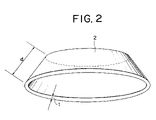
FIG. 2 is a perspective view of a doughnut-shaped electrode;
FIG. 3 is a schematic plan view of the doughnut-shaped electrode together with the movements of the spinning plate to the doughnut-shaped electrode;
FIG. 4 is a longitudinal cross sectional diagram of the system of a second embodiment of the present invention; and
FIG. 5 is a longitudinal cross sectional diagram of the conventional system.
DESCRIPTION OF THE PREFERRED EMBODIMENTS
Hereinafter, preferred embodiments will be explained according to the attached drawings. Through the explanation of the embodiments, the details of the present invention will be clarified.
In accordance with FIGS. 1-3 the first embodiment of the present invention is explained. FIG. 1 shows a longitudinal cross sectional diagram of the first embodiment of the plasma-assisted sputter deposition system of the present invention. The reactor 1 is provided with an electrode 2 arranged on its ceiling wall 1A and a wafer holder 5 arranged on its bottom plate 17. An upper-side support wall 1B supports the ceiling wall 1A. The ceiling wall 1A has a ring-shaped angled peripheral section. The electrode 2 is placed in the ring-shaped angled peripheral section of the ceiling wall 1A.
The electrode 2 is made of a metal such as Al, Ti, Ta etc. that is sputtered and deposited on a wafer 9 placed on the wafer holder 5. The electrode 2 is electrically isolated from the reactor 1 using a dielectric material 8. The electrode 2 is connected to a DC electric power source 10.
In the reactor 1 of the first embodiment, the electrode 2 is of a doughnut-shape or circular ring-shape, and there are gas inlets 6 at the bottom plate 17 and a gas outlet 7 at the lower section of the side wall 20 near the bottom plate 17. In the space at back of the electrode 2 there is a spinning plate or disk 3 to which a magnet arrangement 4 is attached.
The electrode 2 is made of a material that is sputtered and deposited on the wafer 9. The shape of the electrode 2 is circular with a hole in the center as shown in FIG. 2. The inner and outer diameters of the electrode 2 are not critical and decided by considering the wafer diameter and height from the wafer to the electrode 2. The centers of inner and outer diameters of the electrode 2 and the center of wafer 9 lie on the same straight line. The surfaces of electrode 2 are angled such that extension of these surfaces makes a conical-shape structure. The angle between the electrode surface and a horizontal line, which is denoted by “α” in FIG. 1 is not critical and generally smaller than 45°. One can also use a case that α is equal to 0, that is, that the electrode surface is parallel to the wafer surface. The thickness of the electrode 2 denoted by “t” in FIG. 2 is also not critical and can lie in the range of 2 mm to 20 mm. A thinner electrode 2 is preferable as it yields a higher magnetic flux on its lower surface. The electrode 2 is covered by an insulating material 8 in order to electrically isolate from the rest of the parts of the reactor 1 and is given a DC or rf electrical power. As one example, a DC power source 10 is shown in FIG. 1.
The magnet arrangement 4 comprised of a plurality of magnets is fixed to the spinning plate 3. The spinning plate 3 is usually made of a metal. The diameter of the spinning plate 3 is usually taken slightly shorter than the width of the electrode 2 denoted by “d” in FIG. 2. However, one can employ the spinning plate larger than the electrode width “d” with suitable hardware modifications.
The spinning plate 3 constantly spins on its central axis 16. In addition, the spinning plate 3 with the magnet arrangement 4 moves on a circular path above the electrode 2 similar to planetary motion. In this case, the spinning plate 3 is parallel to the surface of the doughnut-shaped electrode 2. These motions are schematically shown in FIG. 3. In FIG. 3, an arrow mark 31 denotes the spin motion and an arrow mark 32 denotes the planetary motion. A mechanism for making the spin motion and the planetary motion is comprised of a motor 33 connected to the central axis 16, a ring-shape guide member with a gear mechanism fixed to the side-wall 20 of the upper-side support wall 1B, and an connecting member for connecting the motor 33 and the ring-shaped guide member 34. When the motor 33 operates, the central axis 35 is rotated and the unit including the motor 33 and the spinning plate 3 is moved along the ring-shaped guide member 34 through the gear mechanism.
The magnet arrangement 4 below the spinning plate 3 is not critical and may be any symmetric or asymmetric magnet arrangement.
The wafer holder 5 is fixed to the bottom plate 17. It is comprised of a metal electrode 11, an electric static chuck (ESC) 12 or a thin dielectric layer 12, and an insulator 13. The metal electrode 11 is supplied with a temperature-controlled liquid via a liquid inlet 14 and an outlet 15. The temperature-controlled liquid is used to maintain a constant temperate usually in the range of 100° C. to −100° C. on the metal electrode 11. If a higher temperature, generally over 100° C. is needed, one can fix an electrical heating system within the metal electrode 11. There is the thin dielectric layer 12 on the upper surface of metal electrode to form the ESC. Within this dielectric layer 12 there may be very thin metal electrode or electrodes as a part of the ESC. Again, there may be a gas feeding mechanism to the ESC in order to increase the thermal conductivity between the wafer 9 and the ESC. Detailed explanation of the configuration of the ESC is not given as it commonly available in literature. The wafer holder 5 is fixed on the bottom plate 17 of the reactor 1. This eases making electrical wiring and cooling/heating mechanisms. However, one can make the wafer holder 5 movable in the vertical direction with the all facilities mentioned-above. The important feature of the wafer holder 5, compared to that explained in prior art, is that the wafer and the wafer holder are at rest during the film deposition. That is there are no any rotating parts of the wafer holder 5.
The operation of the above-mentioned structure is explained. The wafer 9 which is introduced into the reactor 1 through a wafer in/out door 18 is placed on the fixed wafer holder 5. The wafer 9 in the wafer holder 5 is electrostatically clamped on the ESC. The ESC is maintained to be a constant temperature with the assist of coolant or a heater. A gas is fed into the reactor 1 and the reactor is maintained a desired pressure. The pressure inside the reactor 1 is not critical and can be vary in the range of 0.1 mTorr to 100 mTorr. A DC electrical power is applied to the electrode 2 from the DC power source 10 to initiate and maintain plasma. The electric power of the DC current applied to the electrode 2 is not important and is decided by the required deposition rate and other parameters. If a lower deposition rate is required, a lower power, for example 100 W, is applied. Specially, when a precise control of the film thickness is needed, the deposition has to be done at a lower rate, for example 10 nm/min. In this case a lower DC power, for example 50 W, is applied to the electrode 2. Even though the whole electrode 2 is subjected to the same negative voltage applied by the DC power source 10, the plasma is concentrated below the spinning plate 3 since plasma is confined by the magnetic field. This dense plasma moves on a circular path below the electrode 2 with the movement of the spinning plate 3 with magnet arrangement 4. The sputtering is mainly occurred at the place where the dense plasma is and the sputtered atoms reach the wafer surface with angles. Therefore, the film deposition process is almost similar to that explain in the prior art section resulting in a film with a very good film uniformity.
The metal electrode 11 in the wafer holder 5 may or may not be given an rf current. Even if a rf power is applied the power of the rf current from a rf power source 36 is usually kept a lower value so that there is no excessive sputtering of the deposited film.
The sputtering system of the first embodiment yields extremely uniform films with the controllability of film thickness with a great accuracy while the wafer temperature can be maintained at any desired value. Further, deposition can be performed with the soft-ion bombardment or with re-sputtering processes.
In accordance with the first embodiment, the wafer holder 5 is at rest and the plasma produced at a region under the electrode 2, which corresponds to the magnet arrangement 4 of the spin plate 3, is rotated together with the planetary movement (revolution) of the spin plate 3. Therefore, even if the wafer holder 5 is not rotated, the uniform thin film is deposited onto the wafer 9 on the wafer holder 5.
Next, the second embodiment is explained with reference to FIG. 4. It is a slight modification of the first embodiment. The only modification in this system, compared to the first embodiment, is to use new structure of magnet arrangement corresponding to the magnet arrangement 4 without the above spinning plate 3. Here, two or more circular magnets 19 a and 19 b are placed on the outside surface of the electrode 2, which have alternate polarities facing the electrode surface. They are not moved. A configuration with the two circular magnets 19 a and 19 b is shown in FIG. 4, for example. These two magnets 19 a and 19 b are permanently fixed on the electrode or placed with a small separation, for example 1 mm, with the electrode and slightly moved parallel to electrode surface. There are magnetic flux lines 37 between the two circular magnets 19 a and 19 b. The magnetic flux lines 37 penetrate the electrode 2 into the inside of reactor 1. The slight movement of the circular magnets 19 a and 19 b results in an improvement of electrode utilization efficiency.
The application of the DC power or rf power source to the electrode 2 is same as that explained in the first embodiment. However, with the magnet arrangement strong doughnut-shape plasma is generated below the electrode 2 and the sputtering happens over a doughnut shape surface at the same time. Therefore, with this configuration, the deposition rate gets increased.
Except the above-mentioned changes, all the other structure, functions, procedures and results are the same as that explained in the first embodiment.
The present invention is used for plasma-assisted magnetron sputtering without rotating the wafer holder, and useful for depositing films on the wafer with film uniformity and thickness controllability, and a temperature-controllable in the wafer holder.
The configurations, shapes, sizes, and relative arrangements explained in the above embodiments are only generally shown to an extent enabling the present invention to be understood and worked. Further, the numerical values and compositions (materials) of the configurations are only illustrations. Therefore, the present invention is not limited to the embodiments explained above and can be modified in various ways so long as not departing from the scope of the technical idea shown in the claims.
The present disclosure relates to subject matter contained in Japanese Patent Application No. 2004-5866 filed on Jan. 13, 2004, and Japanese Patent Application No. 2004-99398 filed on Mar. 30, 2004, the disclosures of which are expressly incorporated herein by references in its entirety.
Although only preferred embodiments are specifically illustrated and described herein, it will be appreciated that many modifications and variations of the present invention are possible in light of the above teachings and within the purview of the appended claims without departing from the spirit and intended scope of the invention.

Claims (13)

1. A plasma-assisted sputter deposition system comprising:
a reactor into which a process gas is introduced to be used for producing plasma,
a doughnut-shaped electrode made of a material for sputtering by said plasma, wherein a lower surface of said doughnut-shaped electrode is angled to a surface of a wafer,
a spinning plate that spins on its central axis while moving in a circular path with respect to the central axis of the doughnut-shaped electrode above the doughnut-shaped electrode, wherein said spinning plate contains a magnet arrangement attached to its lower surface and is parallel to the angled side surface of said doughnut-shaped electrode,
a mechanism configured to have a motor connected to a central axis of said spinning plate, a ring-shaped guide member with gear mechanism fixed to a side wall of said reactor, and a connection member for connecting said motor and said ring-shaped guide member, for spinning said spinning plate on its central axis by the operation of said motor and moving said spinning plate above said doughnut-shaped electrode and along said ring-shaped guide member around the central axis of said doughnut-shaped electrode through said gear mechanism of said ring-shaped guide member by the operation of said motor,
an electrical power source connected to said doughnut-shaped electrode, and
a wafer holder for placing said wafer for film deposition, which is at rest during the film deposition.
2. The plasma-assisted sputter deposition system as claimed in claim 1, wherein said magnet arrangement on the lower surface of said spinning plate is symmetric around its spinning axis.
3. The plasma-assisted sputter deposition system as claimed in claim 1, wherein said magnet arrangement on the lower surface of spinning plate is asymmetric around its spinning axis.
4. A plasma-assisted sputter deposition system comprising:
a reactor in which plasma is produced by a process gas,
a circular target electrode made of a material sputtered by said plasma, having a hole at a center and a side surface angled to a surface of a wafer,
a spinning plate having a magnet arrangement and being placed over the side surface of said circular target electrode,
an electrical power source connected to said circular target electrode,
a wafer holder for placing said wafer for film deposition, which is at rest during the film deposition, and
a mechanism configured to have a motor connected to a central axis of said spinning plate, a ring-shaped guide member with gear mechanism fixed to a side wall of said reactor, and a connection member for connecting said motor and said ring-shaped guide member, for spinning said spinning plate on the central axis by the operation of said motor and moving said spinning plate above said circular target electrode and along said ring-shaped guide member around the central axis of said circular target electrode through said gear mechanism of said ring-shaped guide member by the operation of said motor.
5. The plasma-assisted sputter deposition system as claimed in claim 4, wherein said magnet arrangement on said spinning plate is symmetric around its spinning axis.
6. The plasma-assisted sputter deposition system as claimed in claim 4, wherein said magnet arrangement on said spinning plate is asymmetric around its spinning axis.
7. The plasma-assisted sputter deposition system as claimed in claim 4, wherein said magnet arrangement facing to said circular target electrode and having at least two circular magnets with different poles and different diameters which is placed over said circular target electrode, in order to generate one or more loop magnetic fluxes under said circular target electrode.
8. The plasma-assisted sputter deposition system as claimed in claim 1, wherein the thickness of said target electrode ranges from 2 mm to 20 mm.
9. The plasma-assisted sputter deposition system as claimed in claim 1, wherein said target electrode is electrically isolated from said reactor by dielectric materials.
10. The plasma-assisted sputter deposition system as claimed in claim 1, wherein a diameter of said spinning plate is smaller than the width of said target electrode.
11. The plasma-assisted sputter deposition system as claimed in claim 4 wherein the thickness of said target electrode ranges from 2 mm to 20 mm.
12. The plasma-assisted sputter deposition system as claimed in claim 4 wherein said target electrode is electrically isolated from said reactor by dielectric materials.
13. The plasma-assisted sputter deposition system as claimed in claim 4 wherein a diameter of said spinning plate is smaller than the width of said target electrode.
US10/905,574 2004-01-13 2005-01-11 Plasma-assisted sputter deposition system Expired - Fee Related US7625472B2 (en)

Applications Claiming Priority (4)

Application Number Priority Date Filing Date Title
JP2004005866 2004-01-13
JP2004-5866 2004-01-13
JP2004-99398 2004-03-30
JP2004099398A JP4541014B2 (en) 2004-01-13 2004-03-30 Plasma assisted sputter deposition system

Publications (2)

Publication Number Publication Date
US20050150457A1 US20050150457A1 (en) 2005-07-14
US7625472B2 true US7625472B2 (en) 2009-12-01

Family

ID=34197279

Family Applications (1)

Application Number Title Priority Date Filing Date
US10/905,574 Expired - Fee Related US7625472B2 (en) 2004-01-13 2005-01-11 Plasma-assisted sputter deposition system

Country Status (6)

Country Link
US (1) US7625472B2 (en)
JP (1) JP4541014B2 (en)
KR (1) KR20050074334A (en)
FR (1) FR2880632B1 (en)
GB (1) GB2410034B (en)
TW (1) TW200523394A (en)

Cited By (1)

* Cited by examiner, † Cited by third party
Publication number Priority date Publication date Assignee Title
US20130264308A1 (en) * 2012-04-04 2013-10-10 Taiwan Semiconductor Manufacturing Company, Ltd. Plasma process, film deposition method and system using rotary chuck

Families Citing this family (3)

* Cited by examiner, † Cited by third party
Publication number Priority date Publication date Assignee Title
JP2006037127A (en) * 2004-07-23 2006-02-09 Cyg Gijutsu Kenkyusho Kk Sputter electrode structure
JP6423290B2 (en) * 2015-03-06 2018-11-14 東京エレクトロン株式会社 Deposition equipment
KR102355296B1 (en) * 2017-08-08 2022-01-25 삼성전자주식회사 Semiconductor Memory Device and Apparatus for manufacturing the Same

Citations (17)

* Cited by examiner, † Cited by third party
Publication number Priority date Publication date Assignee Title
US4282083A (en) * 1979-02-19 1981-08-04 Hirada Stechnikai Ipari Kutato Intezet Penning sputter source
US5126029A (en) 1990-12-27 1992-06-30 Intel Corporation Apparatus and method for achieving via step coverage symmetry
JPH05189762A (en) 1992-01-09 1993-07-30 Hitachi Ltd Process and apparatus for production of magnetic recording medium
US5378341A (en) 1993-10-13 1995-01-03 The United States Of America As Represented By The Secretary Of The Air Force Conical magnetron sputter source
JPH07126847A (en) 1993-10-29 1995-05-16 Shin Etsu Chem Co Ltd Formation of electrode magnetic field for sputtering
EP0853330A2 (en) 1997-01-14 1998-07-15 Applied Materials, Inc. Ionized PVD source to produce uniform low-particle deposition
US5944968A (en) 1996-09-18 1999-08-31 Anelva Corporation Sputtering apparatus
US6238528B1 (en) * 1998-10-13 2001-05-29 Applied Materials, Inc. Plasma density modulator for improved plasma density uniformity and thickness uniformity in an ionized metal plasma source
WO2001053562A1 (en) 2000-01-19 2001-07-26 Glocker David A Conical sputtering target
US6287435B1 (en) 1998-05-06 2001-09-11 Tokyo Electron Limited Method and apparatus for ionized physical vapor deposition
US20020064595A1 (en) 2000-11-30 2002-05-30 Shuji Nomura Magnetic multi-layer film manufacturing apparatus
US6432286B1 (en) 1998-06-10 2002-08-13 David A. Glocker Conical sputtering target
JP2002296413A (en) 2001-03-29 2002-10-09 Anelva Corp Apparatus and method for manufacturing optical multilayered film interference filter
US20030079984A1 (en) * 2001-10-30 2003-05-01 Kenji Okatani Sputtering apparatus and film forming method
US6613199B1 (en) 2001-10-25 2003-09-02 Novellus Systems, Inc. Apparatus and method for physical vapor deposition using an open top hollow cathode magnetron
WO2003100819A1 (en) 2002-05-21 2003-12-04 Applied Materials, Inc. Planetary magnetron
US6841050B2 (en) * 2002-05-21 2005-01-11 Applied Materials, Inc. Small planetary magnetron

Family Cites Families (3)

* Cited by examiner, † Cited by third party
Publication number Priority date Publication date Assignee Title
JPS6217175A (en) * 1985-07-16 1987-01-26 Nissin Electric Co Ltd Sputtering device
JPH02111878A (en) * 1988-10-20 1990-04-24 Fuji Photo Film Co Ltd Sputtering device
JPH051373A (en) * 1991-03-25 1993-01-08 Shin Meiwa Ind Co Ltd Sputtering system

Patent Citations (20)

* Cited by examiner, † Cited by third party
Publication number Priority date Publication date Assignee Title
US4282083A (en) * 1979-02-19 1981-08-04 Hirada Stechnikai Ipari Kutato Intezet Penning sputter source
US5126029A (en) 1990-12-27 1992-06-30 Intel Corporation Apparatus and method for achieving via step coverage symmetry
JPH05189762A (en) 1992-01-09 1993-07-30 Hitachi Ltd Process and apparatus for production of magnetic recording medium
US5378341A (en) 1993-10-13 1995-01-03 The United States Of America As Represented By The Secretary Of The Air Force Conical magnetron sputter source
JPH07126847A (en) 1993-10-29 1995-05-16 Shin Etsu Chem Co Ltd Formation of electrode magnetic field for sputtering
US5944968A (en) 1996-09-18 1999-08-31 Anelva Corporation Sputtering apparatus
EP0853330A2 (en) 1997-01-14 1998-07-15 Applied Materials, Inc. Ionized PVD source to produce uniform low-particle deposition
JPH10212573A (en) 1997-01-14 1998-08-11 Applied Materials Inc Ionized pvd source to generate uniform low particle deposition
US6287435B1 (en) 1998-05-06 2001-09-11 Tokyo Electron Limited Method and apparatus for ionized physical vapor deposition
US6432286B1 (en) 1998-06-10 2002-08-13 David A. Glocker Conical sputtering target
US6238528B1 (en) * 1998-10-13 2001-05-29 Applied Materials, Inc. Plasma density modulator for improved plasma density uniformity and thickness uniformity in an ionized metal plasma source
US6458252B1 (en) * 1999-11-18 2002-10-01 Tokyo Electron Limited High target utilization magnetic arrangement for a truncated conical sputtering target
WO2001053562A1 (en) 2000-01-19 2001-07-26 Glocker David A Conical sputtering target
US20020064595A1 (en) 2000-11-30 2002-05-30 Shuji Nomura Magnetic multi-layer film manufacturing apparatus
JP2002167661A (en) 2000-11-30 2002-06-11 Anelva Corp Magnetic multilayered film deposition system
JP2002296413A (en) 2001-03-29 2002-10-09 Anelva Corp Apparatus and method for manufacturing optical multilayered film interference filter
US6613199B1 (en) 2001-10-25 2003-09-02 Novellus Systems, Inc. Apparatus and method for physical vapor deposition using an open top hollow cathode magnetron
US20030079984A1 (en) * 2001-10-30 2003-05-01 Kenji Okatani Sputtering apparatus and film forming method
WO2003100819A1 (en) 2002-05-21 2003-12-04 Applied Materials, Inc. Planetary magnetron
US6841050B2 (en) * 2002-05-21 2005-01-11 Applied Materials, Inc. Small planetary magnetron

Non-Patent Citations (2)

* Cited by examiner, † Cited by third party
Title
British Search Report Application No. GB 0500118.5, dated Apr. 12, 2005.
English language translation of a Japanese Office Action received on Aug. 21, 2009 in corresponding Japanese Patent Application No. 2004-099398.

Cited By (2)

* Cited by examiner, † Cited by third party
Publication number Priority date Publication date Assignee Title
US20130264308A1 (en) * 2012-04-04 2013-10-10 Taiwan Semiconductor Manufacturing Company, Ltd. Plasma process, film deposition method and system using rotary chuck
US8920888B2 (en) * 2012-04-04 2014-12-30 Taiwan Semiconductor Manufacturing Company, Ltd. Plasma process, film deposition method and system using rotary chuck

Also Published As

Publication number Publication date
TW200523394A (en) 2005-07-16
US20050150457A1 (en) 2005-07-14
FR2880632A1 (en) 2006-07-14
JP2005226153A (en) 2005-08-25
KR20050074334A (en) 2005-07-18
GB2410034B (en) 2008-06-11
FR2880632B1 (en) 2007-11-23
JP4541014B2 (en) 2010-09-08
GB0500118D0 (en) 2005-02-09
GB2410034A (en) 2005-07-20

Similar Documents

Publication Publication Date Title
US6506290B1 (en) Sputtering apparatus with magnetron device
US6228236B1 (en) Sputter magnetron having two rotation diameters
US5334302A (en) Magnetron sputtering apparatus and sputtering gun for use in the same
US6113752A (en) Method and device for coating substrate
US8906208B2 (en) Sputtering apparatus, sputtering method, and electronic device manufacturing method
US8956512B2 (en) Magnetron sputtering apparatus and film forming method
JPH01272765A (en) Sputtering coating apparatus and method
KR20080059304A (en) Film forming apparatus method of forming film
GB2411290A (en) Wafer stage for holding a wafer in a plasma chamber
US7625472B2 (en) Plasma-assisted sputter deposition system
JP2011179119A (en) Apparatus and method of physical vapor deposition with heat diffuser
JP2004162138A (en) Plasma assisted sputtering film-forming apparatus
JPH10152772A (en) Sputtering method and apparatus therefor
JP2009299191A (en) Plasma-assisted sputter film-forming apparatus
JPH11302841A (en) Sputtering system
JP3056222B2 (en) Sputtering apparatus and sputtering method
GB2440256A (en) Plasma assisted sputter deposition.
JP2000319780A (en) Sputtering cathode and magnetron type sputtering device equipped with the same
WO2018095514A1 (en) Apparatus and method for layer deposition on a substrate
JPH11340165A (en) Sputtering device and magnetron unit
JP7438853B2 (en) Magnetron sputtering equipment
JPH04371575A (en) Sputtering device
US20190172690A1 (en) Substrate processing apparatus
JPH01116068A (en) Bias sputtering device
JPH02298263A (en) Sputtering device

Legal Events

Date Code Title Description
AS Assignment

Owner name: ANELVA CORPORATION, JAPAN

Free format text: ASSIGNMENT OF ASSIGNORS INTEREST;ASSIGNOR:WICKRAMANAYAKA, SUNIL;REEL/FRAME:015551/0601

Effective date: 20050106

AS Assignment

Owner name: CANON ANELVA CORPORATION, JAPAN

Free format text: CHANGE OF NAME;ASSIGNOR:ANELVA CORPORATION;REEL/FRAME:021701/0140

Effective date: 20051001

Owner name: CANON ANELVA CORPORATION,JAPAN

Free format text: CHANGE OF NAME;ASSIGNOR:ANELVA CORPORATION;REEL/FRAME:021701/0140

Effective date: 20051001

FEPP Fee payment procedure

Free format text: PAYOR NUMBER ASSIGNED (ORIGINAL EVENT CODE: ASPN); ENTITY STATUS OF PATENT OWNER: LARGE ENTITY

CC Certificate of correction
REMI Maintenance fee reminder mailed
LAPS Lapse for failure to pay maintenance fees
STCH Information on status: patent discontinuation

Free format text: PATENT EXPIRED DUE TO NONPAYMENT OF MAINTENANCE FEES UNDER 37 CFR 1.362

FP Lapsed due to failure to pay maintenance fee

Effective date: 20131201