US7547582B2 - Method of fabricating a surface adapting cap with integral adapting material for single and multi chip assemblies - Google Patents
Method of fabricating a surface adapting cap with integral adapting material for single and multi chip assemblies Download PDFInfo
- Publication number
- US7547582B2 US7547582B2 US11/535,091 US53509106A US7547582B2 US 7547582 B2 US7547582 B2 US 7547582B2 US 53509106 A US53509106 A US 53509106A US 7547582 B2 US7547582 B2 US 7547582B2
- Authority
- US
- United States
- Prior art keywords
- chip
- cap
- membrane
- adaptive
- adapting
- Prior art date
- Legal status (The legal status is an assumption and is not a legal conclusion. Google has not performed a legal analysis and makes no representation as to the accuracy of the status listed.)
- Expired - Fee Related, expires
Links
Images


Classifications
-
- H—ELECTRICITY
- H10—SEMICONDUCTOR DEVICES; ELECTRIC SOLID-STATE DEVICES NOT OTHERWISE PROVIDED FOR
- H10W—GENERIC PACKAGES, INTERCONNECTIONS, CONNECTORS OR OTHER CONSTRUCTIONAL DETAILS OF DEVICES COVERED BY CLASS H10
- H10W40/00—Arrangements for thermal protection or thermal control
- H10W40/70—Fillings or auxiliary members in containers or in encapsulations for thermal protection or control
- H10W40/77—Auxiliary members characterised by their shape
-
- H—ELECTRICITY
- H10—SEMICONDUCTOR DEVICES; ELECTRIC SOLID-STATE DEVICES NOT OTHERWISE PROVIDED FOR
- H10D—INORGANIC ELECTRIC SEMICONDUCTOR DEVICES
- H10D62/00—Semiconductor bodies, or regions thereof, of devices having potential barriers
- H10D62/10—Shapes, relative sizes or dispositions of the regions of the semiconductor bodies; Shapes of the semiconductor bodies
- H10D62/117—Shapes of semiconductor bodies
-
- H—ELECTRICITY
- H10—SEMICONDUCTOR DEVICES; ELECTRIC SOLID-STATE DEVICES NOT OTHERWISE PROVIDED FOR
- H10W—GENERIC PACKAGES, INTERCONNECTIONS, CONNECTORS OR OTHER CONSTRUCTIONAL DETAILS OF DEVICES COVERED BY CLASS H10
- H10W72/00—Interconnections or connectors in packages
- H10W72/071—Connecting or disconnecting
- H10W72/072—Connecting or disconnecting of bump connectors
- H10W72/07251—Connecting or disconnecting of bump connectors characterised by changes in properties of the bump connectors during connecting
-
- H—ELECTRICITY
- H10—SEMICONDUCTOR DEVICES; ELECTRIC SOLID-STATE DEVICES NOT OTHERWISE PROVIDED FOR
- H10W—GENERIC PACKAGES, INTERCONNECTIONS, CONNECTORS OR OTHER CONSTRUCTIONAL DETAILS OF DEVICES COVERED BY CLASS H10
- H10W72/00—Interconnections or connectors in packages
- H10W72/20—Bump connectors, e.g. solder bumps or copper pillars; Dummy bumps; Thermal bumps
-
- H—ELECTRICITY
- H10—SEMICONDUCTOR DEVICES; ELECTRIC SOLID-STATE DEVICES NOT OTHERWISE PROVIDED FOR
- H10W—GENERIC PACKAGES, INTERCONNECTIONS, CONNECTORS OR OTHER CONSTRUCTIONAL DETAILS OF DEVICES COVERED BY CLASS H10
- H10W72/00—Interconnections or connectors in packages
- H10W72/851—Dispositions of multiple connectors or interconnections
- H10W72/874—On different surfaces
- H10W72/877—Bump connectors and die-attach connectors
Definitions
- the present invention relates to an improved surface adapting cap with an integrated adapting thermally conductive material on one or more semiconductor chips in single and multi chip modules.
- the present invention is related to semiconductor device manufacturing technology, and in particular to the integrated circuit (IC) packaging.
- Semiconductor device manufacturing technology is continually being pushed to higher levels of density and speed, with the objective of offering ever increasing functionality in a single package. This trend is resulting in sharply increasing power densities that demand continuous improvements in cooling efficiency.
- the introduction of multichip modules has intensified the need for efficient cooling even further by creating a more complex thermal environment.
- the Controlled Collapse Chip Connection (C4) protocol has emerged as the dominant assembly process for semiconductor chips in the Single Chip Module (SCM) and multichip Module (MCM) assembly process. In this assembly process each chip is inverted (or “flipped”) and bonded both electrically and mechanically at each connecting interface to conductive elements on a supporting substrate.
- the cooling mechanism is attached to the exposed upper surface (or “bottom”) of each chip through a thermal interface.
- the primary factor in determining the efficiency of the cooling mechanism is the effectiveness of this thermal interface resistance.
- a reduction in thermal interface resistance produces a significant improvement in the overall thermal performance.
- the thermal interface material comprises thermally conductive material (such as grease, adhesive, solder etc) that thermally connects the chip to the enclosing cap or sealing structure of the module.
- thermally conductive material such as grease, adhesive, solder etc
- the gap thickness is partially determined by the tolerances of the production process that range from about 60 ⁇ m to 12 ⁇ m dependent on the packaging system. This tolerance is caused by warpage of the chip, as well as position and angular tolerances in the placement of each chip. The trend towards ever reducing interface material thickness greatly enhances the significance of these variations.
- U.S. Pat. No. 6,637,506 describes an apparatus for enhancing the thermal match between the parts of packaged semiconductor devices. It describes a heat spreader that is in thermal contact with a die and specifies the matching of the thermal expansion of a chip and the heat spreader by confining to a center portion of the heat spreader within the perimeter portion.
- the perimeter portion of the heat spreader is selected from the group of material with a lower thermal expansion coefficient (CTE) than the material for the center portion of the heat spreader.
- CTE thermal expansion coefficient
- U.S. Pat. No. 6,292,369 teaches lid structures and packaging modules having improved heat dissipation whose performance is characterized by a customized lid understructure to enable a reduction in the amount of compliant thermally conductive material in the primary heat dissipation path, wherein the understructure is customized according to the chip(s) that are to be housed.
- the customization is achieved by the use of shims and a deformable lid understructure.
- This understructure is not capable of providing enough pressure for a low viscosity medium to adapt to convex and concave chip warpage as it does not seal the deformable structure at the periphery.
- the present invention aims to mitigate the above-mentioned problems and endeavours to provide a solution for maintaining the gap uniformity between chip and cap for single chip module (SCM) and multi chip modules (MCM) in the presence of chip warpage and variation in chip placement.
- SCM single chip module
- MCM multi chip modules
- the aim of the present invention is to provide a method and an apparatus to accommodate chip warping, position and angle tolerances for single and multi chip module.
- Another object of the invention is to reduce the gap tolerance between the semiconductor chip and cap and hence to increase the thermal performances by maintaining a constant gap thickness at every chip position and for every chip on the module thus compensating for the tolerances caused by variabilities in the cold plate, chip fabrication and in the controlled collapse chip connection (C4) soldering protocol.
- C4 controlled collapse chip connection
- a surface adapting thermal interface between chip and enclosing structure or cap for single and multi chip module assembly comprising:
- the solution provided by the adaption material is capable of reducing gap thickness but requires changes in cap assembly and its attachment process supporting the semiconductor chip.
- the proposed system also allows full reworkability.
- FIG. 1 shows the typical deviations from co-planarity in multi chip module (MCM).
- FIG. 2 shows the trend of thermal interface resistance and interface thickness.
- FIG. 3 shows a previously-proposed method.
- FIG. 4 shows small gap technology
- FIG. 5 shows an embodiment of the present invention for single chip module (SCM) and multi chip module (MCM).
- SCM single chip module
- MCM multi chip module
- FIG. 6 shows a plot of the reduction of thermal resistance of the adaptive interface in single chip module (SCM) in accordance with an embodiment of the present invention.
- FIG. 7 shows a plot of the variation in thermal resistance with change in gap thickness for chip(s) in multi chip module (MCM) in accordance with an embodiment of the present invention.
- FIG. 8 shows one of the embodiments in accordance with the present invention for accommodating z-position tolerance as well.
- FIG. 9 shows one of the embodiments for capless module in accordance with the present invention.
- FIG. 10 shows another embodiment of the present invention, which utilizes highly elastic and low stiffness integrated membrane that is removed prior to the application of thermal interface material.
- FIGS. 11A and 11B shows other embodiments in accordance with the present invention comprising closed or open air pockets which act as reservoirs and deliver the needed backpressure to the viscous medium.
- FIG. 12 shows the extension in FIG. 11 of the present invention in accordance with the present invention with multiple reservoir structure and adhesion controlled brake joints.
- FIG. 13 shows the possible manufacturing process as explained in above mentioned FIGS. 5-12 .
- FIG. 14 expands the previously described adaptation method to dynamic adaptation method.
- FIG. 15 shows another embodiment in accordance with the present invention comprising flexile manifold and jet membrane.
- FIG. 16 shows another embodiment in accordance with the present invention as explained in FIG. 15 comprising flexile jet membrane.
- An embodiment of the present invention provides an adaptive material integral to the cap that adapts to the warping and placement tolerances of the chip.
- FIG. 1 shows typical tolerances in multi chip module packing.
- cap bow 102 On the bottom side of the cap is a thermally conductive material integrated which adjusts for the non-uniformity between cap and chip and defines a constant and equal gap between chip and cap. This gap then gets filled with a compliant thermal interface material such as paste, gel or adhesive.
- FIG. 2 illustrates the variation in thermal resistance as a function of interface thickness for different paste materials with the arrow showing the current trend towards smaller and smaller gaps.
- the ratio between the gap thickness and the thermal resistance is related to the bulk conductivity of the material. Materials on the lower right have high bulk conductivity while materials on the upper left have low bulk conductivity.
- FIG. 3 shows a previously-proposed method used to adapt to the surface of the chip, where non-planarity of the cap 306 is allowed up to about 12 ⁇ m and when the bowing of the chip 307 is 10 ⁇ m and a solder foil 302 and a membrane foil 304 are positioned between cap 303 and chip 301 . The parts are precompressed with a force F.
- the above-described method includes the confinement of the adaptive material. This confinement allows the use of low viscous materials and allows reworkability. Another drawback of the method is the limited z-position tolerance due to the confinement of the adaptive material. In an embodiment of the present invention, the z-position tolerances are taken into account.
- FIG. 4 shows a method, which reduces the variation in thermal interface gap caused by position and angle tolerances of the chips on multi chip modules. This technology is called small gap technology and produces lower mean values and half as much variation in the thermal resistance from chip to chip and module to module.
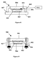
- FIG. 5 proposes a method which may adapt to chip warpages as high as 60 ⁇ m. This technique further improves the mean value and the variations of the paste gap 505 .
- Device cap 501 with integrated membrane 503 includes a buried, confined, high thermal conductivity adapting material with liquidus temperature slightly above the chip operating temperature or with. a possible solidification by a curing step.
- the membrane 503 may be made utilizing metal such as copper, which is highly flexible and can be surrounded by ridge 502 .
- the cap 501 is preassembled to the chip 504 at a temperature above liquidus or below curing temperature of the buried adapting material.
- FIG. 6 shows the reduction factor of the maximal thermal resistance of the thermal interface material 505 in comparison with a non-adaptive cap for single chip module (SCM) as a function of the residual gap reached after the paste squeeze accounting for the reduced thermal conductivity of the adapting material 506 compared to copper for the following parameters:
- FIG. 7 shows the reduction factor of the thermal resistance in multi chip module (MCM) as function of the gap thickness in the paste above the chip(s). For gaps below 10 ⁇ m the improvement is 2.5 times which is higher than in a single chip module due to the additional position and angle tolerance from chip to chip in a MCM:
- FIG. 8 illustrates the side view of a device 800 in accordance with an embodiment of the present invention in which the chip 803 is attached to a substrate 801 through solder bumps 802 and the adaptive small gap technology pedestal 804 is coupled to the chip 803 through a thermal interface paste 806 .
- Annular extension(s) 805 shown extending beyond location 808 of pedestal 804 ) of the cap is attached to the substrate 801 with fastening material 807 to provide rigid support to the cap and enable overall stability.
- the integrated flexible membrane and the enclosed adaptive material 806 a surface non-parallelism, non-planarity and residual small z-variations are compensated with resulting uniformity improvement for the bondline thickness of the paste.
- capless modules 900 removal of the cap results in a reduced thermal resistance and hence in a better thermal performance.
- mechanical fixations 902 hold the heat sink 901 on top of the chips with a controlled normal force thus replacing the cap.
- Heat sink 901 is fixed to the substrate 903 through mechanical fixations 902 .
- Chip 905 is mounted to the substrate 903 via solder bumps 904 .
- Heat sink 901 is coupled to the chip 905 through thermal interface paste 906 with uniform bond line thickness, between heat sink 901 and chip 905 possible by the enclosed adaptive material 907 .
- FIG. 10 shows another embodiment of the present invention, in which cap 1001 utilizes a highly elastic and low stiffness integrated membrane 1003 surrounded by a ridge 1002 , containing the adaptive material 1005 .
- Membrane 1003 allows an increase in confinement volume with build up of the hydrostatic pressure (shown as F) owing to elastic strain, Due to the lack of thermally conductive, low Young's Modulus materials, the elastic foil is preferably a thermally resistant polymer and is preferably removed after the solder reflow process.
- the cap 1001 is pressed to the desired chip 1004 with a normal force and the temperature is increased above the liquidus temperature of the solder. After the reflow process the membrane is removed, a paste material 1006 is applied, arid the cap is pressed onto the chip.
- FIG. 11 shows yet another embodiment, where air pockets 1102 are provided that can accept excess solder 1104 during the reflow process.
- the whole compartment is sealed by the same membrane 1105 which may also act as a valve 1103 for flow control.
- the chip 1106 is compressed against the cap assembly 1101 , which results in the overflow of the surface adaptable material through air pockets 1107 for control of applied pressure within the adaptive material chamber.
- FIG.11B is yet another implementation showing chip 1113 , in which cap assembly 1115 , has surface adaptable material 1111 sealed by membrane 1112 with valve 1110 .
- Air pockets are used which have ports 1102 on the rear such that the pressure in the reservoir 1109 can be controlled by an external pressure gauge 1114 .
- FIG. 12 is an extension of FIG. 11A and FIG. 11B employing multiple confined reservoirs 1201 are created using defined adhesion bonds. Local delamination (shown at 1202 ) of these adhesion bonds at elevated hydrostatic pressure increases the volume for liquid adaptation.
- cap 1301 assembly consists of solder 1302 and integrated membrane 1303 .
- Solder 1302 consists of a preform foil, screen printed solder paste or electroplated material, while the integrated membrane 1303 comprises steps of electroplating, foil with roller bonding to the frame or sputtering.
- Valve 1305 is provided for flow control while air pocket 1304 accommodates any of the overflow that occurs.
- the adaptation method of the present invention can also be extended to a dynamic adaptation method.
- the system should have low stiffness during operation but still serving with a restoring force to deform the membrane elastically to the same actual chip warpage.
- the adaptation material should be a liquid or having low stiffness.
- Eutectic GalnSn which is liquid at room temperature, may be used. It may also be a phase changing material which is liquid below driving temperature.
- FIG. 14 shows a dynamic adaptive microchannel cold plate with a low stiffness material having gas enclosures 1401 , which allow a volumetric compression in supporting the fin structure 1402 attached to the base plate membrane 1403 .
- the coldplate is attached to the chip in a constant force mode which causes the membrane to adapt to the actual chip warpage.
- the pressure built up by the coolant which gets pumped around in a closed or open loop system causes the membrane 1403 to adapt dynamically the surface of the chip 1405 .
- FIG. 15 illustrates an alternative arrangement in which cap assembly 1503 (having ports 1501 , 1502 similar to those shown in FIG. 11B ) includes a low stiffness patterned sealing gasket 1504 that allows the dynamic adaptation of the flexible manifold 1505 including the jet membrane 1506 .
- the cap assembly 1601 may allow for dynamic adaptation of or just the jet membrane 1603 .
- spacers 1507 (or spacers 1604 ) on the chip 1508 (or chip 1605 ) define the needed gap between membrane 1506 (or membrane 1603 ) and chip 1508 (or chip 1605 ).
- This approach reduces abnormal flow distribution of liquid in the gap caused by surface bowing (gap tolerances) as explained in FIG. 1 . Therefore this approach allows a reduction in the gap thickness due to the smaller gap tolerance, which is advantageous in terms of the cooling performance of the semiconductor device.
Landscapes
- Cooling Or The Like Of Semiconductors Or Solid State Devices (AREA)
Abstract
Description
-
- a high thermal conductivity, mechanically deformable membrane integrated with or attached to the enclosing structure or cap to create an enclosed space bounded on all sides by said membrane and cap; and
- a high thermal conductivity material confined within said enclosed space, and having a softening temperature or melting point slightly above the chip operating temperature.
| Thermal conductivity of | 3 W/(m * K) |
| TIM material | |
| Bowing of cap and |
20 μm |
| z- |
0 μm |
| Residual bowing after |
5 |
| Solder thickness | |
| 30 μm | |
| Solder | InSn Tl = 118° C., 34 W/(m * K) |
| Bowing of cap and |
20 μm |
| z- |
25 μm |
| Residual bowing after |
5 μm |
| Solder thickness | 60 μm |
| Solder | InSn Tl = 118° C., 34 W/(m * K) |
Claims (5)
Priority Applications (1)
| Application Number | Priority Date | Filing Date | Title |
|---|---|---|---|
| US11/535,091 US7547582B2 (en) | 2006-09-26 | 2006-09-26 | Method of fabricating a surface adapting cap with integral adapting material for single and multi chip assemblies |
Applications Claiming Priority (1)
| Application Number | Priority Date | Filing Date | Title |
|---|---|---|---|
| US11/535,091 US7547582B2 (en) | 2006-09-26 | 2006-09-26 | Method of fabricating a surface adapting cap with integral adapting material for single and multi chip assemblies |
Publications (2)
| Publication Number | Publication Date |
|---|---|
| US20080073775A1 US20080073775A1 (en) | 2008-03-27 |
| US7547582B2 true US7547582B2 (en) | 2009-06-16 |
Family
ID=39224058
Family Applications (1)
| Application Number | Title | Priority Date | Filing Date |
|---|---|---|---|
| US11/535,091 Expired - Fee Related US7547582B2 (en) | 2006-09-26 | 2006-09-26 | Method of fabricating a surface adapting cap with integral adapting material for single and multi chip assemblies |
Country Status (1)
| Country | Link |
|---|---|
| US (1) | US7547582B2 (en) |
Cited By (17)
| Publication number | Priority date | Publication date | Assignee | Title |
|---|---|---|---|---|
| US20090296354A1 (en) * | 2008-05-30 | 2009-12-03 | Kabushiki Kaisha Toshiba | Electronic apparatus |
| US20100181665A1 (en) * | 2009-01-22 | 2010-07-22 | International Business Machines Corporation | System and Method of Achieving Mechanical and Thermal Stability in a Multi-Chip Package |
| US20110228482A1 (en) * | 2009-03-31 | 2011-09-22 | Apple Inc. | Method and apparatus for distributing a thermal interface material |
| US20120080785A1 (en) * | 2010-10-01 | 2012-04-05 | Raytheon Company | Semiconductor cooling apparatus |
| US20120309132A1 (en) * | 2007-09-19 | 2012-12-06 | International Business Machines Corporation | Curvilinear heat spreader/lid with improved heat dissipation |
| US8592970B2 (en) | 2011-06-27 | 2013-11-26 | International Business Machines Corporation | Multichip electronic packages and methods of manufacture |
| US8797741B2 (en) | 2010-10-21 | 2014-08-05 | Raytheon Company | Maintaining thermal uniformity in micro-channel cold plates with two-phase flows |
| US8823164B2 (en) | 2011-10-28 | 2014-09-02 | International Business Machines Corporation | Heatsink attachment module |
| US8900927B2 (en) | 2010-08-16 | 2014-12-02 | International Business Machines Corporation | Multichip electronic packages and methods of manufacture |
| CN104680004A (en) * | 2015-02-11 | 2015-06-03 | 西安建筑科技大学 | Building energy-saving rate calculation method |
| CN104680001A (en) * | 2015-02-11 | 2015-06-03 | 西安建筑科技大学 | Method for calculating architectural energy saving rate based on human body thermal adaptive model |
| US9153520B2 (en) | 2011-11-14 | 2015-10-06 | Micron Technology, Inc. | Stacked semiconductor die assemblies with multiple thermal paths and associated systems and methods |
| US9392731B2 (en) | 2013-11-18 | 2016-07-12 | Globalfoundries Inc. | Cooling apparatus with dynamic load adjustment |
| US20160263714A1 (en) * | 2012-09-29 | 2016-09-15 | Intel Corporation | Adjustable heat pipe thermal unit |
| US20190204023A1 (en) * | 2017-12-29 | 2019-07-04 | International Business Machines Corporation | Injection-molded flexible cold plate |
| US10551132B2 (en) | 2017-11-28 | 2020-02-04 | International Business Machines Corporation | Heat removal element with thermal expansion coefficient mismatch |
| US11058030B2 (en) | 2019-04-22 | 2021-07-06 | International Business Machines Corporation | Cold plate with flex regions between fin areas |
Families Citing this family (14)
| Publication number | Priority date | Publication date | Assignee | Title |
|---|---|---|---|---|
| JP2008153305A (en) * | 2006-12-14 | 2008-07-03 | Nec Electronics Corp | Semiconductor device |
| US20080142954A1 (en) * | 2006-12-19 | 2008-06-19 | Chuan Hu | Multi-chip package having two or more heat spreaders |
| US9006887B2 (en) | 2009-03-04 | 2015-04-14 | Intel Corporation | Forming sacrificial composite materials for package-on-package architectures and structures formed thereby |
| US20110096507A1 (en) * | 2009-10-24 | 2011-04-28 | Kester, Inc. | Microelectronic thermal interface |
| US9658000B2 (en) * | 2012-02-15 | 2017-05-23 | Abaco Systems, Inc. | Flexible metallic heat connector |
| US20150184053A1 (en) * | 2013-12-27 | 2015-07-02 | Shankar Krishnan | Gasketted thermal interface |
| US9615486B2 (en) * | 2014-03-26 | 2017-04-04 | General Electric Company | Thermal interface devices |
| US11282763B2 (en) * | 2019-06-24 | 2022-03-22 | Amkor Technology Singapore Holding Pte. Ltd. | Semiconductor device having a lid with through-holes |
| JP7051774B2 (en) * | 2019-09-25 | 2022-04-11 | 本田技研工業株式会社 | Heat dissipation structure of electrical component assembly, heat conduction sheet, manufacturing method of electrical component assembly |
| US11121053B2 (en) * | 2020-01-17 | 2021-09-14 | Asia Vital Components (China) Co., Ltd. | Die heat dissipation structure |
| US12014971B2 (en) * | 2021-06-01 | 2024-06-18 | Nxp Usa, Inc. | Thermal interface structures, electrical systems with thermal interface structures, and methods of manufacture thereof |
| CN116544153B (en) * | 2023-07-06 | 2023-09-01 | 成都汉芯国科集成技术有限公司 | 3D packaging system with heat dissipation interconnection function and packaging method thereof |
| CN119852254A (en) * | 2023-10-09 | 2025-04-18 | 沐曦集成电路(上海)股份有限公司 | Chip packaging heat dissipation cover and chip packaging structure |
| CN119852253A (en) * | 2023-10-09 | 2025-04-18 | 沐曦集成电路(上海)股份有限公司 | Substrate warpage inhibition structure and chip packaging structure |
Citations (7)
| Publication number | Priority date | Publication date | Assignee | Title |
|---|---|---|---|---|
| US4313492A (en) * | 1979-12-20 | 1982-02-02 | International Business Machines Corporation | Micro helix thermo capsule |
| US5729052A (en) * | 1996-06-20 | 1998-03-17 | International Business Machines Corporation | Integrated ULSI heatsink |
| US6292369B1 (en) | 2000-08-07 | 2001-09-18 | International Business Machines Corporation | Methods for customizing lid for improved thermal performance of modules using flip chips |
| US6637506B2 (en) * | 2002-03-08 | 2003-10-28 | Sun Microsystems, Inc. | Multi-material heat spreader |
| US20070127211A1 (en) * | 2004-12-03 | 2007-06-07 | Chris Macris | Liquid metal thermal interface material system |
| US20070137300A1 (en) * | 2005-12-20 | 2007-06-21 | Dwyer Paul W | Load beam for surface acoustic wave accelerometer |
| US20080137300A1 (en) * | 2005-10-11 | 2008-06-12 | Macris Chris G | Liquid metal thermal interface material system |
-
2006
- 2006-09-26 US US11/535,091 patent/US7547582B2/en not_active Expired - Fee Related
Patent Citations (7)
| Publication number | Priority date | Publication date | Assignee | Title |
|---|---|---|---|---|
| US4313492A (en) * | 1979-12-20 | 1982-02-02 | International Business Machines Corporation | Micro helix thermo capsule |
| US5729052A (en) * | 1996-06-20 | 1998-03-17 | International Business Machines Corporation | Integrated ULSI heatsink |
| US6292369B1 (en) | 2000-08-07 | 2001-09-18 | International Business Machines Corporation | Methods for customizing lid for improved thermal performance of modules using flip chips |
| US6637506B2 (en) * | 2002-03-08 | 2003-10-28 | Sun Microsystems, Inc. | Multi-material heat spreader |
| US20070127211A1 (en) * | 2004-12-03 | 2007-06-07 | Chris Macris | Liquid metal thermal interface material system |
| US20080137300A1 (en) * | 2005-10-11 | 2008-06-12 | Macris Chris G | Liquid metal thermal interface material system |
| US20070137300A1 (en) * | 2005-12-20 | 2007-06-21 | Dwyer Paul W | Load beam for surface acoustic wave accelerometer |
Cited By (36)
| Publication number | Priority date | Publication date | Assignee | Title |
|---|---|---|---|---|
| US20120309132A1 (en) * | 2007-09-19 | 2012-12-06 | International Business Machines Corporation | Curvilinear heat spreader/lid with improved heat dissipation |
| US8877566B2 (en) * | 2007-09-19 | 2014-11-04 | International Business Machines Corporation | Curvilinear heat spreader/lid with improved heat dissipation |
| US20090296354A1 (en) * | 2008-05-30 | 2009-12-03 | Kabushiki Kaisha Toshiba | Electronic apparatus |
| US7782620B2 (en) * | 2008-05-30 | 2010-08-24 | Kabushiki Kaisha Toshiba | Electronic apparatus |
| US20120175766A1 (en) * | 2009-01-22 | 2012-07-12 | International Business Machines Corporation | System and method of achieving mechanical and thermal stability in a multi-chip package |
| US8421217B2 (en) * | 2009-01-22 | 2013-04-16 | International Business Machines Corporation | Achieving mechanical and thermal stability in a multi-chip package |
| US20100181665A1 (en) * | 2009-01-22 | 2010-07-22 | International Business Machines Corporation | System and Method of Achieving Mechanical and Thermal Stability in a Multi-Chip Package |
| US8202765B2 (en) * | 2009-01-22 | 2012-06-19 | International Business Machines Corporation | Achieving mechanical and thermal stability in a multi-chip package |
| US20110228482A1 (en) * | 2009-03-31 | 2011-09-22 | Apple Inc. | Method and apparatus for distributing a thermal interface material |
| US8564955B2 (en) * | 2009-03-31 | 2013-10-22 | Apple Inc. | Coupling heat sink to integrated circuit chip with thermal interface material |
| US8906809B2 (en) | 2010-08-16 | 2014-12-09 | International Business Machines Corporation | Multichip electronic packages and methods of manufacture |
| US8900927B2 (en) | 2010-08-16 | 2014-12-02 | International Business Machines Corporation | Multichip electronic packages and methods of manufacture |
| US8368208B2 (en) * | 2010-10-01 | 2013-02-05 | Raytheon Company | Semiconductor cooling apparatus |
| US20120080785A1 (en) * | 2010-10-01 | 2012-04-05 | Raytheon Company | Semiconductor cooling apparatus |
| US8797741B2 (en) | 2010-10-21 | 2014-08-05 | Raytheon Company | Maintaining thermal uniformity in micro-channel cold plates with two-phase flows |
| US8592970B2 (en) | 2011-06-27 | 2013-11-26 | International Business Machines Corporation | Multichip electronic packages and methods of manufacture |
| US8860206B2 (en) | 2011-06-27 | 2014-10-14 | International Business Machines Corporation | Multichip electronic packages and methods of manufacture |
| US8823164B2 (en) | 2011-10-28 | 2014-09-02 | International Business Machines Corporation | Heatsink attachment module |
| US9153460B2 (en) | 2011-10-28 | 2015-10-06 | International Business Machines Corporation | Heatsink attachment module |
| US10170389B2 (en) | 2011-11-14 | 2019-01-01 | Micron Technology, Inc. | Stacked semiconductor die assemblies with multiple thermal paths and associated systems and methods |
| US11594462B2 (en) | 2011-11-14 | 2023-02-28 | Micron Technology, Inc. | Stacked semiconductor die assemblies with multiple thermal paths and associated systems and methods |
| US9153520B2 (en) | 2011-11-14 | 2015-10-06 | Micron Technology, Inc. | Stacked semiconductor die assemblies with multiple thermal paths and associated systems and methods |
| US9269646B2 (en) | 2011-11-14 | 2016-02-23 | Micron Technology, Inc. | Semiconductor die assemblies with enhanced thermal management and semiconductor devices including same |
| US10741468B2 (en) | 2011-11-14 | 2020-08-11 | Micron Technology, Inc. | Stacked semiconductor die assemblies with multiple thermal paths and associated systems and methods |
| US20160263714A1 (en) * | 2012-09-29 | 2016-09-15 | Intel Corporation | Adjustable heat pipe thermal unit |
| US9392731B2 (en) | 2013-11-18 | 2016-07-12 | Globalfoundries Inc. | Cooling apparatus with dynamic load adjustment |
| US9414526B2 (en) | 2013-11-18 | 2016-08-09 | Globalfoundries Inc. | Cooling apparatus with dynamic load adjustment |
| CN104680004A (en) * | 2015-02-11 | 2015-06-03 | 西安建筑科技大学 | Building energy-saving rate calculation method |
| CN104680001B (en) * | 2015-02-11 | 2017-07-11 | 西安建筑科技大学 | Building energy saving rate computational methods based on Studies of Human Body Heat adaptive model |
| CN104680004B (en) * | 2015-02-11 | 2017-06-09 | 西安建筑科技大学 | A kind of Saving In Buildings energy rate computational methods |
| CN104680001A (en) * | 2015-02-11 | 2015-06-03 | 西安建筑科技大学 | Method for calculating architectural energy saving rate based on human body thermal adaptive model |
| US10551132B2 (en) | 2017-11-28 | 2020-02-04 | International Business Machines Corporation | Heat removal element with thermal expansion coefficient mismatch |
| US20190204023A1 (en) * | 2017-12-29 | 2019-07-04 | International Business Machines Corporation | Injection-molded flexible cold plate |
| US10712102B2 (en) * | 2017-12-29 | 2020-07-14 | International Business Machines Corporation | Injection-molded flexible cold plate |
| US11243034B2 (en) * | 2017-12-29 | 2022-02-08 | International Business Machines Corporation | Injection-molded flexible cold plate |
| US11058030B2 (en) | 2019-04-22 | 2021-07-06 | International Business Machines Corporation | Cold plate with flex regions between fin areas |
Also Published As
| Publication number | Publication date |
|---|---|
| US20080073775A1 (en) | 2008-03-27 |
Similar Documents
| Publication | Publication Date | Title |
|---|---|---|
| US7547582B2 (en) | Method of fabricating a surface adapting cap with integral adapting material for single and multi chip assemblies | |
| US7663227B2 (en) | Liquid metal thermal interface material system | |
| US4654966A (en) | Method of making a dimensionally stable semiconductor device | |
| US6091603A (en) | Customizable lid for improved thermal performance of modules using flip chips | |
| US6281573B1 (en) | Thermal enhancement approach using solder compositions in the liquid state | |
| US7834442B2 (en) | Electronic package method and structure with cure-melt hierarchy | |
| US6292369B1 (en) | Methods for customizing lid for improved thermal performance of modules using flip chips | |
| US6979899B2 (en) | System and method for high performance heat sink for multiple chip devices | |
| US7160758B2 (en) | Electronic packaging apparatus and method | |
| US20110156235A1 (en) | Flip chip package having enhanced thermal and mechanical performance | |
| US9401315B1 (en) | Thermal hot spot cooling for semiconductor devices | |
| US6214647B1 (en) | Method for bonding heatsink to multiple-height chip | |
| US8709197B2 (en) | Method of making electronic component and heat conductive member and method of mounting heat conductive member for electronic component | |
| US20240162107A1 (en) | Integrated hybrid heat dissipation system that maximizes heat transfer from heterogeneous integration | |
| US20060043553A1 (en) | Chip package having a heat spreader and method for packaging the same | |
| US20050286234A1 (en) | Thermally conductive composite interface and methods of fabrication thereof for an electronic assembly | |
| JP2007066960A (en) | Semiconductor package, circuit board, and semiconductor package manufacturing method | |
| WO1999016128A1 (en) | Semiconductor module | |
| US20060273467A1 (en) | Flip chip package and method of conducting heat therefrom | |
| JPH0917827A (en) | Semiconductor device | |
| JPH098185A (en) | Package with electronic component cooling structure and method of manufacturing the same | |
| US20260033329A1 (en) | Electronic device and manufacturing method for electronic device | |
| CN116798969A (en) | Semiconductor device and manufacturing method thereof | |
| JPS6259887B2 (en) | ||
| CN117423661A (en) | A dual-adhesive FCBGA packaging structure suitable for thermal pads |
Legal Events
| Date | Code | Title | Description |
|---|---|---|---|
| AS | Assignment |
Owner name: INTERNATIONAL BUSINESS MACHINES CORPORATION, NEW Y Free format text: ASSIGNMENT OF ASSIGNORS INTEREST;ASSIGNORS:BRUNSCHWILER, THOMAS J;MICHEL, BRUNO;LINDERMAN, RYAN JAMES;AND OTHERS;REEL/FRAME:018302/0967;SIGNING DATES FROM 20060914 TO 20060925 |
|
| REMI | Maintenance fee reminder mailed | ||
| FPAY | Fee payment |
Year of fee payment: 4 |
|
| SULP | Surcharge for late payment | ||
| AS | Assignment |
Owner name: GLOBALFOUNDRIES U.S. 2 LLC, NEW YORK Free format text: ASSIGNMENT OF ASSIGNORS INTEREST;ASSIGNOR:INTERNATIONAL BUSINESS MACHINES CORPORATION;REEL/FRAME:036550/0001 Effective date: 20150629 |
|
| AS | Assignment |
Owner name: GLOBALFOUNDRIES INC., CAYMAN ISLANDS Free format text: ASSIGNMENT OF ASSIGNORS INTEREST;ASSIGNORS:GLOBALFOUNDRIES U.S. 2 LLC;GLOBALFOUNDRIES U.S. INC.;REEL/FRAME:036779/0001 Effective date: 20150910 |
|
| REMI | Maintenance fee reminder mailed | ||
| LAPS | Lapse for failure to pay maintenance fees | ||
| STCH | Information on status: patent discontinuation |
Free format text: PATENT EXPIRED DUE TO NONPAYMENT OF MAINTENANCE FEES UNDER 37 CFR 1.362 |
|
| FP | Lapsed due to failure to pay maintenance fee |
Effective date: 20170616 |
|
| AS | Assignment |
Owner name: GLOBALFOUNDRIES U.S. INC., NEW YORK Free format text: RELEASE BY SECURED PARTY;ASSIGNOR:WILMINGTON TRUST, NATIONAL ASSOCIATION;REEL/FRAME:056987/0001 Effective date: 20201117 Owner name: GLOBALFOUNDRIES U.S. INC., NEW YORK Free format text: RELEASE OF SECURITY INTEREST;ASSIGNOR:WILMINGTON TRUST, NATIONAL ASSOCIATION;REEL/FRAME:056987/0001 Effective date: 20201117 |