US7537987B2 - Semiconductor device manufacturing method - Google Patents
Semiconductor device manufacturing method Download PDFInfo
- Publication number
- US7537987B2 US7537987B2 US11/551,861 US55186106A US7537987B2 US 7537987 B2 US7537987 B2 US 7537987B2 US 55186106 A US55186106 A US 55186106A US 7537987 B2 US7537987 B2 US 7537987B2
- Authority
- US
- United States
- Prior art keywords
- film
- metal film
- gate insulating
- formation region
- wet etching
- Prior art date
- Legal status (The legal status is an assumption and is not a legal conclusion. Google has not performed a legal analysis and makes no representation as to the accuracy of the status listed.)
- Expired - Fee Related, expires
Links
- 239000004065 semiconductor Substances 0.000 title claims abstract description 47
- 238000004519 manufacturing process Methods 0.000 title claims abstract description 27
- 239000002184 metal Substances 0.000 claims abstract description 91
- 229910052751 metal Inorganic materials 0.000 claims abstract description 91
- 238000001039 wet etching Methods 0.000 claims abstract description 52
- 238000000034 method Methods 0.000 claims abstract description 43
- 239000007788 liquid Substances 0.000 claims abstract description 32
- 239000000126 substance Substances 0.000 claims abstract description 31
- 230000015572 biosynthetic process Effects 0.000 claims description 41
- 238000001312 dry etching Methods 0.000 claims description 36
- ATJFFYVFTNAWJD-UHFFFAOYSA-N Tin Chemical compound [Sn] ATJFFYVFTNAWJD-UHFFFAOYSA-N 0.000 claims description 33
- 229910021420 polycrystalline silicon Inorganic materials 0.000 claims description 31
- 229920005591 polysilicon Polymers 0.000 claims description 31
- 239000000758 substrate Substances 0.000 claims description 18
- MHAJPDPJQMAIIY-UHFFFAOYSA-N Hydrogen peroxide Chemical compound OO MHAJPDPJQMAIIY-UHFFFAOYSA-N 0.000 claims description 17
- 239000002253 acid Substances 0.000 claims description 9
- VHUUQVKOLVNVRT-UHFFFAOYSA-N Ammonium hydroxide Chemical compound [NH4+].[OH-] VHUUQVKOLVNVRT-UHFFFAOYSA-N 0.000 claims description 4
- QGZKDVFQNNGYKY-UHFFFAOYSA-N ammonia Natural products N QGZKDVFQNNGYKY-UHFFFAOYSA-N 0.000 claims description 4
- 229910052710 silicon Inorganic materials 0.000 claims description 3
- 239000010703 silicon Substances 0.000 claims description 3
- 229910052739 hydrogen Inorganic materials 0.000 claims 1
- 239000001257 hydrogen Substances 0.000 claims 1
- 125000004435 hydrogen atom Chemical class [H]* 0.000 claims 1
- 238000005530 etching Methods 0.000 description 14
- QTBSBXVTEAMEQO-UHFFFAOYSA-N Acetic acid Chemical compound CC(O)=O QTBSBXVTEAMEQO-UHFFFAOYSA-N 0.000 description 9
- 238000004140 cleaning Methods 0.000 description 9
- 230000009467 reduction Effects 0.000 description 8
- NBIIXXVUZAFLBC-UHFFFAOYSA-N Phosphoric acid Chemical compound OP(O)(O)=O NBIIXXVUZAFLBC-UHFFFAOYSA-N 0.000 description 6
- 238000005229 chemical vapour deposition Methods 0.000 description 4
- 239000000463 material Substances 0.000 description 4
- GRYLNZFGIOXLOG-UHFFFAOYSA-N Nitric acid Chemical compound O[N+]([O-])=O GRYLNZFGIOXLOG-UHFFFAOYSA-N 0.000 description 3
- 229910000147 aluminium phosphate Inorganic materials 0.000 description 3
- 239000000203 mixture Substances 0.000 description 3
- 229910017604 nitric acid Inorganic materials 0.000 description 3
- XLYOFNOQVPJJNP-UHFFFAOYSA-N water Substances O XLYOFNOQVPJJNP-UHFFFAOYSA-N 0.000 description 3
- XUIMIQQOPSSXEZ-UHFFFAOYSA-N Silicon Chemical compound [Si] XUIMIQQOPSSXEZ-UHFFFAOYSA-N 0.000 description 2
- 230000006866 deterioration Effects 0.000 description 2
- 238000010586 diagram Methods 0.000 description 2
- 230000005669 field effect Effects 0.000 description 2
- 239000002356 single layer Substances 0.000 description 2
- KRHYYFGTRYWZRS-UHFFFAOYSA-N Fluorane Chemical compound F KRHYYFGTRYWZRS-UHFFFAOYSA-N 0.000 description 1
- 229910004542 HfN Inorganic materials 0.000 description 1
- 229910019899 RuO Inorganic materials 0.000 description 1
- 229910004166 TaN Inorganic materials 0.000 description 1
- 150000007513 acids Chemical class 0.000 description 1
- 230000000694 effects Effects 0.000 description 1
- CJNBYAVZURUTKZ-UHFFFAOYSA-N hafnium(IV) oxide Inorganic materials O=[Hf]=O CJNBYAVZURUTKZ-UHFFFAOYSA-N 0.000 description 1
- 229910000040 hydrogen fluoride Inorganic materials 0.000 description 1
- 229910052741 iridium Inorganic materials 0.000 description 1
- 238000002955 isolation Methods 0.000 description 1
- MRELNEQAGSRDBK-UHFFFAOYSA-N lanthanum oxide Inorganic materials [O-2].[O-2].[O-2].[La+3].[La+3] MRELNEQAGSRDBK-UHFFFAOYSA-N 0.000 description 1
- 238000012986 modification Methods 0.000 description 1
- 230000004048 modification Effects 0.000 description 1
- 229910052759 nickel Inorganic materials 0.000 description 1
- KTUFCUMIWABKDW-UHFFFAOYSA-N oxo(oxolanthaniooxy)lanthanum Chemical compound O=[La]O[La]=O KTUFCUMIWABKDW-UHFFFAOYSA-N 0.000 description 1
- 238000000059 patterning Methods 0.000 description 1
- 229910052697 platinum Inorganic materials 0.000 description 1
- 229910052702 rhenium Inorganic materials 0.000 description 1
- 239000007921 spray Substances 0.000 description 1
- 230000006641 stabilisation Effects 0.000 description 1
- 238000011105 stabilization Methods 0.000 description 1
Images


Classifications
-
- H—ELECTRICITY
- H01—ELECTRIC ELEMENTS
- H01L—SEMICONDUCTOR DEVICES NOT COVERED BY CLASS H10
- H01L21/00—Processes or apparatus adapted for the manufacture or treatment of semiconductor or solid state devices or of parts thereof
- H01L21/02—Manufacture or treatment of semiconductor devices or of parts thereof
- H01L21/04—Manufacture or treatment of semiconductor devices or of parts thereof the devices having at least one potential-jump barrier or surface barrier, e.g. PN junction, depletion layer or carrier concentration layer
- H01L21/18—Manufacture or treatment of semiconductor devices or of parts thereof the devices having at least one potential-jump barrier or surface barrier, e.g. PN junction, depletion layer or carrier concentration layer the devices having semiconductor bodies comprising elements of Group IV of the Periodic System or AIIIBV compounds with or without impurities, e.g. doping materials
- H01L21/30—Treatment of semiconductor bodies using processes or apparatus not provided for in groups H01L21/20 - H01L21/26
- H01L21/31—Treatment of semiconductor bodies using processes or apparatus not provided for in groups H01L21/20 - H01L21/26 to form insulating layers thereon, e.g. for masking or by using photolithographic techniques; After treatment of these layers; Selection of materials for these layers
- H01L21/3205—Deposition of non-insulating-, e.g. conductive- or resistive-, layers on insulating layers; After-treatment of these layers
- H01L21/321—After treatment
- H01L21/3213—Physical or chemical etching of the layers, e.g. to produce a patterned layer from a pre-deposited extensive layer
- H01L21/32133—Physical or chemical etching of the layers, e.g. to produce a patterned layer from a pre-deposited extensive layer by chemical means only
- H01L21/32134—Physical or chemical etching of the layers, e.g. to produce a patterned layer from a pre-deposited extensive layer by chemical means only by liquid etching only
-
- H—ELECTRICITY
- H01—ELECTRIC ELEMENTS
- H01L—SEMICONDUCTOR DEVICES NOT COVERED BY CLASS H10
- H01L21/00—Processes or apparatus adapted for the manufacture or treatment of semiconductor or solid state devices or of parts thereof
- H01L21/02—Manufacture or treatment of semiconductor devices or of parts thereof
- H01L21/04—Manufacture or treatment of semiconductor devices or of parts thereof the devices having at least one potential-jump barrier or surface barrier, e.g. PN junction, depletion layer or carrier concentration layer
- H01L21/18—Manufacture or treatment of semiconductor devices or of parts thereof the devices having at least one potential-jump barrier or surface barrier, e.g. PN junction, depletion layer or carrier concentration layer the devices having semiconductor bodies comprising elements of Group IV of the Periodic System or AIIIBV compounds with or without impurities, e.g. doping materials
- H01L21/28—Manufacture of electrodes on semiconductor bodies using processes or apparatus not provided for in groups H01L21/20 - H01L21/268
- H01L21/28008—Making conductor-insulator-semiconductor electrodes
- H01L21/28017—Making conductor-insulator-semiconductor electrodes the insulator being formed after the semiconductor body, the semiconductor being silicon
- H01L21/28026—Making conductor-insulator-semiconductor electrodes the insulator being formed after the semiconductor body, the semiconductor being silicon characterised by the conductor
- H01L21/28079—Making conductor-insulator-semiconductor electrodes the insulator being formed after the semiconductor body, the semiconductor being silicon characterised by the conductor the final conductor layer next to the insulator being a single metal, e.g. Ta, W, Mo, Al
-
- H—ELECTRICITY
- H01—ELECTRIC ELEMENTS
- H01L—SEMICONDUCTOR DEVICES NOT COVERED BY CLASS H10
- H01L21/00—Processes or apparatus adapted for the manufacture or treatment of semiconductor or solid state devices or of parts thereof
- H01L21/70—Manufacture or treatment of devices consisting of a plurality of solid state components formed in or on a common substrate or of parts thereof; Manufacture of integrated circuit devices or of parts thereof
- H01L21/77—Manufacture or treatment of devices consisting of a plurality of solid state components or integrated circuits formed in, or on, a common substrate
- H01L21/78—Manufacture or treatment of devices consisting of a plurality of solid state components or integrated circuits formed in, or on, a common substrate with subsequent division of the substrate into plural individual devices
- H01L21/82—Manufacture or treatment of devices consisting of a plurality of solid state components or integrated circuits formed in, or on, a common substrate with subsequent division of the substrate into plural individual devices to produce devices, e.g. integrated circuits, each consisting of a plurality of components
- H01L21/822—Manufacture or treatment of devices consisting of a plurality of solid state components or integrated circuits formed in, or on, a common substrate with subsequent division of the substrate into plural individual devices to produce devices, e.g. integrated circuits, each consisting of a plurality of components the substrate being a semiconductor, using silicon technology
- H01L21/8232—Field-effect technology
- H01L21/8234—MIS technology, i.e. integration processes of field effect transistors of the conductor-insulator-semiconductor type
- H01L21/8238—Complementary field-effect transistors, e.g. CMOS
- H01L21/823828—Complementary field-effect transistors, e.g. CMOS with a particular manufacturing method of the gate conductors, e.g. particular materials, shapes
- H01L21/823842—Complementary field-effect transistors, e.g. CMOS with a particular manufacturing method of the gate conductors, e.g. particular materials, shapes gate conductors with different gate conductor materials or different gate conductor implants, e.g. dual gate structures
-
- H—ELECTRICITY
- H01—ELECTRIC ELEMENTS
- H01L—SEMICONDUCTOR DEVICES NOT COVERED BY CLASS H10
- H01L21/00—Processes or apparatus adapted for the manufacture or treatment of semiconductor or solid state devices or of parts thereof
- H01L21/70—Manufacture or treatment of devices consisting of a plurality of solid state components formed in or on a common substrate or of parts thereof; Manufacture of integrated circuit devices or of parts thereof
- H01L21/77—Manufacture or treatment of devices consisting of a plurality of solid state components or integrated circuits formed in, or on, a common substrate
- H01L21/78—Manufacture or treatment of devices consisting of a plurality of solid state components or integrated circuits formed in, or on, a common substrate with subsequent division of the substrate into plural individual devices
- H01L21/82—Manufacture or treatment of devices consisting of a plurality of solid state components or integrated circuits formed in, or on, a common substrate with subsequent division of the substrate into plural individual devices to produce devices, e.g. integrated circuits, each consisting of a plurality of components
- H01L21/822—Manufacture or treatment of devices consisting of a plurality of solid state components or integrated circuits formed in, or on, a common substrate with subsequent division of the substrate into plural individual devices to produce devices, e.g. integrated circuits, each consisting of a plurality of components the substrate being a semiconductor, using silicon technology
- H01L21/8232—Field-effect technology
- H01L21/8234—MIS technology, i.e. integration processes of field effect transistors of the conductor-insulator-semiconductor type
- H01L21/8238—Complementary field-effect transistors, e.g. CMOS
- H01L21/823828—Complementary field-effect transistors, e.g. CMOS with a particular manufacturing method of the gate conductors, e.g. particular materials, shapes
- H01L21/82385—Complementary field-effect transistors, e.g. CMOS with a particular manufacturing method of the gate conductors, e.g. particular materials, shapes gate conductors with different shapes, lengths or dimensions
-
- H—ELECTRICITY
- H01—ELECTRIC ELEMENTS
- H01L—SEMICONDUCTOR DEVICES NOT COVERED BY CLASS H10
- H01L29/00—Semiconductor devices adapted for rectifying, amplifying, oscillating or switching, or capacitors or resistors with at least one potential-jump barrier or surface barrier, e.g. PN junction depletion layer or carrier concentration layer; Details of semiconductor bodies or of electrodes thereof ; Multistep manufacturing processes therefor
- H01L29/40—Electrodes ; Multistep manufacturing processes therefor
- H01L29/43—Electrodes ; Multistep manufacturing processes therefor characterised by the materials of which they are formed
- H01L29/49—Metal-insulator-semiconductor electrodes, e.g. gates of MOSFET
- H01L29/495—Metal-insulator-semiconductor electrodes, e.g. gates of MOSFET the conductor material next to the insulator being a simple metal, e.g. W, Mo
- H01L29/4958—Metal-insulator-semiconductor electrodes, e.g. gates of MOSFET the conductor material next to the insulator being a simple metal, e.g. W, Mo with a multiple layer structure
Definitions
- the present invention relates to a semiconductor device manufacturing method, and particularly to a method of manufacturing a semiconductor device having a metal film formed on a gate insulating film.
- a technique for forming a metal film on a gate insulating film having a high dielectric constant is disclosed in Japanese Patent Application Laid-Open No. 2005-72316.
- the thickness reduction of gate insulating films causes variations of leakage current in the transistors and increases the value of leakage current (that is, it causes deteriorations of electric characteristics of the manufactured transistors). It is therefore desirable to suppress the reduction of thickness of gate insulating films.
- An object of the present invention is to provide a semiconductor device manufacturing method that is capable of suppressing a reduction of the thickness of an insulating film formed under a metal film when the metal film undergoes processing.
- a semiconductor device manufacturing method includes the steps (A) to (C).
- the step (A) forms a gate insulating film on a semiconductor substrate.
- the step (B) forms a metal film which forms a gate electrode on the gate insulating film.
- the step (C) removes part of the metal film by a wet etching process using a given chemical liquid.
- the gate insulating film is not damaged, while it will be damaged when a dry etching is applied to the metal film. This suppresses a reduction of the thickness of the gate insulating film.
- FIGS. 1 to 6 are cross-sectional views for describing process steps of the semiconductor device manufacturing method according to a first preferred embodiment
- FIG. 7 is a cross-sectional view showing an example in which the metal film is formed as a stacked film
- FIGS. 8 and 9 are cross-sectional views for describing process steps of the semiconductor device manufacturing method according to a second preferred embodiment
- FIG. 10 is a cross-sectional view of a process step for describing a problem of the semiconductor device manufacturing method
- FIG. 11 is a diagram showing experimental results about a relation between etch rates and temperature
- FIG. 12 is a cross-sectional view for describing a process step of the semiconductor device manufacturing method of the second preferred embodiment.
- FIGS. 13 to 16 are cross-sectional views for describing process steps of the semiconductor device manufacturing method according to a third preferred embodiment.
- a semiconductor device manufacturing method is described referring to the cross-sectional views showing the process steps.
- the description below explains an application of the present invention to a method of manufacturing a semiconductor device in which n-FET (n-type field-effect transistors) and p-FET (p-type field-effect transistors) are fabricated in a same semiconductor substrate.
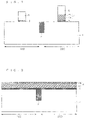
- a semiconductor substrate 1 which has an n-FET formation region 100 and a p-FET formation region 200 .
- the n-FET formation region 100 and the p-FET formation region 200 are electrically isolated by an element isolation film (STI film) 2 .
- STI film element isolation film
- well regions of given conductivity types and active regions of given conductivity types are formed in the semiconductor substrate 1 .
- a gate insulating film 3 having a high dielectric constant (High-k) is formed on the semiconductor substrate 1 .
- the gate insulating film 3 can be formed by CVD (Chemical Vapor Deposition), for example.
- the high-dielectric-constant gate insulating film 3 may be formed of HfSiON (dielectric constant: 10 to 15), HfO 2 (dielectric constant: around 24), or La 2 O 3 (dielectric constant: around 27).
- a metal film 4 is formed on the gate insulating film 3 , for the purpose of forming a gate electrode.
- the metal film 4 can be formed by CVD, for example.
- the metal film 4 may be a film of metal other than Al.
- the metal film 4 may be a single-layer film of TiN, Ru, RuO, TaN, HfN, Ni, Re, Ir, Pt, or WN, or a stacked film including TiN and Ti films stacked in this order, or a stacked film including WN and WSi films stacked in this order.
- a resist 5 is formed in a given shape on the metal film 4 .
- the resist 5 is used as a mask in a wet etching process performed later. Accordingly, the resist 5 is formed in a given shape such that unwanted portions of the metal film 4 can be removed (in this example, the portion of the metal film 4 that resides in the n-FET region 100 is removed).
- the portion of the metal film 4 (the portion of the metal film 4 that resides in the n-FET formation region 100 ) is etched away (removed). In other words, the metal film 4 is left only in the p-FET formation region 200 .
- wet etching leaves less etching residues of the metal film 4 . Accordingly, it is not essential to perform a cleaning process for removing etching residues.
- the desirable conditions are: higher selectivity with respect to the resist; no damage (or less damage) to the high-dielectric-constant gate insulating film 3 ; and a higher etch rate to the metal film 4 .
- Chemical liquids that satisfy these conditions are liquids that at least contain acid. Accordingly, it is more desirable to use, as the given chemical liquid, hydrogen peroxide solution, mixed acid (mixed liquid of acids of two or more kinds, such as a mixed liquid of phosphoric acid, nitric acid, acetic acid, and water), hydrogen peroxide solution+ aqueous ammonia, or hydrogen peroxide solution+ mixed acid, for example.
- suitable temperatures for the given chemical liquids are from 23° C. to 80° C.
- the wet etching process is conducted in an apparatus of dip type, spray type, or single wafer processing type, for example.
- the resist 5 is removed and a polysilicon film 6 is formed over the semiconductor substrate 1 to cover the gate insulating film 3 and the metal film 4 . Subsequently, the polysilicon film 6 , the metal film 4 , and the gate insulating film 3 are patterned into a given shape.
- the gate insulating film 3 and the polysilicon film 6 stacked in this order in the n-FET formation region 100 form a gate structure on the semiconductor substrate 1 .
- the gate insulating film 3 , the metal film 4 , and the polysilicon film 6 stacked in this order form a gate structure on the semiconductor substrate.
- the gate electrode is made only of the polysilicon film 6
- the gate electrode in the p-FET formation region 200 is made of the metal film 4 and the polysilicon film 6 .
- wet etching is applied to the n-FET formation region 100 during the formation of the metal film 4 .
- wet etching does not involve generation of plasma. That is, adopting wet etching reduces the damage to the high-dielectric-constant gate insulating film 3 lying under the metal film 4 to be etched (removed).
- the thickness reduction of the gate insulating film 3 in the n-FET formation region 100 is suppressed. This prevents variation and increase of leakage current in the n-FET.
- the process of wet etching itself causes less thickness reduction of the gate insulating film 3 . Also, unlike dry etching, wet etching causes almost no etching residue of the metal film 4 . Accordingly, adopting the manufacturing method of this preferred embodiment removes the need for a cleaning process for removing etching residues.
- the inventors and others made metal films on high-dielectric-constant insulating films and applied wet etching to the metal films to verify the effects of the invention.
- the high-dielectric-constant insulating films were made of HfSiON, with film thicknesses of 1 nm to 5 mm.
- the high-dielectric-constant insulating films were annealed at about 1000° C. for stabilization.
- the metal films were made of TiN, with thicknesses of 5 nm or more.
- the temperature of the chemical was 65° C.
- the TiN (metal film) was etched about 8.5 nm in five minutes on average.
- the amount of etch increased as the etching time was increased, and the film was etched about 27.3 nm in 20 minutes on average.
- the HfSiON high-dielectric-constant insulating film
- the wet etching unlike dry etching, does not require generation of plasma, and it therefore causes almost no damage (i.e., almost no deterioration of the bonding of molecules) to the HfSiON (high-dielectric-constant insulating film). Accordingly, the thickness of the HfSiON (high-dielectric-constant insulating film) is not reduced even when a cleaning process or the like is applied after the wet etching (this was also experimentally verified).
- wet etching causes almost no etching residues, and therefore the cleaning process may be omitted.
- the metal film 4 of the example is formed as a single-layer film, but it may be formed as a stacked film including a TiN film (or a WN film) 4 a and a Ti film (or a WSi film) 4 b stacked in this order (see FIG. 7 ). As shown in FIG. 7 , placing the Ti film (or WSi film) 4 b between the TiN film (or WN film) 4 a and the polysilicon film 6 reduces the interface resistance between the TiN film (or WN film) 4 a and the polysilicon film 6 .
- the metal film 4 is formed as a stacked film including the TiN film 4 a and the Ti film 4 b stacked in this order, the stacked film can be removed by wet etching using a hydrogen peroxide solution, for example.
- the metal film 4 is a stacked film including a WN film 4 a and a WSi film 4 b stacked in this order
- the stacked film can be removed by wet etching using a mixture of aqueous ammonia and hydrogen peroxide solution, for example (removal of the metal film 4 with one kind of chemical liquid).
- the WSi film 4 b may be removed by wet etching using a mixture of aqueous ammonia and hydrogen peroxide solution
- the WN film 4 a may be removed by wet etching using a hydrogen peroxide solution or mixed acid (for example, a mixture of phosphoric acid, nitric acid, acetic acid and water) (removal of the metal film 4 with two kinds of chemical liquids).
- the gate electrode in the n-FET formation region 100 is formed only of the polysilicon film 6
- the gate electrode in the p-FET formation region 200 is formed of the TiN film (or WN film) 4 a , the Ti film (or WSi film) 4 b , and the polysilicon film 6 .
- the first preferred embodiment has shown an example in which the metal film 4 is formed as a stacked film including a TiN film 4 a and a Ti film 4 b stacked in this order (see FIG. 7 ). Now, a method of manufacturing a semiconductor device will be described in which the stacked film of TiN film 4 a and Ti film 4 b is adopted as the metal film 4 .
- the metal film 4 shown in FIG. 3 is the TiN film 4 a.
- the Ti film 4 b is formed on the TiN film 4 a so that the Ti film 4 b can form a gate electrode together with the TiN film 4 a .
- the Ti film 4 b can be formed by CVD, for example.
- a resist 10 is formed in a given shape on the Ti film 4 b .
- the resist 10 is used as a mask in a wet etching process performed later. Accordingly, the resist 10 is formed in a given shape such that unwanted portions of the TiN film 4 a and the Ti film 4 b can be removed (in this preferred embodiment, the portion of the TiN film 4 a and the Ti film 4 b that resides in the n-FET region 100 is removed).
- the wet etching to the metal film 4 including the TiN film 4 a and the Ti film 4 b is carried out as described in the first preferred embodiment. In this case, it is possible to remove the TiN film 4 a and the Ti film 4 b from the n-FET formation region 100 without reducing the thickness of the gate insulating film 3 .
- FIG. 11 shows experimental results about a relation between the temperature of the chemical liquid (hydrogen peroxide solution) used for the wet etching and the etch rates to the TiN film 4 a and the Ti film 4 b that the chemical liquid exhibited.
- the horizontal axis shows the temperature (° C.) of the hydrogen peroxide solution.
- the vertical axis shows the etch rates ( ⁇ /min).
- the square marks show data about the TiN film 4 a
- the circular marks show data about the Ti film 4 b.
- the etch rate to the Ti film 4 b is smaller than the etch rate to the TiN film 4 a when the wet etching is conducted with a hydrogen peroxide solution at temperatures of 50° C. or higher.
- the wet etching for removing the TiN film 4 a and the Ti film 4 b uses a hydrogen peroxide solution as the given chemical liquid at a temperature of 50° C. or higher.
- the wet etching using the given chemical liquid etches away (removes) part of the TiN film 4 a and part of the Ti film 4 b (the part of the TiN film 4 a and the Ti film 4 b that is formed in the n-FET formation region 100 ) without causing horizontal over-etch of the Ti film 4 b in the p-FET formation region 200 (hereinafter, this condition is referred to as “desirably shaped”).
- this condition is referred to as “desirably shaped”.
- the gate insulating film 3 in the n-FET formation region 100 is not damaged because wet etching is adopted. Also, almost no etching residue is left.
- the resist 10 is removed, and the polysilicon film 6 is formed over the semiconductor substrate 1 to cover the gate insulating film 3 and the metal film 4 . Subsequently, the polysilicon film 6 , the metal film 4 , and the gate insulating film 3 are patterned into a given shape.
- a stacked film including the TiN film 4 a and the Ti film 4 b stacked in this order is adopted as the metal film 4 . Accordingly, when the polysilicon film 6 is formed on the Ti film 4 b , the contact resistance between the TiN film 4 a and the polysilicon film 6 is reduced.
- the wet etching to the stacked metal film 4 uses a hydrogen peroxide solution as the given chemical liquid at a temperature of 50° C. or higher. This allows the metal film 4 to be left only in the p-FET formation region 200 , with the Ti film 4 b shaped desirably. Also, adopting wet etching keeps the gate insulating film 3 undamaged in the n-FET formation region 100 , as described in the first preferred embodiment. Furthermore, almost no etching residue is left.
- the semiconductor device manufacturing method of this preferred embodiment relates to the process from the structure shown in FIG. 5 to the structure shown in FIG. 6 of the first preferred embodiment.
- the resist 5 is removed from the structure of FIG. 5 , and the polysilicon film 6 is formed over the semiconductor substrate 1 to cover the metal film 4 and the gate insulating film 3 (see FIG. 13 ). Then, a resist 25 is formed in a given shape on the polysilicon film 6 (see FIG. 13 ).
- the polysilicon film 6 , the metal film 4 , and the gate insulating film 3 are etched by using the resist 25 as a mask. Suppose that this etching is done only by dry etching.
- the upper surface of the polysilicon film 6 has a difference in level between the n-FET formation region 100 and the p-FET formation region 200 . Accordingly, when the dry etching to the polysilicon film 6 finishes, dry etching to the gate insulating film 3 starts in the n-FET formation region 100 , while dry etching to the metal film 4 and the gate insulating film 3 starts in the p-FET formation region 200 .
- the semiconductor substrate 1 is exposed by the time when the dry etching to the gate insulating film 3 in the p-FET formation region 200 ends. That is, the portion in the vicinity of the upper surface of the semiconductor substrate 1 in the n-FET formation region 100 is damaged by the dry etching for a longer period of time. The damage to the semiconductor substrate 1 deteriorates performance of the completed transistors.
- the following procedure is carried out during the formation of gate structures.
- a dry etching process is performed using the resist 25 as a mask. Then, as shown in FIG. 14 , this dry etching is ended when the metal film 4 is exposed (reached) in the p-FET formation region 200 .
- the timing for ending the dry etching can be determined by using end point techniques, for example.
- FIG. 15 shows the structure obtained after the wet etching of the metal film 4 .
- This wet etching process is conducted using any of the given chemical liquids explained in the first preferred embodiment. As described in the first preferred embodiment, wet etching using the given chemical liquids hardly etches the gate insulating film 3 .
- the gate insulating film 3 is removed in the n-FET formation region 100 and the p-FET formation region 200 , using the resist 25 as a mask.
- the gate insulating film 3 can be removed by wet etching, for example.
- FIG. 16 shows the structure obtained after the removal of the gate insulating film 3 .
- the structure of FIG. 6 is obtained by removing the resist 25 .
- the gate insulating film 3 is removed by dry etching, the upper surface of the semiconductor substrate 1 is damaged. It is therefore preferable to remove the gate insulating film 3 by wet etching.
- dry etching is applied to the polysilicon film 6 and wet etching is applied to the metal film 4 .
- the semiconductor device manufacturing method of this preferred embodiment is applicable also to structures in which the metal film 4 is a stacked film including a TiN film and a Ti film stacked in this order, or a stacked film including a WN film and a WSi film stacked in this order, for example.
- a stacked film including a TiN film and a Ti film stacked in this order is adopted as the metal film 4 .
- a stacked film including a WN film and a WSi film stacked in this order i.e., a stacked film in which a first metal film and a second metal film that at least contains silicon are stacked in this order
- a dry etching is applied to the polysilicon film 6 and the WSi film (second metal film). The dry etching is stopped at the time when the dry etching reaches the WN film (first metal film). This dry etching removes part of the polysilicon film 6 and part of the WSi film (second metal film). Next, a wet etching is performed to remove part of the WN film (first metal film).
- the polysilicon film forming the gate electrode in the n-FET formation region 100 is shaved (thinned) in horizontal direction. That is, because the given chemical liquid is selected to remove the silicon-containing film, the chemical liquid also wet-etches the polysilicon in horizontal direction.
- the horizontal thinning of the polysilicon film 6 forming the gate electrode is avoided by adopting the process of dry-etching such WSi film (second metal film) et al. and wet-etching only the WN film (first metal film).
- the preferred embodiments described above adopt high-dielectric-constant material for the gate insulating film 3 , considering miniaturization of the semiconductor device.
- the material of the gate insulating film 3 is not restricted by this example, but the present invention is effective also in methods of manufacturing semiconductor devices in which the gate insulating film 3 is made of material having a low dielectric constant.
- the preferred embodiments have described an application of the present invention to a method of manufacturing a semiconductor device having the n-FET formation region 100 and the p-FET formation region 200 .
- the present invention is applicable to methods of manufacturing any semiconductor devices in which a metal film for a gate electrode is formed on a gate insulating film.
Abstract
Description
Claims (3)
Applications Claiming Priority (2)
| Application Number | Priority Date | Filing Date | Title |
|---|---|---|---|
| JP2005313635A JP2007123548A (en) | 2005-10-28 | 2005-10-28 | Manufacturing method for semiconductor device |
| JP2005-313635 | 2005-10-28 |
Publications (2)
| Publication Number | Publication Date |
|---|---|
| US20070099406A1 US20070099406A1 (en) | 2007-05-03 |
| US7537987B2 true US7537987B2 (en) | 2009-05-26 |
Family
ID=37996965
Family Applications (1)
| Application Number | Title | Priority Date | Filing Date |
|---|---|---|---|
| US11/551,861 Expired - Fee Related US7537987B2 (en) | 2005-10-28 | 2006-10-23 | Semiconductor device manufacturing method |
Country Status (3)
| Country | Link |
|---|---|
| US (1) | US7537987B2 (en) |
| JP (1) | JP2007123548A (en) |
| CN (1) | CN1956152A (en) |
Families Citing this family (6)
| Publication number | Priority date | Publication date | Assignee | Title |
|---|---|---|---|---|
| JP2009044051A (en) * | 2007-08-10 | 2009-02-26 | Panasonic Corp | Semiconductor device and its manufacturing method |
| JP2009295926A (en) * | 2008-06-09 | 2009-12-17 | Panasonic Corp | Semiconductor device |
| US7790624B2 (en) * | 2008-07-16 | 2010-09-07 | Global Foundries Inc. | Methods for removing a metal-comprising material from a semiconductor substrate |
| TWI371085B (en) * | 2008-08-12 | 2012-08-21 | Vanguard Int Semiconduct Corp | Fabrication methods for integration cmos and bjt devices |
| JP2011009329A (en) * | 2009-06-24 | 2011-01-13 | Panasonic Corp | Semiconductor device and method of manufacturing the same |
| CN104538308A (en) * | 2014-12-25 | 2015-04-22 | 上海芯亮电子科技有限公司 | Method for reducing on resistance of power transistor |
Citations (8)
| Publication number | Priority date | Publication date | Assignee | Title |
|---|---|---|---|---|
| US5258095A (en) * | 1989-01-20 | 1993-11-02 | Fujitsu Limited | Method for producing a device having an insulator sandwiched between two semiconductor layers |
| US6531728B2 (en) * | 1999-09-02 | 2003-03-11 | Micron Technology, Inc. | Oxide etching method and structures resulting from same |
| WO2004095572A1 (en) | 2003-04-22 | 2004-11-04 | National University Of Singapore | A method of fabricating a cmos device with dual metal gate electrodes |
| US20040266077A1 (en) * | 2003-06-27 | 2004-12-30 | Yee-Chia Yeo | Structure and method for forming the gate electrode in a multiple-gate transistor |
| JP2005072316A (en) | 2003-08-26 | 2005-03-17 | Toshiba Corp | Method for manufacturing semiconductor device |
| US20070152276A1 (en) * | 2005-12-30 | 2007-07-05 | International Business Machines Corporation | High performance CMOS circuits, and methods for fabricating the same |
| US20070228458A1 (en) * | 2006-03-29 | 2007-10-04 | International Business Machines Corporation | Dual metal integration scheme based on full silicidation of the gate electrode |
| US20070284670A1 (en) * | 2006-04-20 | 2007-12-13 | Kazuhiko Yamamoto | Semiconductor device and fabrication method therefor |
Family Cites Families (6)
| Publication number | Priority date | Publication date | Assignee | Title |
|---|---|---|---|---|
| US6444512B1 (en) * | 2000-06-12 | 2002-09-03 | Motorola, Inc. | Dual metal gate transistors for CMOS process |
| KR100422342B1 (en) * | 2000-12-29 | 2004-03-10 | 주식회사 하이닉스반도체 | Method for manufacturing gate in semiconductor device |
| US6518106B2 (en) * | 2001-05-26 | 2003-02-11 | Motorola, Inc. | Semiconductor device and a method therefor |
| US6790719B1 (en) * | 2003-04-09 | 2004-09-14 | Freescale Semiconductor, Inc. | Process for forming dual metal gate structures |
| BE1015723A4 (en) * | 2003-10-17 | 2005-07-05 | Imec Inter Uni Micro Electr | METHOD FOR MANUFACTURING OF SEMICONDUCTOR DEVICES WITH silicided electrodes. |
| JP2005142539A (en) * | 2003-10-17 | 2005-06-02 | Toshiba Corp | Semiconductor device and manufacturing method therefor |
-
2005
- 2005-10-28 JP JP2005313635A patent/JP2007123548A/en active Pending
-
2006
- 2006-10-23 US US11/551,861 patent/US7537987B2/en not_active Expired - Fee Related
- 2006-10-27 CN CNA2006101436583A patent/CN1956152A/en active Pending
Patent Citations (9)
| Publication number | Priority date | Publication date | Assignee | Title |
|---|---|---|---|---|
| US5258095A (en) * | 1989-01-20 | 1993-11-02 | Fujitsu Limited | Method for producing a device having an insulator sandwiched between two semiconductor layers |
| US6531728B2 (en) * | 1999-09-02 | 2003-03-11 | Micron Technology, Inc. | Oxide etching method and structures resulting from same |
| WO2004095572A1 (en) | 2003-04-22 | 2004-11-04 | National University Of Singapore | A method of fabricating a cmos device with dual metal gate electrodes |
| US20040266077A1 (en) * | 2003-06-27 | 2004-12-30 | Yee-Chia Yeo | Structure and method for forming the gate electrode in a multiple-gate transistor |
| US20060091428A1 (en) * | 2003-06-27 | 2006-05-04 | Yee-Chia Yeo | Structure and method for forming the gate electrode in a multiple-gate transistor |
| JP2005072316A (en) | 2003-08-26 | 2005-03-17 | Toshiba Corp | Method for manufacturing semiconductor device |
| US20070152276A1 (en) * | 2005-12-30 | 2007-07-05 | International Business Machines Corporation | High performance CMOS circuits, and methods for fabricating the same |
| US20070228458A1 (en) * | 2006-03-29 | 2007-10-04 | International Business Machines Corporation | Dual metal integration scheme based on full silicidation of the gate electrode |
| US20070284670A1 (en) * | 2006-04-20 | 2007-12-13 | Kazuhiko Yamamoto | Semiconductor device and fabrication method therefor |
Also Published As
| Publication number | Publication date |
|---|---|
| US20070099406A1 (en) | 2007-05-03 |
| CN1956152A (en) | 2007-05-02 |
| JP2007123548A (en) | 2007-05-17 |
Similar Documents
| Publication | Publication Date | Title |
|---|---|---|
| US7402530B2 (en) | Method for manufacturing semiconductor device and semiconductor device | |
| JP4282616B2 (en) | Manufacturing method of semiconductor device | |
| CN109216198B (en) | Gate stack structure and forming method thereof | |
| TWI658514B (en) | Method of manufacturing transistor | |
| US11101178B2 (en) | Semiconductor integrated circuit | |
| US7537987B2 (en) | Semiconductor device manufacturing method | |
| JP4409028B2 (en) | Semiconductor device formation method | |
| KR100769415B1 (en) | Method of fabricating semiconductor device | |
| US8119537B2 (en) | Selective etching of oxides to metal nitrides and metal oxides | |
| US8314022B1 (en) | Method for etching gate stack | |
| US7785957B2 (en) | Post metal gate VT adjust etch clean | |
| US20150137197A1 (en) | Semiconductor structure having trimming spacers | |
| CN109427670B (en) | Wrap-around epitaxial structure and method | |
| JP2007036116A (en) | Semiconductor device manufacturing method | |
| KR100663357B1 (en) | Methods of forming a transistor having a metal nitride layer pattern | |
| US20020146911A1 (en) | Semiconductor device and method of manufacturing the same | |
| US8546016B2 (en) | Solutions for cleaning semiconductor structures and related methods | |
| CN108807377B (en) | Semiconductor device and method of forming the same | |
| US20070082493A1 (en) | Method of manufacturing semiconductor device | |
| CN105990234B (en) | The forming method of semiconductor devices | |
| JP4082280B2 (en) | Semiconductor device and manufacturing method thereof | |
| US20060166379A1 (en) | Method for manufacturing ferroelectric capacitor | |
| US9394509B2 (en) | Cleaning solution composition and method of cleaning semiconductor device using the same | |
| JP2009170729A (en) | Method of manufacturing semiconductor device | |
| JP2008135765A (en) | Semiconductor device |
Legal Events
| Date | Code | Title | Description |
|---|---|---|---|
| AS | Assignment |
Owner name: RENESAS TECHNOLOGY CORP., JAPAN Free format text: ASSIGNMENT OF ASSIGNORS INTEREST;ASSIGNORS:HIGASHI, MASAHIKO;KUME, SATOSHI;YUGAMI, JIRO;AND OTHERS;REEL/FRAME:018680/0476 Effective date: 20061016 |
|
| STCF | Information on status: patent grant |
Free format text: PATENTED CASE |
|
| FEPP | Fee payment procedure |
Free format text: PAYOR NUMBER ASSIGNED (ORIGINAL EVENT CODE: ASPN); ENTITY STATUS OF PATENT OWNER: LARGE ENTITY |
|
| AS | Assignment |
Owner name: RENESAS ELECTRONICS CORPORATION, JAPAN Free format text: CHANGE OF NAME;ASSIGNOR:NEC ELECTRONICS CORPORATION;REEL/FRAME:024915/0526 Effective date: 20100401 Owner name: NEC ELECTRONICS CORPORATION, JAPAN Free format text: MERGER;ASSIGNOR:RENESAS TECHNOLOGY CORP.;REEL/FRAME:024915/0556 Effective date: 20100401 |
|
| FPAY | Fee payment |
Year of fee payment: 4 |
|
| FPAY | Fee payment |
Year of fee payment: 8 |
|
| AS | Assignment |
Owner name: RENESAS ELECTRONICS CORPORATION, JAPAN Free format text: CHANGE OF ADDRESS;ASSIGNOR:RENESAS ELECTRONICS CORPORATION;REEL/FRAME:044928/0001 Effective date: 20150806 |
|
| FEPP | Fee payment procedure |
Free format text: MAINTENANCE FEE REMINDER MAILED (ORIGINAL EVENT CODE: REM.); ENTITY STATUS OF PATENT OWNER: LARGE ENTITY |
|
| LAPS | Lapse for failure to pay maintenance fees |
Free format text: PATENT EXPIRED FOR FAILURE TO PAY MAINTENANCE FEES (ORIGINAL EVENT CODE: EXP.); ENTITY STATUS OF PATENT OWNER: LARGE ENTITY |
|
| STCH | Information on status: patent discontinuation |
Free format text: PATENT EXPIRED DUE TO NONPAYMENT OF MAINTENANCE FEES UNDER 37 CFR 1.362 |
|
| FP | Lapsed due to failure to pay maintenance fee |
Effective date: 20210526 |