US7515224B2 - Display substrate, method of manufacturing the same and display device having the same - Google Patents
Display substrate, method of manufacturing the same and display device having the same Download PDFInfo
- Publication number
- US7515224B2 US7515224B2 US11/504,504 US50450406A US7515224B2 US 7515224 B2 US7515224 B2 US 7515224B2 US 50450406 A US50450406 A US 50450406A US 7515224 B2 US7515224 B2 US 7515224B2
- Authority
- US
- United States
- Prior art keywords
- layer
- insulation layer
- organic insulation
- electrode
- gate
- Prior art date
- Legal status (The legal status is an assumption and is not a legal conclusion. Google has not performed a legal analysis and makes no representation as to the accuracy of the status listed.)
- Expired - Fee Related, expires
Links
Images


Classifications
-
- G—PHYSICS
- G02—OPTICS
- G02F—OPTICAL DEVICES OR ARRANGEMENTS FOR THE CONTROL OF LIGHT BY MODIFICATION OF THE OPTICAL PROPERTIES OF THE MEDIA OF THE ELEMENTS INVOLVED THEREIN; NON-LINEAR OPTICS; FREQUENCY-CHANGING OF LIGHT; OPTICAL LOGIC ELEMENTS; OPTICAL ANALOGUE/DIGITAL CONVERTERS
- G02F1/00—Devices or arrangements for the control of the intensity, colour, phase, polarisation or direction of light arriving from an independent light source, e.g. switching, gating or modulating; Non-linear optics
- G02F1/01—Devices or arrangements for the control of the intensity, colour, phase, polarisation or direction of light arriving from an independent light source, e.g. switching, gating or modulating; Non-linear optics for the control of the intensity, phase, polarisation or colour
- G02F1/13—Devices or arrangements for the control of the intensity, colour, phase, polarisation or direction of light arriving from an independent light source, e.g. switching, gating or modulating; Non-linear optics for the control of the intensity, phase, polarisation or colour based on liquid crystals, e.g. single liquid crystal display cells
- G02F1/133—Constructional arrangements; Operation of liquid crystal cells; Circuit arrangements
- G02F1/1333—Constructional arrangements; Manufacturing methods
- G02F1/1335—Structural association of cells with optical devices, e.g. polarisers or reflectors
- G02F1/133553—Reflecting elements
- G02F1/133555—Transflectors
-
- G—PHYSICS
- G02—OPTICS
- G02F—OPTICAL DEVICES OR ARRANGEMENTS FOR THE CONTROL OF LIGHT BY MODIFICATION OF THE OPTICAL PROPERTIES OF THE MEDIA OF THE ELEMENTS INVOLVED THEREIN; NON-LINEAR OPTICS; FREQUENCY-CHANGING OF LIGHT; OPTICAL LOGIC ELEMENTS; OPTICAL ANALOGUE/DIGITAL CONVERTERS
- G02F1/00—Devices or arrangements for the control of the intensity, colour, phase, polarisation or direction of light arriving from an independent light source, e.g. switching, gating or modulating; Non-linear optics
- G02F1/01—Devices or arrangements for the control of the intensity, colour, phase, polarisation or direction of light arriving from an independent light source, e.g. switching, gating or modulating; Non-linear optics for the control of the intensity, phase, polarisation or colour
- G02F1/13—Devices or arrangements for the control of the intensity, colour, phase, polarisation or direction of light arriving from an independent light source, e.g. switching, gating or modulating; Non-linear optics for the control of the intensity, phase, polarisation or colour based on liquid crystals, e.g. single liquid crystal display cells
- G02F1/133—Constructional arrangements; Operation of liquid crystal cells; Circuit arrangements
- G02F1/1333—Constructional arrangements; Manufacturing methods
- G02F1/1335—Structural association of cells with optical devices, e.g. polarisers or reflectors
- G02F1/133526—Lenses, e.g. microlenses or Fresnel lenses
-
- G—PHYSICS
- G02—OPTICS
- G02F—OPTICAL DEVICES OR ARRANGEMENTS FOR THE CONTROL OF LIGHT BY MODIFICATION OF THE OPTICAL PROPERTIES OF THE MEDIA OF THE ELEMENTS INVOLVED THEREIN; NON-LINEAR OPTICS; FREQUENCY-CHANGING OF LIGHT; OPTICAL LOGIC ELEMENTS; OPTICAL ANALOGUE/DIGITAL CONVERTERS
- G02F1/00—Devices or arrangements for the control of the intensity, colour, phase, polarisation or direction of light arriving from an independent light source, e.g. switching, gating or modulating; Non-linear optics
- G02F1/01—Devices or arrangements for the control of the intensity, colour, phase, polarisation or direction of light arriving from an independent light source, e.g. switching, gating or modulating; Non-linear optics for the control of the intensity, phase, polarisation or colour
- G02F1/13—Devices or arrangements for the control of the intensity, colour, phase, polarisation or direction of light arriving from an independent light source, e.g. switching, gating or modulating; Non-linear optics for the control of the intensity, phase, polarisation or colour based on liquid crystals, e.g. single liquid crystal display cells
- G02F1/133—Constructional arrangements; Operation of liquid crystal cells; Circuit arrangements
- G02F1/1333—Constructional arrangements; Manufacturing methods
- G02F1/1335—Structural association of cells with optical devices, e.g. polarisers or reflectors
- G02F1/13356—Structural association of cells with optical devices, e.g. polarisers or reflectors characterised by the placement of the optical elements
- G02F1/133565—Structural association of cells with optical devices, e.g. polarisers or reflectors characterised by the placement of the optical elements inside the LC elements, i.e. between the cell substrates
Definitions
- Exemplary embodiments of the present invention relate to a display substrate, a method of manufacturing the display substrate and a display device having the display substrate. More particularly, exemplary embodiments of the present invention relate to a display substrate having an improved display quality, a method of manufacturing the display substrate and a display device having the display substrate.
- liquid crystal display device is widely employed in the industry because the liquid crystal display device is relatively thin and light rather than the other kinds of display devices. Also, the liquid crystal display device has been applied in a more expanded field because manufacturing the liquid crystal display device is relatively easy.
- the liquid crystal display device is classified into a transmissive liquid crystal display device, a reflective liquid crystal display device and a transflective liquid crystal display device.
- the transmissive liquid crystal display device displays images using a light provided from a backlight assembly positioned at a rear side of a liquid crystal display panel.
- the reflective liquid crystal display device displays images using an external light provided from outside.
- the transflective liquid crystal apparatus operates in a transmissive display mode displaying images using a light provided from the backlight assembly where there is no external light source such as indoor environment.
- the transflective liquid crystal apparatus operates in a reflective display mode displaying images using a reflected light where there is external light source such as an outdoor environment.
- a microlens pattern is formed to increase a reflexibility of a natural light and to improve a visual angle.
- the microlens pattern is formed by performing a deposition process of a photosensitive organic layer, and by performing an exposure process and a development process.
- the photosensitive organic layer deposited by a spin coating generates an undesirable effect such as a thickness variation between a central portion and an edge portion of a glass substrate.
- a crosslinking process such as the exposure process of the photosensitive organic layer, the development process of the photosensitive organic layer, etc., is performed, the microlens pattern may be deformed.
- Exemplary embodiments provide a display substrate precisely controlling a microlens pattern to improve a reflexibility of a light.
- Exemplary embodiments provide a method of manufacturing the above-mentioned display substrate.
- Exemplary embodiments provide a display device having the above-mentioned display substrate.
- An exemplary embodiment provides a display substrate.
- the display substrate includes a transparent substrate, a pixel layer, an organic insulation layer, a transparent electrode and a reflective electrode.
- the pixel layer is formed on the transparent substrate and the pixel layer includes pixel parts having a matrix shape.
- the organic insulation layer is formed on the pixel layer and includes a microlens pattern having a depth of no less than about 1.5 micrometers ( ⁇ m) formed on an upper portion of the organic insulation layer.
- the transparent electrode is formed on the organic insulation layer.
- the reflective electrode is partially formed on the transparent electrode to define a reflective region and a transmissive region.
- An exemplary embodiment provides a method of manufacturing a display substrate.
- a pixel layer including pixel parts having a matrix shape is formed on a transparent substrate.
- An organic insulation layer including a microlens pattern having a depth of no less than about 1.5 ⁇ m, is formed on the pixel layer.
- a transparent electrode is formed on the organic insulation layer.
- a reflective electrode to define a reflective region and a transmissive region is formed on the transparent electrode.
- the organic insulation layer may be formed by using an organic insulation layer sheet.
- An exemplary embodiment provides a display device.
- the display device includes a display substrate, an opposite substrate and a liquid crystal layer.
- the display substrate includes an organic insulation layer, a transparent electrode and a reflective electrode.
- the organic insulation layer includes a microlens pattern having a depth of no less than about 1.5 ⁇ m.
- the transparent electrode is formed on the organic insulation layer.
- the reflective electrode is partially formed on the transparent electrode to define a reflective region and a transmissive region.
- the opposite substrate faces the display substrate.
- the liquid crystal layer is disposed between the display substrate and the opposite substrate.
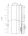
- FIG. 1 is a plan view illustrating an exemplary embodiment of a display substrate in accordance with the present invention
- FIG. 2 is a cross-sectional view illustrating the display device taken along line I-I′ in FIG. 1 ;
- FIG. 3 is an enlarged cross-sectional view illustrating portion “A” in FIG. 2 ;
- FIG. 4 is a simulation graph illustrating an exemplary embodiment of a reflexibility of a light according to a depth A 1 of a microlens pattern 232 using an apparatus measuring an integrating sphere reflexibility;
- FIG. 5 is a cross-sectional view illustrating an exemplary embodiment of an organic insulation layer sheet to form an organic insulation layer in FIG. 2 ;
- FIGS. 6 to 10 are cross-sectional views illustrating an exemplary embodiment of a method of manufacturing a display substrate in accordance with the present invention.
- first, second, third etc. may be used herein to describe various elements, components, regions, layers and/or sections, these elements, components, regions, layers and/or sections should not be limited by these terms. These terms are only used to distinguish one element, component, region, layer or section from another region, layer or section. Thus, a first element, component, region, layer or section discussed below could be termed a second element, component, region, layer or section without departing from the teachings of the present invention.
- spatially relative terms such as “lower,” “upper” and the like, may be used herein for ease of description to describe one element or feature's relationship to another element(s) or feature(s) as illustrated in the figures. It will be understood that the spatially relative terms are intended to encompass different orientations of the device in use or operation in addition to the orientation depicted in the figures. For example, if the device in the figures is turned over, elements described as “lower” relative to other elements or features would then be oriented “upper” relative to the other elements or features. Thus, the example term “lower” can encompass both an orientation of above and below. The device may be otherwise oriented (rotated 90 degrees or at other orientations) and the spatially relative descriptors used herein interpreted accordingly.
- Example embodiments of the present invention are described herein with reference to cross-section illustrations that are schematic illustrations of idealized embodiments (and intermediate structures) of the present invention. As such, variations from the shapes of the illustrations as a result, for example, of manufacturing techniques and/or tolerances, are to be expected. Thus, example embodiments of the present invention should not be construed as limited to the particular shapes of regions illustrated herein but are to include deviations in shapes that result, for example, from manufacturing. The regions illustrated in the figures are schematic in nature and their shapes are not intended to illustrate the actual shape of a region of a device and are not intended to limit the scope of the present invention.
- FIG. 1 is a plan view illustrating an exemplary embodiment of a display substrate of the present invention.
- FIG. 2 is a cross-sectional view illustrating the display device taken along line I-I′ in FIG. 1 .
- a display device 100 includes a display substrate 200 , a opposite substrate 300 facing the display substrate 200 and a liquid crystal layer 400 disposed between the display substrate 200 and the opposite substrate 300 .
- the display substrate 200 includes a reflection region RR and a transmissive region TR.
- a reflection region RR a natural light incident from an upper side of the display device 100 is reflected.
- a transmissive region TR a backlight incident from a lower side of the display device 100 is transmitted.
- the display substrate 200 includes a transparent substrate 210 , a pixel layer 220 , an organic insulation layer 230 , a transparent electrode 240 and a reflective electrode 250 .
- the transparent substrate 210 may include a transparent material transmitting a light.
- the transparent substrate 210 includes glass.
- the pixel layer 220 is formed on the transparent substrate 210 .
- the pixel layer 220 includes pixel parts 221 arranged on the transparent substrate 210 in substantially a matrix shape.
- the pixel layer 220 includes gate lines 222 , a gate insulation layer 223 , data lines 224 , a thin-film transistor 225 and a passivation layer 226 .
- the gate lines 222 are formed on the transparent substrate 210 to define an upper side and a lower side of the pixel part 221 in FIG. 1 .
- the gate insulation layer 223 is formed on the transparent substrate 210 to cover the gate lines 222 .
- the gate insulation layer 223 includes a silicon nitride layer or a silicon oxide layer.
- the data lines 224 are formed on the gate insulation layer 223 to define a left side and a right side of the pixel part 221 in FIG. 2 .
- the thin-film transistor 225 is connected to the gate lines 222 and the data lines 224 , and is formed in the pixel part 221 .
- the thin-film transistor 225 applies an image signal to the transparent electrode 240 responding to a scan signal transmitted through the gate lines 222 .
- the thin-film transistor 225 includes a gate electrode G, an active layer 227 , a source electrode S and a drain electrode D.
- the gate electrode G is connected to the gate line 222 .
- the gate electrode G serves as a gate terminal of the thin-film transistor 225 .
- the active layer 227 is formed on the gate insulation layer 223 , corresponding in location and/or dimension to the gate electrode G.
- the active layer 227 includes a semiconductor layer 227 A and an ohmic contact layer 227 B.
- the semiconductor layer 227 A may include amorphous silicon.
- the ohmic contact layer 227 B may include amorphous silicon heavily doped with n-type impurities.
- the source electrode S is connected to the data line 224 .
- the source electrode S is formed to extend to an upper portion of the active layer 227 .
- the source electrode S serves as a source terminal of the thin-film transistor 225 .
- the drain electrode D is formed on the active layer 227 and spaced apart from the source electrode S.
- the drain electrode D serves as a drain terminal of the thin-film transistor 225 .
- the drain electrode D is connected to the transparent electrode 240 through a contact hole 228 .
- the contact hole 228 is formed through the passivation layer 226 and the organic insulation layer 230 .
- the source electrode S and the drain electrode D are disposed on the active layer 227 and spaced apart from each other.
- a channel layer of the thin-film transistor 225 is defined by a distance between the source electrode S and the drain electrode D.
- the passivation layer 226 is formed on the gate insulation layer 223 where the date lines 224 and the thin-film transistor 225 are formed.
- the passivation layer 226 covers the date lines 224 and the thin-film transistor 225 .
- the passivation layer 226 includes a silicon nitride layer or a silicon oxide layer.
- the organic insulation layer 230 is formed on the pixel layer 220 .
- the contact hole 228 for exposing the drain electrode D of the thin-film transistor 225 is formed through the organic insulation layer 230 and the passivation layer 226 .
- a microlens pattern 232 is formed on an upper portion of the organic insulation layer 230 to increase a reflexibility of a light reflected by the reflective electrode 250 and to improve a visual angle.
- FIG. 3 is an enlarged cross-sectional view illustrating portion “A” in FIG. 2 .
- the microlens pattern 232 includes microlenses 234 having substantially concave lens shapes.
- the microlenses 234 are arranged to be conformal with each other by a uniform interval.
- the microlenses 234 may have convex lens shapes.
- the reflexibility of a light incident from outside is affected by a depth A 1 of the microlens pattern 231 and a diameter A 2 of the microlens 234 .
- the reflexibility of a light incident from the outside is most affected by the depth A 1 of the microlens pattern 231 .
- FIG. 4 is a simulation graph illustrating an exemplary embodiment of a reflexibility of a light according to a depth A 1 of the microlens pattern 232 using an apparatus measuring an integrating sphere reflexibility.
- a point A indicates a depth of 0.8 micrometers ( ⁇ m) in the microlens pattern
- a point B indicates a depth of 1.1 ⁇ m
- a point C indicates a depth of 1.4 ⁇ m
- a point D indicates a depth of 1.8 ⁇ m
- a point E indicates a depth of 2.3 ⁇ m
- a point F indicates a depth of 2.8 ⁇ m
- a point G indicates a depth of 3.1 ⁇ m
- a point H indicates a depth of 3.5 ⁇ m.
- the reflexibility increases from the point A to the point F, and then the reflexibility abruptly decreases from the point F to the point H.
- the reflexibility increases from a depth of 0.8 ⁇ m at point A to a depth of 2.8 ⁇ m at point F.
- the reflexibility increases.
- the reflexibility decreases.
- the reflexibility is no less than about 80%.
- the depth A 1 of the microlens pattern 232 is formed in a range of about 1.5 ⁇ m to about 2.8 ⁇ m, the reflexibility of a natural light incident from outside may be improved.
- the transparent electrode 240 is formed on the organic insulation layer 230 .
- the transparent electrode 240 is formed on the organic insulation electrode 230 corresponding to each pixel part 221 .
- the transparent electrode 240 is electrically connected to the drain electrode D through the contact hole 228 that is formed through the organic insulation layer 230 and the passivation layer 226 .
- the transparent electrode 240 may include a transparent conductive material transmitting a light.
- the transparent electrode 240 includes indium zinc oxide (“IZO”) or indium tin oxide (“ITO”).
- the reflective electrode 250 is formed on the transparent electrode 240 .
- the reflective electrode 250 may include a conductive material having a high reflexibility of a light to reflect a light.
- the reflective electrode 250 includes a single reflective layer or a double reflective layer.
- the single reflective layer includes an aluminum niodium layer.
- the double reflective layer includes an aluminum niodium layer and a molybdenum tungsten layer.
- the reflective electrode 250 is partially formed on the transparent electrode 240 to define the reflection region RR and the transmissive region TR.
- the reflective region RR is a region where the reflective electrode 250 exists and the transmissive region TR is a region where the reflective electrode 250 is removed and the transparent electrode 240 is exposed.
- the transmissive region TR provides a light for displaying images by transmitting a backlight incident from a lower side of the display device.
- the reflective region RR is a region to provide a light for displaying images by reflecting a natural light incident from an upper side of the display device.
- the transparent electrode 240 and the reflective electrode 250 are substantially uniformly formed on the organic insulation layer 230 so that the transparent electrode 240 and the reflective electrode 250 have substantially the same surface construction or profile as that of the organic insulation layer 230 .
- the reflective electrode 250 has substantially the same depth as that of the microlens pattern 232 of the organic insulation layer 230 .
- he opposite substrate 300 includes a transparent substrate 310 , a color filter layer 320 and a common electrode 330 .
- the transparent substrate 310 may include a transparent material to transmit a light.
- the transparent substrate 310 includes glass.
- the color filter layer 320 is formed on a surface of the transparent substrate 310 facing the display substrate 200 .
- the color filter layer 320 may include color pixels such as red, green, blue, etc. to realize color.
- the color filter layer 320 may be formed on the display substrate 200 .
- the common electrode 330 is formed on the color filter layer 320 to face the display substrate 200 .
- the common electrode 330 may include a transparent conductive material to transmit a light.
- the common electrode 330 includes indium zinc oxide or indium tin oxide.
- the liquid crystal layer 400 has a structure whereby liquid crystals having an optical and electrical property such as anisotropic refractive index, anisotropic permittivity, etc. are regularly arranged in the liquid crystal layer 400 .
- the liquid crystal arrangement in the liquid crystal layer 400 is changed by an electric field applied between the transparent electrode 240 and the common electrode 330 , thereby controlling a transmittance of a light.
- the organic insulation layer 230 having the microlens pattern 232 may be formed by an organic insulation layer sheet.
- FIG. 5 is a cross-sectional view illustrating an exemplary embodiment of the organic insulation layer sheet to form the organic insulation layer 230 in FIG. 2 .
- an organic insulation layer sheet 500 includes a base layer 510 , an organic insulation layer 520 and a cover layer 530 .
- the base layer 510 includes a base film 512 and a pattern layer 514 .
- the base film 512 includes polyethylene terephthalate and is formed to have a thickness of about 50 ⁇ m.
- the pattern layer 514 includes acryl-based resin and is formed to have a thickness of about 4.5 ⁇ m.
- An embossing pattern 516 corresponding to the microlens pattern 232 illustrated in FIG. 2 is formed on the pattern layer 514 .
- the embossing pattern 516 has a convex lens shape and the embossing pattern 516 is formed to have a height of no less than about 1.5 ⁇ m. In one exemplary embodiment, the embossing pattern 516 is formed to have a height in a range of about 1.5 ⁇ m to about 2.8 ⁇ m.
- the organic insulation layer 520 is formed on the pattern layer 514 .
- the organic insulation layer 520 includes acryl-based photosensitive resin and the organic insulation layer 520 is formed to have a thickness of about 2.3 ⁇ m.
- the organic insulation layer 520 is transcribed by the embossing pattern 516 of the pattern layer 514 and has a structure that microlenses having concave lens shapes are formed on the organic insulation layer 520 .
- the desired shape of the organic insulation layer may be accurately formed by realizing a shape of the organic insulation layer 520 through a transcription process using the pattern layer 514 .
- the cover layer 530 protects the organic insulation layer 520 .
- the cover layer 530 includes polyethylene terephthalate and is formed to have a thickness of about 25 ⁇ m.
- FIGS. 6 to 10 are cross-sectional views illustrating an exemplary embodiment of a method of manufacturing a display substrate in accordance with the present invention.
- a pixel layer 220 includes pixel parts 221 having a matrix shape and the pixel layer 220 is formed on a transparent substrate 210 .
- a first metal layer is formed on the transparent substrate 210 .
- a gate line 222 and a gate electrode G are formed on the first metal layer.
- the gate line 222 and the gate electrode G may be formed by performing a photo process and an etching process on the first metal layer.
- the gate line 222 defines an upper side and a lower side of the pixel part 221 in FIG. 1 .
- the gate electrode G is connected to the gate line 222 and serves as a gate terminal of the thin-film transistor 225 .
- a gate insulation layer 223 is formed on the transparent substrate 210 where the gate line 222 and the gate electrode G are formed.
- the gate insulation layer 223 includes a silicon nitride layer or a silicon oxide layer and the gate insulation layer 223 is formed to have a thickness of about 4500 ⁇ .
- an active layer 227 is formed on the gate insulation layer 223 corresponding to the gate electrode G.
- the active layer 227 may be formed on the gate insulation layer 223 by a photo process and an etching process.
- the active layer 227 includes a semiconductor layer 227 A and an ohmic contact layer 227 B.
- the semiconductor layer 227 A may include amorphous silicon.
- the ohmic contact layer 227 B may include amorphous silicon highly doped with n-type impurity.
- a data line 224 , a source electrode S and a drain electrode D are formed.
- the data line 224 , the source electrode S and the drain electrode D may be formed by a photo process and an etching process.
- the data line 224 defines a left side and a right side of the pixel part 221 in FIG. 1 .
- the source electrode S is connected to the data line 224 and serves as a source terminal of the thin-film transistor 225 .
- the drain electrode D is separated from the source electrode S and serves as a drain terminal of the thin-film transistor 225 .
- the ohmic contact layer 227 B positioned between the source electrode S and the drain electrode D is removed and the semiconductor layer 227 A is exposed.
- the ohmic contact layer 227 B may be removed by etching.
- a passivation layer 226 is formed on the gate insulation layer 223 where the data line 224 , the source electrode S and the drain electrode D are formed.
- the passivation layer 226 includes a silicon nitride layer or a silicon oxide layer and is formed to have a thickness of about 2000 ⁇ .
- an organic insulation layer sheet 500 is disposed on the transparent substrate 210 where the pixel layer 220 is formed. As illustrated in FIG. 5 , the organic insulation sheet 500 , of which the cover layer 530 is removed, is disposed on the transparent substrate 210 such that an organic insulation layer 520 contacts the pixel layer 220 .
- the organic insulation layer sheet 500 is laminated on the pixel layer 220 .
- Laminating the organic insulation layer sheet 500 may be performed by a rolling process using a roller 540 .
- a temperature of the roller 540 is in a range of about 100° C. to about 140° C.
- the organic insulation layer 520 is exposed after the organic insulation layer sheet is laminated on the pixel layer 220 .
- a mask 550 having a predetermined pattern is disposed over the organic insulation layer 520 .
- an exposing light is irradiated onto the organic insulation layer sheet 500 .
- the mask 550 includes a pattern part 552 to transmit or shade an exposing light.
- the mask 550 is disposed for the pattern part 552 to correspond to a position of a contact hole in FIG. 2 .
- a base layer 510 of the organic insulation layer 500 is removed after the organic insulation layer 520 is exposed.
- An organic insulation layer 230 is formed on the transparent substrate 210 by developing the organic insulation layer 520 remaining on the pixel layer 220 .
- portions of the organic insulation layer 520 and the passivation layer 226 that are not exposed by the pattern part 552 of the mask 550 are removed to form a contact hole
- a microlens pattern 232 is ultimately formed on an upper face of the organic insulation layer 230 .
- the microlens pattern 232 has a depth of no less than about 1.5 ⁇ m. In one exemplary embodiment, the microlens pattern 232 has a depth of about 1.5 ⁇ m to 2.8 ⁇ m to increase a reflexibility and to improve a visual angle.
- a thickness variation according to a position of the organic insulation layer 230 may be decreased and the microlens pattern 232 may be precisely manufactured.
- a transparent electrode 240 may be formed to correspond to etched pixel part 221 by a photo process and an etching process after a transparent conductive layer is formed on the organic insulation layer 230 .
- the transparent electrode 240 may include a transparent conductive material to transmit a light.
- the transparent electrode 240 includes indium zinc oxide or indium tin oxide.
- the transparent electrode 240 is electrically connected to the drain electrode D of the thin-film transistor 225 through the contact hole 228 formed on the organic insulation layer 230 and the passivation layer 226 .
- a reflective electrode 250 is formed.
- the reflective electrode may be formed by performing a photo process and an etching process on the metal layer.
- the reflective electrode 250 may include a conductive material having a high reflexibility of a light.
- the reflective electrode 250 includes a single reflective layer or a double reflective layer.
- the single reflective layer may include, but is not limited to, an aluminum niodium layer.
- the double reflective layer may include, but is not limited to, an aluminum niodium layer and a molybdenum tungsten layer.
- the reflective electrode 250 is partially formed on the transparent electrode 240 to define a reflective region RR and a transmissive region TR.
- the reflective region RR is a region where the reflective electrode 250 exists and the transmissive region TR is a region where the reflective electrode 250 is removed and the transparent electrode 240 is exposed.
- the transparent electrode 240 and the reflective electrode 250 are substantially uniformly formed on the organic insulation layer 230 so that the transparent electrode 240 and the reflective electrode 250 have substantially the same surface construction as that of the organic insulation layer 230 .
- the reflective electrode 250 has substantially the same depth as that of the microlens pattern 232 of the organic insulation layer 230 .
- a microlens pattern 232 having a depth of no less than about 1.5 ⁇ m is formed on an organic insulation layer so that a reflexibility may be increased and a visual angle may be improved.
- the organic insulation layer is formed using the organic insulation layer sheet having a standardized microlens pattern, a thickness variation according to a position of the organic insulation layer may be decreased and the microlens pattern may be precisely manufactured.
Landscapes
- Physics & Mathematics (AREA)
- Nonlinear Science (AREA)
- Mathematical Physics (AREA)
- Chemical & Material Sciences (AREA)
- Crystallography & Structural Chemistry (AREA)
- General Physics & Mathematics (AREA)
- Optics & Photonics (AREA)
- Liquid Crystal (AREA)
- Devices For Indicating Variable Information By Combining Individual Elements (AREA)
- Electroluminescent Light Sources (AREA)
Applications Claiming Priority (2)
| Application Number | Priority Date | Filing Date | Title |
|---|---|---|---|
| KR1020050106793A KR20070049719A (ko) | 2005-11-09 | 2005-11-09 | 표시 기판, 이의 제조 방법 및 이를 갖는 표시 장치 |
| KR2005-106793 | 2005-11-09 |
Publications (2)
| Publication Number | Publication Date |
|---|---|
| US20070103624A1 US20070103624A1 (en) | 2007-05-10 |
| US7515224B2 true US7515224B2 (en) | 2009-04-07 |
Family
ID=38003379
Family Applications (1)
| Application Number | Title | Priority Date | Filing Date |
|---|---|---|---|
| US11/504,504 Expired - Fee Related US7515224B2 (en) | 2005-11-09 | 2006-08-15 | Display substrate, method of manufacturing the same and display device having the same |
Country Status (5)
| Country | Link |
|---|---|
| US (1) | US7515224B2 (enExample) |
| JP (1) | JP2007133373A (enExample) |
| KR (1) | KR20070049719A (enExample) |
| CN (1) | CN1963648B (enExample) |
| TW (1) | TW200719063A (enExample) |
Cited By (1)
| Publication number | Priority date | Publication date | Assignee | Title |
|---|---|---|---|---|
| WO2012128956A1 (en) * | 2011-03-18 | 2012-09-27 | International Business Machines Corporation | Nitride gate dielectric for graphene mosfet |
Families Citing this family (2)
| Publication number | Priority date | Publication date | Assignee | Title |
|---|---|---|---|---|
| KR101570482B1 (ko) * | 2009-10-15 | 2015-11-20 | 삼성디스플레이 주식회사 | 박막 트랜지스터 표시판 및 그 제조 방법 |
| JP6167740B2 (ja) | 2013-08-08 | 2017-07-26 | セイコーエプソン株式会社 | 電気光学装置用基板、電気光学装置、および電子機器 |
Citations (3)
| Publication number | Priority date | Publication date | Assignee | Title |
|---|---|---|---|---|
| US4790632A (en) * | 1986-08-12 | 1988-12-13 | Fuji Photo Film Co., Ltd. | Liquid crystal device having the microlenses in correspondence with the pixel electrodes |
| US6947109B2 (en) * | 2002-09-18 | 2005-09-20 | Samsung Electronics Co., Ltd. | Liquid crystal display device |
| US20060250546A1 (en) * | 2005-05-09 | 2006-11-09 | Seiko Epson Corporation | Method of manufacturing a microlens substrate, an opposed substrate for a liquid crystal panel, a liquid crystal panel and a projection type display apparatus |
Family Cites Families (8)
| Publication number | Priority date | Publication date | Assignee | Title |
|---|---|---|---|---|
| JP2002090730A (ja) * | 2000-09-18 | 2002-03-27 | Alps Electric Co Ltd | 液晶表示装置並びに半透過型反射体 |
| JP4812971B2 (ja) * | 2000-10-13 | 2011-11-09 | 共同印刷株式会社 | 液晶表示装置の電極基材の製造方法 |
| JP4213897B2 (ja) * | 2001-08-07 | 2009-01-21 | 株式会社日立製作所 | マイクロレンズアレイの転写原型の製造方法 |
| KR100685924B1 (ko) * | 2002-07-29 | 2007-02-23 | 엘지.필립스 엘시디 주식회사 | 액정표시장치의 제조방법 |
| JP4110885B2 (ja) * | 2002-08-27 | 2008-07-02 | セイコーエプソン株式会社 | 液晶表示装置及びその製造方法、並びに電子機器 |
| JP4181905B2 (ja) * | 2003-03-25 | 2008-11-19 | アルプス電気株式会社 | 液晶表示パネルおよび液晶表示装置 |
| JP4749678B2 (ja) * | 2003-04-30 | 2011-08-17 | サムスン エレクトロニクス カンパニー リミテッド | 液晶表示装置及びこの製造方法 |
| CN1648733A (zh) * | 2004-01-20 | 2005-08-03 | 鸿扬光电股份有限公司 | 液晶显示器的高光增益穿透反射板及其制造工艺 |
-
2005
- 2005-11-09 KR KR1020050106793A patent/KR20070049719A/ko not_active Ceased
-
2006
- 2006-08-15 US US11/504,504 patent/US7515224B2/en not_active Expired - Fee Related
- 2006-08-15 TW TW095129902A patent/TW200719063A/zh unknown
- 2006-09-04 CN CN2006101289387A patent/CN1963648B/zh not_active Expired - Fee Related
- 2006-09-27 JP JP2006263370A patent/JP2007133373A/ja active Pending
Patent Citations (3)
| Publication number | Priority date | Publication date | Assignee | Title |
|---|---|---|---|---|
| US4790632A (en) * | 1986-08-12 | 1988-12-13 | Fuji Photo Film Co., Ltd. | Liquid crystal device having the microlenses in correspondence with the pixel electrodes |
| US6947109B2 (en) * | 2002-09-18 | 2005-09-20 | Samsung Electronics Co., Ltd. | Liquid crystal display device |
| US20060250546A1 (en) * | 2005-05-09 | 2006-11-09 | Seiko Epson Corporation | Method of manufacturing a microlens substrate, an opposed substrate for a liquid crystal panel, a liquid crystal panel and a projection type display apparatus |
Cited By (3)
| Publication number | Priority date | Publication date | Assignee | Title |
|---|---|---|---|---|
| WO2012128956A1 (en) * | 2011-03-18 | 2012-09-27 | International Business Machines Corporation | Nitride gate dielectric for graphene mosfet |
| CN103459137A (zh) * | 2011-03-18 | 2013-12-18 | 国际商业机器公司 | 用于石墨烯mosfet的氮化物栅极电介质 |
| CN103459137B (zh) * | 2011-03-18 | 2016-03-30 | 国际商业机器公司 | 用于石墨烯mosfet的氮化物栅极电介质 |
Also Published As
| Publication number | Publication date |
|---|---|
| CN1963648B (zh) | 2011-04-13 |
| TW200719063A (en) | 2007-05-16 |
| JP2007133373A (ja) | 2007-05-31 |
| KR20070049719A (ko) | 2007-05-14 |
| US20070103624A1 (en) | 2007-05-10 |
| CN1963648A (zh) | 2007-05-16 |
Similar Documents
| Publication | Publication Date | Title |
|---|---|---|
| US7477345B2 (en) | Liquid crystal display and method for manufacturing the same | |
| US9244320B2 (en) | Liquid crystal display and manufacturing method thereof | |
| US6876416B2 (en) | Liquid crystal display apparatus having alignment film and method of manufacturing the same | |
| US8587753B2 (en) | Reflector, and a liquid crystal display device having such reflector | |
| US7894027B2 (en) | Thin film transistor display substrate and method of the fabricating the same | |
| US8704963B2 (en) | Thin film transistor array wherein both an auxiliary electrode and a storage electrode are shaped as an octagonal ring | |
| US7439541B2 (en) | Pixel structure and fabricating method thereof | |
| US8241935B2 (en) | Method of fabricating liquid crystal display device having concave reflector | |
| US7683371B2 (en) | Display panel and method for manufacturing the same | |
| US8094268B2 (en) | Liquid crystal display substrate, liquid crystal display device and manufacturing method of the liquid crystal display substrate | |
| US20120104441A1 (en) | Method of manufacturing color filter substrate, semi-transmissive liquid crystal display using the same, and manufacturing method thereof | |
| US20150055066A1 (en) | Thin film transistor substrate, method of manufacturing the same, and display device including the same | |
| US7515224B2 (en) | Display substrate, method of manufacturing the same and display device having the same | |
| US7643114B2 (en) | Transflective display device with reflection pattern on the color filter substrate | |
| TWI673552B (zh) | 顯示面板及其製作方法 | |
| CN101008734B (zh) | 显示基板、制造该基板的方法和具有该基板的显示装置 | |
| KR101000442B1 (ko) | 반사-투과형 다결정실리콘 액정 표시 장치 및 그 제조 방법 | |
| US20110147749A1 (en) | Transflective liquid crystal display panel and manufacturing method thereof | |
| CN1332253C (zh) | 半穿透半反射式液晶显示面板及其像素结构与制造方法 | |
| KR100993831B1 (ko) | 상부기판, 이를 갖는 액정표시장치 및 이의 제조 방법 | |
| KR20060054998A (ko) | 마스크 및 이에 의한 표시패널 | |
| KR20030035255A (ko) | 액정 표시 소자의 제조 방법 | |
| KR20060055014A (ko) | 어레이 기판, 이를 갖는 표시장치 및 이의 제조방법 | |
| KR20060055187A (ko) | 마스크, 어레이 기판, 표시장치 및 어레이 기판의 제조방법 |
Legal Events
| Date | Code | Title | Description |
|---|---|---|---|
| AS | Assignment |
Owner name: SAMSUNG ELECTRONICS CO., LTD., KOREA, REPUBLIC OF Free format text: ASSIGNMENT OF ASSIGNORS INTEREST;ASSIGNORS:KIM, JONG-SEONG;CHO, SUNG-HWAN;KIM, JAE-HYUN;REEL/FRAME:018206/0474 Effective date: 20060803 |
|
| FEPP | Fee payment procedure |
Free format text: PAYOR NUMBER ASSIGNED (ORIGINAL EVENT CODE: ASPN); ENTITY STATUS OF PATENT OWNER: LARGE ENTITY |
|
| FEPP | Fee payment procedure |
Free format text: PAYOR NUMBER ASSIGNED (ORIGINAL EVENT CODE: ASPN); ENTITY STATUS OF PATENT OWNER: LARGE ENTITY Free format text: PAYER NUMBER DE-ASSIGNED (ORIGINAL EVENT CODE: RMPN); ENTITY STATUS OF PATENT OWNER: LARGE ENTITY |
|
| AS | Assignment |
Owner name: SAMSUNG DISPLAY CO., LTD., KOREA, REPUBLIC OF Free format text: ASSIGNMENT OF ASSIGNORS INTEREST;ASSIGNOR:SAMSUNG ELECTRONICS CO., LTD.;REEL/FRAME:029019/0139 Effective date: 20120904 |
|
| REMI | Maintenance fee reminder mailed | ||
| LAPS | Lapse for failure to pay maintenance fees | ||
| STCH | Information on status: patent discontinuation |
Free format text: PATENT EXPIRED DUE TO NONPAYMENT OF MAINTENANCE FEES UNDER 37 CFR 1.362 |
|
| FP | Lapsed due to failure to pay maintenance fee |
Effective date: 20130407 |