US7508480B2 - Liquid crystal display device with dummy portions - Google Patents
Liquid crystal display device with dummy portions Download PDFInfo
- Publication number
- US7508480B2 US7508480B2 US11/168,406 US16840605A US7508480B2 US 7508480 B2 US7508480 B2 US 7508480B2 US 16840605 A US16840605 A US 16840605A US 7508480 B2 US7508480 B2 US 7508480B2
- Authority
- US
- United States
- Prior art keywords
- data
- channels
- dummy
- gate
- tcps
- Prior art date
- Legal status (The legal status is an assumption and is not a legal conclusion. Google has not performed a legal analysis and makes no representation as to the accuracy of the status listed.)
- Expired - Fee Related, expires
Links
Images


Classifications
-
- G—PHYSICS
- G02—OPTICS
- G02F—OPTICAL DEVICES OR ARRANGEMENTS FOR THE CONTROL OF LIGHT BY MODIFICATION OF THE OPTICAL PROPERTIES OF THE MEDIA OF THE ELEMENTS INVOLVED THEREIN; NON-LINEAR OPTICS; FREQUENCY-CHANGING OF LIGHT; OPTICAL LOGIC ELEMENTS; OPTICAL ANALOGUE/DIGITAL CONVERTERS
- G02F1/00—Devices or arrangements for the control of the intensity, colour, phase, polarisation or direction of light arriving from an independent light source, e.g. switching, gating or modulating; Non-linear optics
- G02F1/01—Devices or arrangements for the control of the intensity, colour, phase, polarisation or direction of light arriving from an independent light source, e.g. switching, gating or modulating; Non-linear optics for the control of the intensity, phase, polarisation or colour
- G02F1/13—Devices or arrangements for the control of the intensity, colour, phase, polarisation or direction of light arriving from an independent light source, e.g. switching, gating or modulating; Non-linear optics for the control of the intensity, phase, polarisation or colour based on liquid crystals, e.g. single liquid crystal display cells
- G02F1/133—Constructional arrangements; Operation of liquid crystal cells; Circuit arrangements
- G02F1/1333—Constructional arrangements; Manufacturing methods
- G02F1/1345—Conductors connecting electrodes to cell terminals
- G02F1/13452—Conductors connecting driver circuitry and terminals of panels
-
- G—PHYSICS
- G02—OPTICS
- G02F—OPTICAL DEVICES OR ARRANGEMENTS FOR THE CONTROL OF LIGHT BY MODIFICATION OF THE OPTICAL PROPERTIES OF THE MEDIA OF THE ELEMENTS INVOLVED THEREIN; NON-LINEAR OPTICS; FREQUENCY-CHANGING OF LIGHT; OPTICAL LOGIC ELEMENTS; OPTICAL ANALOGUE/DIGITAL CONVERTERS
- G02F1/00—Devices or arrangements for the control of the intensity, colour, phase, polarisation or direction of light arriving from an independent light source, e.g. switching, gating or modulating; Non-linear optics
- G02F1/01—Devices or arrangements for the control of the intensity, colour, phase, polarisation or direction of light arriving from an independent light source, e.g. switching, gating or modulating; Non-linear optics for the control of the intensity, phase, polarisation or colour
- G02F1/13—Devices or arrangements for the control of the intensity, colour, phase, polarisation or direction of light arriving from an independent light source, e.g. switching, gating or modulating; Non-linear optics for the control of the intensity, phase, polarisation or colour based on liquid crystals, e.g. single liquid crystal display cells
- G02F1/133—Constructional arrangements; Operation of liquid crystal cells; Circuit arrangements
- G02F1/1333—Constructional arrangements; Manufacturing methods
- G02F1/1345—Conductors connecting electrodes to cell terminals
Definitions
- the present invention relates to liquid crystal display devices, and more particularly, to a liquid crystal display device for improving a picture quality.
- LCDs Liquid Crystal Display Device
- PDPs Plasma Display Panel
- ELDs Electro Luminescent Display
- VFDs Vauum Fluorescent Display
- the LCD has been used mostly for mobile display devices owing to advantages of good picture quality, lightweight, thin profile, and low power consumption.
- the LCD has been developed in various forms as monitors for televisions for receiving and displaying a broadcasting signal and as monitors for desktop computers.
- LCD For using the LCD as general display devices, key development of the LCD lies in further realizing high quality picture, such as high definition, high luminance, and large sized picture, while maintaining the features of lightweight, thin profile, and low power consumption.
- An LCD is provided with a liquid crystal panel for displaying a picture, and a driving unit for applying a driving signal to the liquid crystal panel.
- the liquid crystal display panel is provided with first and second glass substrates bonded together with a space between the substrates, and a liquid crystal layer between the first and the second glass substrates.
- a plurality of gate lines arranged at regular intervals in one direction, a plurality of data lines arranged at regular intervals perpendicular to the gate lines, a plurality of pixel electrodes on every pixel region defined at every intersection between the gate lines and the data lines in a form of matrix, and a plurality of thin film transistors (TFT) to be switched in response to a signal on the gate line for transmission of a signal on the data line to each pixel electrode.
- TFT thin film transistors
- a driving principle of a general liquid crystal display device lies on using optical anisotropy and polarizing properties of liquid crystals. Since the liquid crystal is thin and elongated, molecules of the liquid crystals tend to orient such that applying an electric field to the liquid crystals can control orientation of a molecular arrangement of the liquid crystals.
- the molecular arrangement of the liquid crystals is controlled, the molecular arrangement of the liquid crystals is controlled, and the light refracts in a direction of the desired orientation of the molecular arrangement of the liquid crystals, thereby enabling the display of the picture information.
- the Active Matrix LCD in which thin film transistors and pixel electrodes connected thereto are arranged in a matrix, has attracted the most interest due to its good resolution and motion picture implementing capability.
- the related art liquid crystal display panel is provided with a first substrate 1 and a second substrate 2 bonded together with a space between the substrates, and liquid crystals 3 between the first substrate 1 and the second substrate 2 .
- a plurality of thin film transistors ‘T’ are respectively formed at portions where the gate lines 4 and the data lines 5 intersect so as to be driven in response to a signal on the gate line 4 for transmission of a data signal from the data line 5 to each pixel electrode 6 .
- a black matrix layer 7 is formed on the second substrate 2 for shielding light incident on portions excluding the pixel regions ‘P’.
- R, G, and B color filter layers 8 for expressing colors and a common electrode 9 are also formed on the second substrate 2 for displaying a picture.
- the thin film transistor ‘T’ is provided with a gate electrode projected from the gate line 4 , a gate insulating film (not shown) is formed on an entire surface, an active layer (not shown) is formed on the gate insulating film over the gate electrode, a source electrode is projected from the data line 5 , and a drain electrode is spaced a predetermined distance from the source electrode.
- the pixel electrode 6 is in contact with the drain electrode for being turned on/off in response to a signal received as the thin film transistor ‘T’ is driven.
- the pixel electrode 6 is formed from a transparent conductive metal having a good light transmittivity such as ITO (Indium Tin Oxide).
- FIG. 2 illustrates an enlarged view showing a wiring of a pixel region, a link region, and a pad region of a related art liquid crystal display device.
- the wiring of the related art liquid crystal display device is formed such that a space between adjacent lines becomes smaller as the wiring proceeds from the pixel region to the pad region via the link region.
- a drive-IC (not shown) formed opposite to the pad region for receiving line signals from a system has a width relatively smaller than a width of the plurality of the gate lines or data lines connected to the drive-IC.
- the gate lines or the data lines in the pixel region 15 a are extended to pad lines 15 c via link lines 15 b.
- a configuration at a center portion ‘C’ is different from a configuration at an edge portion E. That is, while the wiring at the center portion ‘C’ of the drive-IC runs on a straight line through the pixel region, the link region, and the pad region, the wiring at the edge portion ‘E’ of the drive-IC has different pitches between the wiring 15 a at the pixel region and the wiring 15 c at the pads, the pitch of the wiring at the link 15 b between the pixel region and the pad region is reduced as the wiring goes from the pixel region toward the pad region.
- FIG. 3 illustrates a plan view of a wiring of a related art liquid crystal display device
- FIG. 4 illustrates an enlarged view of wiring of a third Tape Carrier Package (TCP) in FIG. 3 .
- TCP Tape Carrier Package
- the related art liquid crystal display device is provided with a liquid crystal panel 10 having first substrate 1 and a second substrate 2 opposite each other and a liquid crystal layer (not shown) between the first and second substrates 1 and 2 .
- the liquid crystal display panel 10 has a pixel region (inside the dashed lines) defined at a center portion and a non-display portion (outside the dashed lines) defined on an outside of the pixel region.
- the non-display portion is provided with a pad region where gate drive-ICs 12 and data drive-ICs 14 are connected thereto with respective gate TCPs 11 a ⁇ 11 d , and data TCPs 13 a ⁇ 13 c and 23 a ⁇ 23 c , and a link region between the pixel region and the pad region where the link wiring passes.
- the gate drive-ICs 12 and the data drive-ICs 14 are connected to the pad region with corresponding TCP film.
- the gate drive-ICs 12 are connected to the pad region of the liquid crystal panel 10 with first to fourth gate TCPs 11 a , 11 b , 11 c , and 11 d respectively
- the data drive-ICs 14 are connected to the pad region of the liquid crystal panel 10 with first to sixth data TCPs 13 a , 13 b , 13 c , 23 a , 23 b , and 23 c.
- liquid crystal display device is driven in a two port system, i.e. if the first to third data TCP 13 a , 13 b , and 13 c and the fourth to sixth data TCP 23 a , 23 b , and 23 c receive data voltage signals from ports of a system different from each other, there are surplus first dummy portion 20 a and a second dummy portion 20 b at ends of the ports which do not receive signals from the ports.
- the total number of output pins of the data TCPs 13 a , 13 b , 13 c , 23 a , 23 b , and 23 c are not the same with a total number of the data lines 15 a on the liquid crystal panel 10 . Therefore, in the two port system, if the pins of the data TCP are connected to the data lines 15 a starting from a left side of the first port in succession, there are pins at an end of the first port, i.e. an end of the third TCP 13 c , which do not have corresponding data lines 15 a of the liquid crystal panel 10 and are left as surplus. Similarly, there are surplus pins at an end of the sixth TCP 23 c .
- TCP dummy pins or called channels
- TCP dummy portions 20 a and 20 b there are two dummy portions 20 a and 20 b in the two port system.
- the number of dummy portions at ends of the ports will match the number of the ports typically.
- liquid crystal display device of the related art is in an SXGA display, with a resolution of 1280 ⁇ 1024.
- the first data TCP 13 a has the first to 642nd data lines (# 1 ⁇ # 642 ) connected thereto
- the second data TCP 13 b has 643rd to 1284th data lines (# 643 ⁇ # 1284 ) connected thereto
- the third data TCP 13 c has 1285th to 1920th data lines (# 1285 ⁇ # 1920 ) connected thereto.
- the fourth data TCP 23 a has 1921st to 2562nd data lines (# 1921 ⁇ # 2562 ) connected thereto
- the fifth data TCP 23 b has 2563rd to 3204th data lines (# 2563 ⁇ # 3204 ) connected thereto
- the sixth data TCP 23 c has 3205th to 3840th data lines (# 3205 ⁇ # 3840 ) connected thereto.
- first and second dummy portions 20 a and 20 b each with 6 pins at right side ends of the third data TCP 13 c and the sixth data TCP 23 c , respectively.
- the number of dummy pins can change according to the number of pins of the TCP. That is, the number of dummy pins is a difference of a number of the output pins of the data TCPs and a number of the data lines 15 a.
- the first dummy portion 20 a between the third data TCP 13 c and the fourth data TCP 23 a causes a link resistance difference between the first dummy portion 20 a and the link wiring in the vicinity of the first dummy portion 20 a .
- a dim block is formed in the vicinity of the first dummy portion 20 a causing a difference of luminance from neighboring portions of the panel.
- the dummy pins of the TCP dummy portion have resistance differences from neighboring link wiring, which causes differences in the rising and falling of the data signal supplied from a source drive-IC. This in turn causes a charging performance difference of pixel regions leading to a formation of the dim block at an interface of the drive-ICs.
- the present invention is directed to a liquid crystal display device that substantially obviates one or more problems due to limitations and disadvantages of the related art.
- a liquid crystal display device in which a position of a dummy portion is shifted from a portion between TCPs (or drive-ICs) to an outermost portion for preventing the dim block from forming.
- a liquid crystal display device includes a liquid crystal panel having a plurality of gate lines and data lines, and at least one drive-IC having multi-channels, the multi-channels including linked channels connected to the gate lines or data lines, and dummy channels not linked to the gate lines or the data lines, wherein the linked channels are arranged successively in a line, and the dummy channels are arranged at opposite ends of the line of the linked channels.
- a liquid crystal display device in another aspect of the present invention, includes a liquid crystal panel having a pixel region defined at a central portion, and a pad region defined on an outside of the pixel region, a TCP (Tape Carrier Package) connected to the pad region, the TCP having a drive-IC, and dummy portions at opposite outermost sides of the pad region.
- TCP Transmission Carrier Package
- a liquid crystal display device in another aspect of the present invention, includes a liquid crystal panel having a pixel region defined at a central portion, and a pad region defined on an outside of the pixel region, a plurality of gate TCPs connected to the pad region and gate lines on the pixel region, each of the gate TCPs having a gate drive-IC, a plurality of data TCPs connected to the pad region and data lines on the pixel region, each of the data TCPs having a data drive-IC, and dummy portions at data TCPs at opposite outermost sides of a corresponding side of the pad region.
- FIG. 1 illustrates an exploded perspective view of a related art liquid crystal display device
- FIG. 2 illustrates an enlarged view showing a wiring of a pixel region, a link region, and a pad region of a related art liquid crystal display device
- FIG. 3 illustrates a plan view of a wiring of a related art liquid crystal display device
- FIG. 4 illustrates an enlarged view of wiring of the third TCP in FIG. 3 ;
- FIG. 5 illustrates a plan view of wiring of a liquid crystal display device in accordance with an embodiment of the present invention.
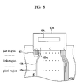
- FIG. 6 illustrates an enlarged view of wiring of the first data drive-IC in FIG. 5 .
- FIG. 5 illustrates a plan view of wiring of a liquid crystal display device in accordance with an embodiment of the present invention
- FIG. 6 illustrates an enlarged view of wiring of the first data drive-IC in FIG. 5 .
- the liquid crystal display device may include a liquid crystal display panel 60 having a first substrate 51 and a second substrate 52 opposite each other, and a liquid crystal layer (not shown) between the first and second substrates 51 and 52 .
- the liquid crystal panel 60 may have a pixel region (within the dash line) defined at a central portion of the liquid crystal panel and a non-display region (outside of the dashed line) defined on an outside of the pixel region.
- the non-display portion may include a pad region gate drive-ICs 62 and data drive-ICs 64 mounted thereon and a link region between the pixel region and the pad region through which the link wiring passes.
- the gate drive-ICs 62 and the data drive-ICs 64 may be connected to the pad region through TCP films.
- the gate drive-ICs 62 may be connected to the pad region of the liquid crystal panel 60 with first to fourth gate TCPs 61 a , 61 b , 61 c , and 61 d , respectively, and the data drive-ICs 64 may be connected to the pad region of the liquid crystal panel with first to sixth data TCP 63 a , 63 b , 63 c , 73 a , 73 b , and 73 c.
- the liquid crystal display device may be driven by a two port system, and the first to third data TCPs 63 a , 63 b , and 63 c may receive data voltage signals from a port of the system different from the fourth to sixth data TCPs 73 a , 73 b , and 73 c.
- the total number of pins of the data TCPs may not be the same as the total number of data lines 65 a on the liquid crystal panel 60 .
- the total number of output pins formed on the first to sixth data TCPs 63 a ⁇ 63 c and 73 a ⁇ 73 c may be greater than the total number of data lines 65 a formed on the pixel region.
- the number of surplus output pins of the first to sixth data TCPs 63 a ⁇ 63 c and 73 a ⁇ 73 c may be equally divided and arranged on opposite outermost sides of the pad region of the first to sixth data TCPs 63 a ⁇ 63 c and 73 a ⁇ 73 c .
- the first dummy portion 80 a including a first dummy pin may be positioned at the first data TCP 63 a .
- the second dummy portion 80 b including a second dummy pin may be positioned at the sixth data TCP 73 c .
- the link pins of the first to sixth data TCPs 63 a ⁇ 73 c which may be one to one matched and connected to the data lines 65 a between the first dummy pin and the second dummy pin, may be positioned successively.
- the SXGA class liquid crystal panel 60 has a total 3840 data lines 65 a within the pixel region (inside of the dashed line), there are a total 12 dummy output pins.
- six dummy output pins are positioned at a left outer side of the first data TCP 63 a and six dummy output pins are positioned at a right outer side of the sixth data TCP 73 c .
- the dim block caused by the dummy pins can be prevented or minimized in the neighborhood of the dummy pins.
- the first data TCP 63 a having the data drive-IC formed thereon may have 6 pins arranged from a left side in succession without connection to the pixel region, and a seventh pin may be connected to a first data line of the pixel region.
- the first data TCP 63 a may have a total 636 pins starting from the seventh pin connected to the data lines on the pixel region, starting from the first data line to a 636th data line (# 1 ⁇ # 636 ) in succession
- the second data TCP 63 b may have a total 642 pins connected to the data lines, starting from a 637th data line to a 1278th data line (# 637 ⁇ # 1278 ) without surplus
- the third data TCP 63 c may also have a total 642 pins connected to the data lines without surplus, starting from a 1279th data line to a 1920th data line (# 1279 ⁇ # 1920 ).
- the fourth data TCP 73 a may have a total 642 pins connected to the data lines, starting from a 1921st data line to a 2562nd data line (# 1921 ⁇ # 2562 ), the fifth data TCP 73 b may have a total 642 pins connected to the data lines, starting from a 2563rd data line to a 3204th data line (# 2563 ⁇ # 3204 ), and the sixth data TCP 73 c may have a total 636 pins connected to the data lines, starting from a 3205th data line to a 3840th data line (# 3205 ⁇ # 3840 ). That is, starting from the first data TCP 63 a to the sixth data TCP 73 c , the data TCPs may be connected to 636, 642, 642, 642, 642, and 636 pins in succession.
- the dummy pins not connected to the gate lines on the pixel region may be arranged on opposite (outer) sides of the gate pad region.
- the liquid crystal display device of the embodiment of the present invention has the following advantages.
- the assigning of the dummy portions having dummy pins which are not connected to the line on the pixel region to the outermost portions of the pad region prevents the difference of link resistance between the dummy portion and a neighboring portion. This enables the link resistances between link wiring to be uniform or substantially uniform. Thus, the dim block caused by resistance difference between the line wiring can be prevented or minimized. Moreover, the shifting of the dummy portions to outermost sides of the pad region is favorable in design. That is, by preventing the output pins that are not connected to the wiring from being positioned between the data lines, picture quality drop can be improved.
Landscapes
- Physics & Mathematics (AREA)
- Nonlinear Science (AREA)
- Mathematical Physics (AREA)
- Chemical & Material Sciences (AREA)
- Crystallography & Structural Chemistry (AREA)
- General Physics & Mathematics (AREA)
- Optics & Photonics (AREA)
- Liquid Crystal (AREA)
- Devices For Indicating Variable Information By Combining Individual Elements (AREA)
Abstract
Description
Claims (19)
Applications Claiming Priority (2)
| Application Number | Priority Date | Filing Date | Title |
|---|---|---|---|
| KR1020040086682A KR101066488B1 (en) | 2004-10-28 | 2004-10-28 | Liquid crystal display |
| KRP2004-86682 | 2004-10-28 |
Publications (2)
| Publication Number | Publication Date |
|---|---|
| US20060092368A1 US20060092368A1 (en) | 2006-05-04 |
| US7508480B2 true US7508480B2 (en) | 2009-03-24 |
Family
ID=36261381
Family Applications (1)
| Application Number | Title | Priority Date | Filing Date |
|---|---|---|---|
| US11/168,406 Expired - Fee Related US7508480B2 (en) | 2004-10-28 | 2005-06-29 | Liquid crystal display device with dummy portions |
Country Status (2)
| Country | Link |
|---|---|
| US (1) | US7508480B2 (en) |
| KR (1) | KR101066488B1 (en) |
Families Citing this family (4)
| Publication number | Priority date | Publication date | Assignee | Title |
|---|---|---|---|---|
| KR101649902B1 (en) * | 2009-09-29 | 2016-08-30 | 엘지디스플레이 주식회사 | Liquid crystal display device |
| KR101685409B1 (en) * | 2009-10-08 | 2016-12-13 | 엘지디스플레이 주식회사 | Array Substrate And Liquid Crystal Display Device Including The Same |
| KR20160077475A (en) * | 2014-12-23 | 2016-07-04 | 삼성디스플레이 주식회사 | Display device |
| KR102810501B1 (en) * | 2019-10-31 | 2025-05-21 | 삼성디스플레이 주식회사 | Display device |
Citations (2)
| Publication number | Priority date | Publication date | Assignee | Title |
|---|---|---|---|---|
| US5945984A (en) * | 1994-11-24 | 1999-08-31 | Kabushiki Kaisha Toshiba | Display device and method of inspecting same |
| US6278509B1 (en) * | 1997-03-26 | 2001-08-21 | Sharp Kabushiki Kaisha | Display device having particular ribs between TCPs |
Family Cites Families (1)
| Publication number | Priority date | Publication date | Assignee | Title |
|---|---|---|---|---|
| KR100864922B1 (en) * | 2002-04-20 | 2008-10-22 | 엘지디스플레이 주식회사 | LCD Display |
-
2004
- 2004-10-28 KR KR1020040086682A patent/KR101066488B1/en not_active Expired - Fee Related
-
2005
- 2005-06-29 US US11/168,406 patent/US7508480B2/en not_active Expired - Fee Related
Patent Citations (2)
| Publication number | Priority date | Publication date | Assignee | Title |
|---|---|---|---|---|
| US5945984A (en) * | 1994-11-24 | 1999-08-31 | Kabushiki Kaisha Toshiba | Display device and method of inspecting same |
| US6278509B1 (en) * | 1997-03-26 | 2001-08-21 | Sharp Kabushiki Kaisha | Display device having particular ribs between TCPs |
Also Published As
| Publication number | Publication date |
|---|---|
| KR20060037660A (en) | 2006-05-03 |
| US20060092368A1 (en) | 2006-05-04 |
| KR101066488B1 (en) | 2011-09-21 |
Similar Documents
| Publication | Publication Date | Title |
|---|---|---|
| JP4170033B2 (en) | Liquid crystal display | |
| US7113243B2 (en) | In-plane switching mode liquid crystal display device comprising common electrodes and pixel electrodes on both substrates and method of manufacturing the same | |
| US6833888B2 (en) | Liquid crystal display device including sub-pixels corresponding to red, green, blue and white color filters | |
| US10705398B2 (en) | Active matrix substrate and display panel | |
| JP3617458B2 (en) | Substrate for display device, liquid crystal device and electronic device | |
| US8068077B2 (en) | Contact structure of conductive films and thin film transistor array panel including the same | |
| US9875699B2 (en) | Display device | |
| CN102012586B (en) | Liquid crystal device and electronic apparatus | |
| US7477347B2 (en) | Liquid crystal device and electronic apparatus | |
| US8441604B2 (en) | Liquid crystal display having circular shaped protrusions on the common electrode | |
| JPH11109385A (en) | Liquid crystal display device | |
| US11106072B2 (en) | Display device | |
| US20060007086A1 (en) | Liquid crystal display device, signal transmission film, and display apparatus having the signal transmission film | |
| US10847109B2 (en) | Active matrix substrate and display panel | |
| US20050062687A1 (en) | Display device | |
| US7535519B2 (en) | Liquid crystal display and thin film transistor substrate therefor | |
| US9217888B2 (en) | Display device | |
| US7508480B2 (en) | Liquid crystal display device with dummy portions | |
| CN112764282B (en) | Array substrate, liquid crystal display panel and liquid crystal display device | |
| CN119395915B (en) | Display panel and display device | |
| KR20040103275A (en) | In-Plane Switching Mode Liquid Crystal Display device and method for fabricating the same | |
| KR20070071753A (en) | LCD Display Module | |
| CN120690111A (en) | Display panel, spliced display device and automotive display equipment | |
| JP2001051621A (en) | Electro-optical device | |
| KR20060058422A (en) | LCD Display |
Legal Events
| Date | Code | Title | Description |
|---|---|---|---|
| AS | Assignment |
Owner name: LG.PHILIPS LCD CO., LTD., KOREA, REPUBLIC OF Free format text: ASSIGNMENT OF ASSIGNORS INTEREST;ASSIGNOR:CHO, SOON DONG;REEL/FRAME:016743/0616 Effective date: 20050621 |
|
| AS | Assignment |
Owner name: LG DISPLAY CO., LTD., KOREA, REPUBLIC OF Free format text: CHANGE OF NAME;ASSIGNOR:LG.PHILIPS LCD CO., LTD.;REEL/FRAME:020985/0675 Effective date: 20080304 Owner name: LG DISPLAY CO., LTD.,KOREA, REPUBLIC OF Free format text: CHANGE OF NAME;ASSIGNOR:LG.PHILIPS LCD CO., LTD.;REEL/FRAME:020985/0675 Effective date: 20080304 |
|
| FEPP | Fee payment procedure |
Free format text: PAYOR NUMBER ASSIGNED (ORIGINAL EVENT CODE: ASPN); ENTITY STATUS OF PATENT OWNER: LARGE ENTITY |
|
| STCF | Information on status: patent grant |
Free format text: PATENTED CASE |
|
| FEPP | Fee payment procedure |
Free format text: PAYOR NUMBER ASSIGNED (ORIGINAL EVENT CODE: ASPN); ENTITY STATUS OF PATENT OWNER: LARGE ENTITY |
|
| FPAY | Fee payment |
Year of fee payment: 4 |
|
| FPAY | Fee payment |
Year of fee payment: 8 |
|
| FEPP | Fee payment procedure |
Free format text: MAINTENANCE FEE REMINDER MAILED (ORIGINAL EVENT CODE: REM.); ENTITY STATUS OF PATENT OWNER: LARGE ENTITY |
|
| LAPS | Lapse for failure to pay maintenance fees |
Free format text: PATENT EXPIRED FOR FAILURE TO PAY MAINTENANCE FEES (ORIGINAL EVENT CODE: EXP.); ENTITY STATUS OF PATENT OWNER: LARGE ENTITY |
|
| STCH | Information on status: patent discontinuation |
Free format text: PATENT EXPIRED DUE TO NONPAYMENT OF MAINTENANCE FEES UNDER 37 CFR 1.362 |
|
| FP | Lapsed due to failure to pay maintenance fee |
Effective date: 20210324 |