US7508258B2 - Amplifier circuit - Google Patents
Amplifier circuit Download PDFInfo
- Publication number
- US7508258B2 US7508258B2 US11/703,026 US70302607A US7508258B2 US 7508258 B2 US7508258 B2 US 7508258B2 US 70302607 A US70302607 A US 70302607A US 7508258 B2 US7508258 B2 US 7508258B2
- Authority
- US
- United States
- Prior art keywords
- signal
- pulse
- hold circuit
- output terminal
- amplifier
- Prior art date
- Legal status (The legal status is an assumption and is not a legal conclusion. Google has not performed a legal analysis and makes no representation as to the accuracy of the status listed.)
- Expired - Fee Related, expires
Links
Images


Classifications
-
- H—ELECTRICITY
- H03—ELECTRONIC CIRCUITRY
- H03F—AMPLIFIERS
- H03F1/00—Details of amplifiers with only discharge tubes, only semiconductor devices or only unspecified devices as amplifying elements
- H03F1/32—Modifications of amplifiers to reduce non-linear distortion
- H03F1/3211—Modifications of amplifiers to reduce non-linear distortion in differential amplifiers
-
- H—ELECTRICITY
- H03—ELECTRONIC CIRCUITRY
- H03F—AMPLIFIERS
- H03F1/00—Details of amplifiers with only discharge tubes, only semiconductor devices or only unspecified devices as amplifying elements
- H03F1/26—Modifications of amplifiers to reduce influence of noise generated by amplifying elements
-
- H—ELECTRICITY
- H03—ELECTRONIC CIRCUITRY
- H03F—AMPLIFIERS
- H03F3/00—Amplifiers with only discharge tubes or only semiconductor devices as amplifying elements
- H03F3/38—DC amplifiers with modulator at input and demodulator at output; Modulators or demodulators specially adapted for use in such amplifiers
- H03F3/387—DC amplifiers with modulator at input and demodulator at output; Modulators or demodulators specially adapted for use in such amplifiers with semiconductor devices only
-
- H—ELECTRICITY
- H03—ELECTRONIC CIRCUITRY
- H03F—AMPLIFIERS
- H03F3/00—Amplifiers with only discharge tubes or only semiconductor devices as amplifying elements
- H03F3/45—Differential amplifiers
- H03F3/45071—Differential amplifiers with semiconductor devices only
- H03F3/45076—Differential amplifiers with semiconductor devices only characterised by the way of implementation of the active amplifying circuit in the differential amplifier
- H03F3/45475—Differential amplifiers with semiconductor devices only characterised by the way of implementation of the active amplifying circuit in the differential amplifier using IC blocks as the active amplifying circuit
-
- H—ELECTRICITY
- H03—ELECTRONIC CIRCUITRY
- H03F—AMPLIFIERS
- H03F3/00—Amplifiers with only discharge tubes or only semiconductor devices as amplifying elements
- H03F3/45—Differential amplifiers
- H03F3/45071—Differential amplifiers with semiconductor devices only
- H03F3/45479—Differential amplifiers with semiconductor devices only characterised by the way of common mode signal rejection
- H03F3/45928—Differential amplifiers with semiconductor devices only characterised by the way of common mode signal rejection using IC blocks as the active amplifying circuit
- H03F3/45968—Differential amplifiers with semiconductor devices only characterised by the way of common mode signal rejection using IC blocks as the active amplifying circuit by offset reduction
- H03F3/45982—Differential amplifiers with semiconductor devices only characterised by the way of common mode signal rejection using IC blocks as the active amplifying circuit by offset reduction by using a feedforward circuit
- H03F3/45986—Differential amplifiers with semiconductor devices only characterised by the way of common mode signal rejection using IC blocks as the active amplifying circuit by offset reduction by using a feedforward circuit using switching means, e.g. sample and hold
-
- H—ELECTRICITY
- H03—ELECTRONIC CIRCUITRY
- H03F—AMPLIFIERS
- H03F3/00—Amplifiers with only discharge tubes or only semiconductor devices as amplifying elements
- H03F3/45—Differential amplifiers
- H03F3/45071—Differential amplifiers with semiconductor devices only
- H03F3/45479—Differential amplifiers with semiconductor devices only characterised by the way of common mode signal rejection
- H03F3/45928—Differential amplifiers with semiconductor devices only characterised by the way of common mode signal rejection using IC blocks as the active amplifying circuit
- H03F3/45968—Differential amplifiers with semiconductor devices only characterised by the way of common mode signal rejection using IC blocks as the active amplifying circuit by offset reduction
- H03F3/45991—Differential amplifiers with semiconductor devices only characterised by the way of common mode signal rejection using IC blocks as the active amplifying circuit by offset reduction by using balancing means
- H03F3/45995—Differential amplifiers with semiconductor devices only characterised by the way of common mode signal rejection using IC blocks as the active amplifying circuit by offset reduction by using balancing means using switching means
-
- H—ELECTRICITY
- H03—ELECTRONIC CIRCUITRY
- H03F—AMPLIFIERS
- H03F2203/00—Indexing scheme relating to amplifiers with only discharge tubes or only semiconductor devices as amplifying elements covered by H03F3/00
- H03F2203/45—Indexing scheme relating to differential amplifiers
- H03F2203/45138—Two or more differential amplifiers in IC-block form are combined, e.g. measuring amplifiers
-
- H—ELECTRICITY
- H03—ELECTRONIC CIRCUITRY
- H03F—AMPLIFIERS
- H03F2203/00—Indexing scheme relating to amplifiers with only discharge tubes or only semiconductor devices as amplifying elements covered by H03F3/00
- H03F2203/45—Indexing scheme relating to differential amplifiers
- H03F2203/45212—Indexing scheme relating to differential amplifiers the differential amplifier being designed to have a reduced offset
-
- H—ELECTRICITY
- H03—ELECTRONIC CIRCUITRY
- H03F—AMPLIFIERS
- H03F2203/00—Indexing scheme relating to amplifiers with only discharge tubes or only semiconductor devices as amplifying elements covered by H03F3/00
- H03F2203/45—Indexing scheme relating to differential amplifiers
- H03F2203/45614—Indexing scheme relating to differential amplifiers the IC comprising two cross coupled switches
-
- H—ELECTRICITY
- H03—ELECTRONIC CIRCUITRY
- H03F—AMPLIFIERS
- H03F2203/00—Indexing scheme relating to amplifiers with only discharge tubes or only semiconductor devices as amplifying elements covered by H03F3/00
- H03F2203/45—Indexing scheme relating to differential amplifiers
- H03F2203/45616—Indexing scheme relating to differential amplifiers the IC comprising more than one switch, which are not cross coupled
-
- H—ELECTRICITY
- H03—ELECTRONIC CIRCUITRY
- H03F—AMPLIFIERS
- H03F2203/00—Indexing scheme relating to amplifiers with only discharge tubes or only semiconductor devices as amplifying elements covered by H03F3/00
- H03F2203/45—Indexing scheme relating to differential amplifiers
- H03F2203/45681—Indexing scheme relating to differential amplifiers the LC comprising offset compensating means
-
- H—ELECTRICITY
- H03—ELECTRONIC CIRCUITRY
- H03F—AMPLIFIERS
- H03F2203/00—Indexing scheme relating to amplifiers with only discharge tubes or only semiconductor devices as amplifying elements covered by H03F3/00
- H03F2203/45—Indexing scheme relating to differential amplifiers
- H03F2203/45726—Indexing scheme relating to differential amplifiers the LC comprising more than one switch, which are not cross coupled
Definitions
- the present invention relates to a chopper amplifier circuit capable of reducing a DC offset and noise in an amplifier, and more particularly, to a chopper amplifier circuit capable of reducing an influence of spike noise.
- a chopper amplifier circuit has widely been used as a low-noise low-drift DC amplifier.
- a conventional chopper amplifier includes, as shown in FIG. 9A , an amplifier 1 and chopper circuits 11 and 12 provided at a preceding stage and a subsequent stage of the amplifier 1 , respectively, so as to attain low-noise amplification.
- the chopper circuit 11 employs four switching means, which are turned on and off in accordance with pulses ⁇ 1 and ⁇ 2 shown in FIG. 9B .
- the pulses ⁇ 1 and ⁇ 2 are rectangular pulses shifted in phase.
- the switching means are controlled in a cycle based on the pulses ⁇ 1 and ⁇ 2 so as to determine which of input signals inputted to input terminals 15 and 16 is inputted to which of a plus (+) input terminal and a minus ( ⁇ ) input terminal of the amplifier 1 .
- a line connection status of the circuit changes as follows.
- the chopper circuit 11 includes switches 11 a and 11 b which are controlled by the pulse ⁇ 1 and switches 11 c and 11 d which are controlled by the pulse ⁇ 2 .
- the pulse ⁇ 1 is at the level “H” while the pulse ⁇ 2 is at the level “L”. Accordingly, the switches 11 a and 11 b are turned on and the switches 11 c and 11 d are turned off. In this state, the input terminal 15 is connected to the plus (+) input terminal of the amplifier 1 , and the input terminal 16 is connected to the minus ( ⁇ ) input terminal of the amplifier 1 .
- the pulse ⁇ 1 is at the level “L” while the pulse ⁇ 2 is at the level “H”. Accordingly, the switches 11 a and 11 b are turned off and the switches 11 c and 11 d are turned on. In this state, the input terminal 15 is connected to the minus ( ⁇ ) input terminal of the amplifier 1 , and the input terminal 16 is connected to the plus (+) input terminal of the amplifier 1 .
- the chopper circuit 12 also employs four switching means, which are turned on and off in accordance with the rectangular pulses ⁇ 1 and ⁇ 2 shifted in phase.
- the switching means are controlled in a cycle based on the pulses ⁇ 1 and ⁇ 2 so as to determine which of output signals outputted from a plus (+) output terminal 30 and a minus ( ⁇ ) output terminal 31 of the amplifier 1 is inputted to which of output terminals 17 and 18 .
- a line connection status of the circuit changes as follows.
- the chopper circuit 12 includes switches 12 a and 12 b which are controlled by the pulse ⁇ 1 and switches 12 c and 12 d which are controlled by the pulse ⁇ 2 .
- the pulse ⁇ 1 is at the level “H” while the pulse ⁇ 2 is at the level “L”. Accordingly, the switches 12 a and 12 b are turned on and the switches 12 c and 12 d are turned off. In this state, the plus (+) output terminal 30 of the amplifier 1 is connected to the output terminal 17 , and the minus ( ⁇ ) output terminal 31 of the amplifier 1 is connected to the output terminal 18 .
- the pulse ⁇ 1 is at the level “L” while the pulse ⁇ 2 is at the level “H”. Accordingly, the switches 12 a and 12 b are turned off and the switches 12 c and 12 d are turned on. In this state, the minus ( ⁇ ) output terminal 31 of the amplifier 1 is connected to the output terminal 17 , and the plus (+) output terminal 30 of the amplifier 1 is connected to the output terminal 18 .
- FIGS. 10A to 10F are graphs each showing frequency characteristics at each portion (vertical axis: amplitude, horizontal axis: frequency).
- FIG. 10G shows the pulses ( ⁇ 1 and ⁇ 2 of FIG. 9B which are inputted to the chopper circuits 11 and 12 .
- the amplifier 1 has input conversion noise and an offset voltage Vn shown in FIG. 10C .
- the chopper circuits 11 and 12 each modulate a signal through chopper processing based on the frequency of the pulses ⁇ 1 and ⁇ 2 (a rectangular wave of frequency fc).
- an input signal vin inputted with frequency characteristics of FIG. 10A is subjected to modulation at the chopper circuit 11 based on the pulses ⁇ 1 and ⁇ 2 , so as to be converted into a modulated signal of frequency characteristics shown in FIG. 10B .
- the input signal is modulated to have a frequency of an odd-multiple of the frequency of the pulses ⁇ 1 and ⁇ 2 which control the chopper processing performed in the chopper circuit 11 .
- the input conversion noise and the offset voltage Vn of FIG. 10C are superimposed on (added to) the modulated signal to be outputted from the amplifier 1 as an amplified signal shown in FIG. 10D .
- the chopper circuit 12 demodulates the amplified signal into the frequency band of the input signal (low-frequency range including direct current) based on the pulses ⁇ 1 and ⁇ 2 , and outputs the signal as an output signal of frequency characteristics shown in FIG. 1E .
- the chopper circuit 12 modulates the input conversion noise and the offset voltage Vn of the amplifier 1 to have a frequency of an odd-multiple of the frequency of the pulses ⁇ 1 and ⁇ 2 used for the demodulation.
- the output signal outputted from the chopper circuit 12 eventually includes a frequency component of an odd-multiple of the frequency of the pulses ⁇ 1 and ⁇ 2 .
- a low-pass filter 13 is provided at an output stage, to thereby obtain an output signal having frequency characteristics shown in FIG. 10F (see, for example, P. Allen and D. R. Holberg, CMOS Analog Circuit Design, pp. 490-494, Saunders College Publishing, 1987, hereinafter referred to as Non-Patent Document 1).
- the chopper amplifier circuit described above suppresses an influence of the input conversion noise and the offset voltage Vn of the amplifier 1 to thereby amplify only the frequency component of an input signal.
- Non-Patent Document 1 has a drawback in that it is impossible to completely remove spike components included in the output signal through the low-pass filter 13 , leading to a harmonic distortion.
- the spike components are generated in the output signal due to the following mechanism.
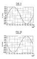
- the input terminal 15 is supplied with an input signal having a sinusoidal wave shown in FIG. 11
- the input terminal 16 is supplied with an input signal having a sinusoidal wave shown in FIG. 12 .
- the vertical axis is a voltage scale and the horizontal axis is a time scale.
- the input signal is modulated at the chopper circuit 11 , amplified by the amplifier 1 , and demodulated at the chopper circuit 12 , before being outputted from the output terminal 17 as an output signal.
- FIG. 13 shows the output signal thus outputted.
- the vertical axis is a voltage scale and the horizontal axis is a time scale.
- FIG. 14 shows an amplified signal outputted from the plus (+) output terminal 30 of the amplifier 1
- FIG. 15 shows an amplified signal outputted from the minus ( ⁇ ) output terminal 31 .
- the vertical axis is a voltage scale and the horizontal axis is a time scale.
- the chopper circuit 12 samples the amplified signal of FIG. 14 which has been outputted from the plus (+) output terminal 30 , and outputs the signal.
- the chopper circuit 12 samples the amplified signal of FIG. 15 which has been outputted from the minus ( ⁇ ) output terminal 31 , and outputs the signal.
- the present invention has been made in view of the above-mentioned circumstances, and therefore, it is an object of the present invention to provide a chopper amplifier circuit capable of obtaining an output signal obtained from an input signal alone, the output signal having no harmonic distortion as compared with a conventional example, by eliminating an influence of a slew rate of an amplifier and suppressing spike generation.
- a chopper amplifier circuit including: a chopper circuit for chopping an input signal based on a pulse having a predetermined frequency so as to modulate the input signal; an amplifier for amplifying the input signal thus modulated; a first sample hold circuit; and a second sample hold circuit, in which: the chopper amplifier circuit demodulates the modulated signal thus amplified, and outputs the signal thus amplified as an output signal; the chopper circuit chops the input signal by a first pulse and a second pulse shifted from each other in phase by a half cycle, switches a relation of connection between an input terminal pair and an output terminal pair at a timing of the chopping (for example, according to an embodiment of the present invention, the timing at which a pulse ⁇ 1 shifts from a level “H” to a level “L” and a pulse ⁇ 2 shifts from the level “L” to the level “H”, or the pulse ⁇
- the first sample hold circuit and the second sample hold circuit each include: a first switch pair into which the amplified signal is inputted; a hold circuit for holding a voltage level of the amplified signal inputted from the first switch pair; and a second switch pair for controlling an output of the amplified signal held by the hold circuit, one of the first switch pair and the second switch pair being turned off while the other one of the first switch pair and the second switch pair is turned on.
- the input terminal pair is composed of a first input terminal and a second input terminal
- the output terminal pair is composed of a first output terminal and a second output terminal.
- the first input terminal and the first output terminal are connected to each other and the second input terminal and the second output terminal are connected to each other, when the first pulse is inputted
- the first input terminal and the second output terminal are connected to each other and the second input terminal and the first output terminal are connected to each other, when the second pulse is inputted.
- the first sample hold circuit and the second sample hold circuit each hold a voltage level of the amplified signal due to a configuration of a switched capacitor.
- the first switch pair and the second switch pair which have output terminals connected to each other, each synthesize the amplified signals outputted from each hold circuit in each of the first sample hold circuit and the second sample hold circuit based on the first pulse and the second pulse, and output the synthesized signal as an output signal.
- a switch matrix of the chopper circuit is changed based on the first and second pulses shifted in phase by a half cycle, the relation of connection between the input terminal and the output terminal is switched, and a modulated signal obtained by chopping an input signal is amplified, before the amplified signal is alternately sampled and held at two sample hold circuits, i.e., the first and second sample hold circuits based on the first and second pulses.
- the other sample hold circuit samples the output signal from the amplifier, to thereby output an output signal obtained by synthesizing (demodulating) amplified signals outputted from the amplifier for every half cycle, the amplified signals being shifted from one another by a half cycle.
- the amplified signal is read out from the hold circuit at a timing shifted by a half cycle from a timing at which the amplified signal from the amplifier is sampled, to thereby output the amplified signal in a state where the output is completely stable. Accordingly, it is possible to suppress spike generation by eliminating the influence of the slew rate of the amplifier when synthesizing the amplified signal.
- the chopper amplifier circuit of the present invention is provided with the sample hold circuit connected in tandem at a subsequent stage of the amplifier, so the amplified signal outputted from the amplifier is temporarily held to eliminate the influence of the slew rate of the amplifier so as to prevent spike component generation, thereby producing an effect of reducing a harmonic distortion included in the output signal which has been outputted through the low-pass filter, as compared with the conventional example.
- FIG. 2 is a waveform chart of an amplified signal outputted from a plus (+) output terminal ( 20 ) of an amplifier ( 1 ) shown in FIG. 1 ;
- FIG. 3 is a waveform chart of an amplified signal outputted from a minus ( ⁇ ) output terminal ( 21 ) of the amplifier ( 1 ) shown in FIG. 1 ;
- FIG. 4 is a waveform chart of a signal outputted from an output terminal ( 22 ) of a hold circuit ( 26 ) shown in FIG. 1 ;
- FIG. 6 is a waveform chart of an output signal outputted from an output terminal ( 17 ) shown in FIG. 1 ;
- FIG. 7 is a waveform chart of an output signal outputted from an output terminal ( 18 ) shown in FIG. 1 ;
- FIG. 8 is a block diagram showing in detail the configuration example of the chopper amplifier circuit according to the embodiment of the present invention.
- FIG. 9A is a block diagram showing a configuration of a conventional chopper amplifier circuit
- FIG. 9B is a diagram for explaining pulses ( ⁇ 1 and ⁇ 2 );
- FIG. 11 is a waveform chart showing a waveform of an input signal to be inputted to an input terminal ( 15 );
- FIG. 12 is a waveform chart showing a waveform of an input signal to be inputted to an input terminal ( 16 );
- FIG. 13 is a waveform chart showing a waveform of an output signal to be outputted from the output terminal ( 17 ) of FIG. 9A ;
- FIG. 14 is a waveform chart showing a waveform of an amplified signal outputted from a plus (+) output terminal ( 30 ) of the amplifier ( 1 ) of FIG. 9A ;
- FIG. 15 is a waveform chart showing a waveform of an amplified signal outputted from a minus ( ⁇ ) output terminal ( 31 ) of the amplifier ( 1 ) of FIG. 9A .
- FIG. 1 is a block diagram showing a configuration example of the chopper amplifier circuit according to this embodiment.
- a chopper circuit 11 and an amplifier 1 are similar to those in the conventional example of FIG. 9A .
- the circuit of FIG. 1 is different from the conventional example in that the circuit includes sample hold circuits 2 and 3 connected in parallel, in place of the chopper circuit 12 in the conventional example, at the subsequent stage of the amplifier 1 .
- the circuit of this embodiment operates similarly to the conventional example, so a brief explanation is given on a configuration of the chopper circuit 11 .
- the chopper circuit 11 includes a switch matrix formed of switches 11 a , 11 b , 11 c , and 11 d .
- the switches 11 a and 11 b are turned on when a pulse ⁇ 1 is at the level “H” while the switches 11 c and 11 d are turned on when a pulse ⁇ 2 is at the level “H”.
- the switch 11 a is provided between an input terminal 15 and a plus (+) input terminal of the amplifier 1
- the switch 11 b is provided between an input terminal 16 and a minus ( ⁇ ) input terminal of the amplifier 1
- the switch 11 c is provided between the input terminal 15 and the minus ( ⁇ ) input terminal of the amplifier 1
- the switch 11 d is provided between the input terminal 16 and the plus (+) input terminal of the amplifier 1 .
- the sample hold circuit 2 holds voltage levels of a plus (+) output terminal 20 and a minus ( ⁇ ) output terminal 21 of the amplifier 1 when the pulse ⁇ 1 is at the level “H” and the pulse ⁇ 2 is at the level “L”, and outputs the voltage levels thus held when the pulse ⁇ 1 is at the level “L” and the pulse ⁇ 2 is at the level “H”.
- the sample hold circuit 2 holds voltage levels of the plus (+) output terminal (positive side output terminal) 20 and the minus ( ⁇ ) output terminal (negative side output terminal) 21 of the amplifier 1 when the pulse ⁇ 1 is at the level “L” and the pulse ⁇ 2 is at the level “H”, and outputs the voltage levels thus held when the pulse ⁇ 11 is at the level “H” and the pulse ⁇ 2 is at the level “L”.
- the sample hold circuit 2 includes switches 28 a and 28 b which constitute an input switch pair on the input side, a hold circuit 26 , and switches 28 c and 28 d which constitute an output switch pair on the output side.
- the switch 28 a which is provided in series between the amplifier 1 and the hold circuit 26 , connects to the plus (+) output terminal 20 of the amplifier 1 at the input side terminal thereof and to an input terminal 26 a of the hold circuit 26 at the output side terminal thereof.
- the switch 28 b which is provided in series between the amplifier 1 and the hold circuit 26 , connects to the minus ( ⁇ ) output terminal 21 of the amplifier 1 at the input side terminal thereof and to an input terminal 26 b of the hold circuit 26 at the output side terminal thereof.
- the switch 28 c which is provided in series between the hold circuit 26 and an output terminal 17 , connects to the output terminal 22 (positive side output terminal) of the hold circuit 26 at the input side terminal thereof and to the output terminal 17 at the output side terminal thereof.
- the switch 28 d which is provided in series between the hold circuit 26 and an output terminal 18 , connects to the output terminal 23 (negative side output terminal) of the hold circuit 26 at the input side terminal thereof and to the output terminal 18 at the output side terminal thereof.
- the switches 28 a and 28 b are turned on when the pulse ⁇ 1 is at the level “H” and turned off when the pulse ⁇ 2 is at the level “H”.
- the switches 28 c and 28 d are turned off when the pulse ⁇ 1 is at the level “H” and turned on when the pulse ⁇ 2 is at the level “H”.
- the sample hold circuit 3 includes switches 29 a and 29 b which constitute an input switch pair on the input side, a hold circuit 27 , and switches 29 c and 29 d which constitute an output switch pair on the output side.
- the switch 29 a which is provided in series between the amplifier 1 and the hold circuit 27 , connects to the minus ( ⁇ ) output terminal 21 of the amplifier 1 at the input side terminal thereof and to an input terminal 27 a of the hold circuit 27 at the output side terminal thereof.
- the switch 29 b which is provided in series between the amplifier 1 and the hold circuit 27 , connects to the plus (+) output terminal 20 of the amplifier 1 at the input side terminal thereof and to an input terminal 27 b of the hold circuit 27 at the output side terminal thereof.
- the switch 29 c which is provided in series between the hold circuit 27 and an output terminal 17 , connects to the output terminal 24 (negative side output terminal) of the hold circuit 27 at the input side terminal thereof and to the output terminal 17 at the output side terminal thereof.
- the switch 29 d which is provided in series between the hold circuit 27 and the output terminal 18 , connects to the output terminal 25 (positive side output terminal) of the hold circuit 27 at the input side terminal thereof and to the output terminal 18 at the output side terminal thereof.
- the switches 29 a and 29 b are turned off when the pulse ⁇ 1 is at the level “H” and turned on when the pulse ⁇ 2 is at the level “H”.
- the switches 29 c and 29 d are turned on when the pulse ⁇ 1 is at the level “H” and turned off when the pulse ⁇ 2 is at the level “H”.
- the input terminal 15 is supplied with an input signal having a sinusoidal wave shown in FIG. 11
- the input terminal 16 is supplied with an input signal having a sinusoidal wave shown in FIG. 12 .
- Operations of the chopper circuit 11 and the amplifier 1 are similar to those of the conventional example, and therefore explanations thereof are omitted.
- the pulses ⁇ 1 and ⁇ 2 are shifted (different) from each other in phase by a half cycle, that is, “ ⁇ (180 degrees)”.
- Each of the input signals is modulated at the chopper circuit 11 , amplified by the amplifier 1 up to a predetermined magnification of, for example, 10 times, and outputted to the plus (+) output terminal 20 and the minus ( ⁇ ) output terminal 21 .
- the voltage difference Voutp having a signal waveform of FIG. 2 is outputted from the plus (+) terminal 20 of the amplifier 1
- the voltage difference Voutn having a signal waveform of FIG. 3 is outputted from the minus ( ⁇ ) terminal 21 of the amplifier 1 .
- the vertical axis is a voltage scale and the horizontal axis is a time scale.
- the hold circuit 26 has the input terminal 26 a connected to the plus (+) side output terminal 20 of the amplifier 1 and the input terminal 26 b connected to the minus ( ⁇ ) side output terminal 21 of the amplifier 1 .
- the hold circuit 26 holds the voltage difference Voutp inputted from the input terminal 26 a and outputs the voltage difference Voutp from the output terminal 22 .
- the hold circuit 26 also holds the voltage difference Voutn inputted from the input terminal 26 b and outputs the voltage difference Voutn from the output terminal 23 .
- the switches 28 c and 28 d constituting the output switch pair of the sample hold circuit 2 are turned off, and accordingly, the sample hold circuit 2 does not output the voltage levels outputted from the hold circuit 26 to the output terminals 17 and 18 as output signals.
- the sample hold circuit 2 is sampling the voltage levels of the amplified signals from the amplifier 1 .
- the hold circuit 27 has the output terminal 24 connected to the output terminal 17 and the output terminal 25 connected to the output terminal 18 .
- the hold circuit 27 outputs the voltage difference Voutn thus held to the output terminal 17 through the output terminal 24 .
- the hold circuit 27 outputs the voltage difference Voutp thus held to the output terminal 18 through the output terminal 25 .
- the switches 29 a and 29 b constituting the input switch pair of the sample hold circuit 3 are turned off, and accordingly, the voltage levels of the amplified signals outputted by the amplifier 1 are not inputted to the input terminals 27 a and 27 b of the hold circuit 27 , which means that the hold circuit 27 is in a holding state.
- the sample hold circuit 3 is outputting the voltage levels of the amplified signals held in the hold circuit 27 .
- the hold circuit 26 has the output terminal 22 connected to the output terminal 17 and the output terminal 23 connected to the output terminal 18 .
- the hold circuit 26 outputs the voltage difference Voutp thus held to the output terminal 17 through the output terminal 22 .
- the hold circuit 26 outputs the voltage difference Voutn thus held to the output terminal 18 through the output terminal 23 .
- the switches 28 a and 28 b constituting the input switch pair of the sample hold circuit 2 are turned off, and accordingly, the voltage levels of the amplified signals outputted by the amplifier 1 are not inputted to the input terminals 26 a and 26 b of the hold circuit 26 , which means that the hold circuit 26 is in a holding state.
- the sample hold circuit 2 is outputting the voltage levels of the amplified signals held in the hold circuit 26 .
- the hold circuit 27 has the input terminal 27 a connected to the minus ( ⁇ ) side output terminal 21 of the amplifier 1 and the input terminal 27 b connected to the plus (+) side output terminal 20 of the amplifier 1 .
- the hold circuit 27 holds the voltage difference Voutn inputted from the input terminal 27 a and outputs the voltage difference Voutn from the output terminal 24 .
- the hold circuit 27 also holds the voltage difference Voutp inputted from the input terminal 27 b and outputs the voltage difference Voutp from the output terminal 25 .
- the switches 29 c and 29 d constituting the output switch pair of the sample hold circuit 3 are turned off, and accordingly, the sample hold circuit 3 does not output the voltage levels outputted from the hold circuit 27 to the output terminals 17 and 18 as output signals.
- the sample hold circuit 3 is sampling the voltage levels of the amplified signals from the amplifier 1 .
- one of the sample hold circuit 2 and the sample hold circuit 3 outputs the voltage levels held in the other one of the circuits while the other one of the sample hold circuit 2 and the sample hold circuit 3 is sampling the voltage levels, depending on which one of the pulses ⁇ 1 and 2 ⁇ is inputted at the level “H”.
- the sample hold circuits 2 and 3 take turns sampling and outputting for every half cycle.
- FIG. 4 shows a signal waveform of a signal outputted from the output terminal 22 in the manner as described above, which is a positive side output terminal of the hold circuit 26 .
- the vertical axis is a voltage scale and the horizontal axis is a time scale.
- the output signal outputted from the output terminal 22 bears a large spike component when the pulse ⁇ 2 changes from the level “H” to the level “L” and the pulse ⁇ 1 changes from the level “L” to the level “H”.
- the output signal outputted from the output terminal 22 hardly bears a spike component when the pulse ⁇ 2 changes from the level “L” to the level “H” and the pulse ⁇ 1 changes from the level “H” to the level “L”.
- the voltage held in the hold circuit 26 greatly fluctuates when the hold circuit 26 samples the amplified signals at the pulse ⁇ 1 because of a spike component generated due to the slew rate of the amplifier 1 .
- the hold circuit 26 outputs the amplified signal held in the circuit to the output terminal 17 at the pulse ⁇ 2 through the switch 28 c , the output signal is only affected by the voltage fluctuation due to switching noise or the like at the switch 28 c without being affected at all by the slew rate of the amplifier 1 . Therefore, the output signal outputted from the sample hold circuit 2 bears no spike component.
- FIG. 5 shows a signal waveform of a signal outputted from the output terminal 24 , which is a negative side output terminal of the hold circuit 27 .
- the vertical axis is a voltage scale and the horizontal axis is a time scale.
- the output signal outputted from the output terminal 24 bears a large spike component when the pulse ⁇ 1 changes from the level “H” to the level “L” and the pulse ⁇ 2 changes from the level “L” to the level “H”.
- the output signal outputted from the output terminal 24 hardly bears a spike component when the pulse ⁇ 1 changes from the level “L” to the level “H” and the pulse ⁇ 2 changes from the level “H” to the level “L”.
- the voltage held in the hold circuit 27 greatly fluctuates when the hold circuit 27 samples the amplified signals at the pulse ⁇ 2 because of a spike component generated due to the slew rate of the amplifier 1 .
- the hold circuit 27 outputs the amplified signal held in the circuit to the output terminal 18 at the pulse ⁇ 1 through the switch 29 d , the output signal is only affected by the voltage fluctuation due to switching noise or the like at the switch 29 d without being affected at all by the slew rate of the amplifier 1 . Therefore, the output signal outputted from the sample hold circuit 3 bears no spike component.
- the pulse ⁇ 2 is at the level “H” and the pulse ⁇ 1 is at the level “L”
- the output signal from the output terminal 22 of the hold circuit 26 is outputted to the output terminal 17 while the output signal from the output terminal 23 of the hold circuit 26 is outputted to the output terminal 18 , due to the control performed over the switches in the sample hold circuits 2 and 3 based on the pulses ⁇ 1 and ⁇ 2 .
- the sample hold circuits 2 and 3 alternately output signals in accordance with the timings of the pulses ⁇ 1 and ⁇ 2 and synthesize the signals to produce an output signal to be outputted.
- the output signal thus obtained is outputted from the output terminal 17 .
- the output signal exhibits a sinusoidal waveform as shown in FIG. 6 without bearing large spike components shown in FIGS. 4 and 5 .
- the sample hold circuits 2 and 3 alternately output signals in accordance with the timings of the pulses ⁇ 1 and ⁇ 2 and synthesize the signal to produce an output signal be outputted.
- the output signal thus obtained is outputted from the output terminal 18 .
- the output signal exhibits a sinusoidal waveform as shown in FIG. 7 without bearing large spike components shown in FIGS. 4 and 5 .
- the vertical axis is a voltage scale and the horizontal axis is a time scale.
- the chopper amplifier circuit which includes the sample hold circuits 2 and 3 , it is possible to significantly reduce the harmonic distortion in the output signal which has been obtained by chopping an input signal and synthesizing the signal after amplification, as compared with the conventional example.
- the above-mentioned hold circuit 26 may be composed of two hold portions as shown in FIG. 8 .
- One of the hold portions holds the voltage level of the plus (+) side output terminal 20 of the amplifier 1 and is composed of a capacitor 261 and an operational amplifier 262 .
- the other one of the hold portions holds the voltage level of the minus ( ⁇ ) side output terminal 21 of the amplifier 1 and is composed of a capacitor 263 and an operational amplifier 264 .
- the above-mentioned hold circuit 27 may be composed of two hold portions as shown in FIG. 8 .
- One of the hold portions holds the voltage level of the minus ( ⁇ ) side output terminal 21 of the amplifier 1 and is composed of a capacitor 271 and an operational amplifier 272 .
- the other one of the hold portions holds the voltage level of the plus (+) side output terminal 20 of the amplifier 1 and is composed of a capacitor 273 and an operational amplifier 274 .
- the capacitor 261 is connected at one end thereof to the plus (+) input terminal of the operational amplifier 262 while connected to the ground at the other end thereof.
- the capacitor 263 is connected at one end thereof to the minus ( ⁇ ) output terminal of the operational amplifier 262 while connected to the ground at the other end thereof.
- the capacitor 261 holds the voltage level of the output terminal 20 of the amplifier 1 when the switch 28 a is turned on, and the capacitor 263 holds the voltage level of the output terminal 21 of the amplifier 1 when the switch 28 b is turned on.
- the capacitor 271 is connected at one end thereof to the plus (+) input terminal of the operational amplifier 272 while connected to the ground at the other end thereof.
- the capacitor 273 is connected at one end thereof to the plus (+) input terminal of the operational amplifier 274 while connected to the ground at the other end thereof.
- the capacitor 271 holds the voltage level of the output terminal 21 of the amplifier 1 when the switch 29 a is turned on, and the capacitor 273 holds the voltage level of the output terminal 20 of the amplifier 1 when the switch 29 b is turned on.
- the configurations of the sample hold circuits 2 and 3 are not limited to the above-mentioned configurations each using the hold circuits 26 and 27 , respectively.
- the same effect as the above-mentioned embodiment can be obtained by using another sample hold circuit as long as the sample hold circuit has a gain equal to or larger than 1.
- the amplifier 1 of FIG. 8 has an amplification factor of 10 times.
- a resistor Ic of 90 k ⁇ is provided between an output terminal (output terminal 20 ) and a minus ( ⁇ ) side input terminal of an operational amplifier 1 a .
- the operational amplifier 1 a is connected at an input terminal on the plus (+) side thereof to the output side terminal of the switch 11 a .
- a resistor 1 d of 90 k ⁇ is provided between an output terminal (output terminal 21 ) and a plus (+) side input terminal of an operational amplifier 1 b .
- the operational amplifier 1 b is connected at an input terminal on the minus ( ⁇ ) side thereof to the output side terminal of the switch 11 b .
- a resistor 1 e of 20 k ⁇ is provided between a minus ( ⁇ ) side input terminal of the operational amplifier 1 a and a plus (+) side input terminal of the operational amplifier 1 b .
- the amplification factor and the configuration of the amplifier 1 are not limited thereto.
Landscapes
- Engineering & Computer Science (AREA)
- Power Engineering (AREA)
- Physics & Mathematics (AREA)
- Nonlinear Science (AREA)
- Amplifiers (AREA)
- Manipulation Of Pulses (AREA)
Abstract
Description
Claims (4)
Applications Claiming Priority (2)
| Application Number | Priority Date | Filing Date | Title |
|---|---|---|---|
| JP2006029138A JP2007214613A (en) | 2006-02-07 | 2006-02-07 | Amplifier circuit |
| JPJP2006-029138 | 2006-02-07 |
Publications (2)
| Publication Number | Publication Date |
|---|---|
| US20070222509A1 US20070222509A1 (en) | 2007-09-27 |
| US7508258B2 true US7508258B2 (en) | 2009-03-24 |
Family
ID=38492704
Family Applications (1)
| Application Number | Title | Priority Date | Filing Date |
|---|---|---|---|
| US11/703,026 Expired - Fee Related US7508258B2 (en) | 2006-02-07 | 2007-02-06 | Amplifier circuit |
Country Status (5)
| Country | Link |
|---|---|
| US (1) | US7508258B2 (en) |
| JP (1) | JP2007214613A (en) |
| KR (1) | KR101141567B1 (en) |
| CN (1) | CN101102094B (en) |
| TW (1) | TWI392223B (en) |
Cited By (2)
| Publication number | Priority date | Publication date | Assignee | Title |
|---|---|---|---|---|
| WO2024097273A1 (en) * | 2022-11-02 | 2024-05-10 | Texas Instruments Incorporated | Auto zero techniques for high voltage analog front-end with robust ac common-mode rejection |
| US12456956B2 (en) | 2022-01-25 | 2025-10-28 | Kabushiki Kaisha Toshiba | Chopper stabilized amplifier |
Families Citing this family (19)
| Publication number | Priority date | Publication date | Assignee | Title |
|---|---|---|---|---|
| WO2009035665A1 (en) * | 2007-09-14 | 2009-03-19 | Analog Devices, Inc. | Improved low power, low noise amplifier system |
| CN101598952B (en) * | 2008-06-02 | 2011-12-07 | 联咏科技股份有限公司 | Current generator |
| JP5295941B2 (en) * | 2009-12-22 | 2013-09-18 | 株式会社豊田中央研究所 | Signal processing circuit |
| KR101154240B1 (en) * | 2010-09-15 | 2012-06-18 | 강원대학교산학협력단 | Apparatus and method for processing sensor signal for usn |
| JP5612501B2 (en) * | 2011-02-03 | 2014-10-22 | 株式会社豊田中央研究所 | Chopper type amplifier circuit |
| CN102778910A (en) * | 2011-05-08 | 2012-11-14 | 曹先国 | High voltage reference |
| JP5744658B2 (en) * | 2011-07-20 | 2015-07-08 | セイコーインスツル株式会社 | Photodetector |
| JP6158532B2 (en) * | 2013-02-26 | 2017-07-05 | エスアイアイ・セミコンダクタ株式会社 | Operational amplifier circuit |
| JP6212922B2 (en) * | 2013-04-23 | 2017-10-18 | 株式会社リコー | Chopper amplifier |
| CN103874300A (en) * | 2014-03-31 | 2014-06-18 | 太仓电威光电有限公司 | Method and system for adjusting parameters of output end of LED drive |
| CN104065266B (en) * | 2014-07-11 | 2017-12-15 | 成都芯源系统有限公司 | Control circuit for voltage converter |
| JP6796953B2 (en) * | 2016-06-02 | 2020-12-09 | エイブリック株式会社 | Amplifier circuit and multipath nested mirror amplifier circuit |
| JP6733381B2 (en) * | 2016-07-15 | 2020-07-29 | セイコーエプソン株式会社 | Physical quantity detection circuit, physical quantity detection device, electronic device and moving body |
| CN107332524B (en) * | 2017-07-12 | 2020-11-03 | 华大半导体有限公司 | Operational amplifier for suppressing low frequency noise |
| CN109450384A (en) * | 2018-09-20 | 2019-03-08 | 天津大学 | A kind of reading circuit based on chopping modulation and correlated-double-sampling |
| CN110492886B (en) * | 2019-08-20 | 2024-02-13 | 深圳市锐能微科技有限公司 | Analog-to-digital converters and analog-to-digital conversion methods |
| JP7450362B2 (en) * | 2019-10-23 | 2024-03-15 | エイブリック株式会社 | amplifier |
| JP7715499B2 (en) * | 2020-12-25 | 2025-07-30 | 日清紡マイクロデバイス株式会社 | Amplification equipment |
| CN117394809B (en) * | 2023-12-07 | 2024-03-26 | 杭州晶华微电子股份有限公司 | Fully differential instrumentation amplifier circuit, instrumentation amplifier, and integrated circuit |
Citations (1)
| Publication number | Priority date | Publication date | Assignee | Title |
|---|---|---|---|---|
| US5621319A (en) * | 1995-12-08 | 1997-04-15 | Allegro Microsystems, Inc. | Chopped hall sensor with synchronously chopped sample-and-hold circuit |
Family Cites Families (7)
| Publication number | Priority date | Publication date | Assignee | Title |
|---|---|---|---|---|
| JPS5592007A (en) | 1978-12-29 | 1980-07-12 | Chino Works Ltd | Signal processing unit |
| GB2256551B (en) * | 1991-06-06 | 1996-01-24 | Crystal Semiconductor Corp | Switched capacitor integrator with chopper stabilisation performed at the sampling rate |
| JP2605603Y2 (en) * | 1997-12-24 | 2000-07-31 | 関西日本電気株式会社 | Semiconductor integrated circuit |
| JP3105862B2 (en) * | 1998-02-27 | 2000-11-06 | 日本電気株式会社 | Voltage comparison circuit |
| DE10117384B4 (en) * | 2001-04-06 | 2004-10-07 | Infineon Technologies Ag | sensor device |
| EP1579571B1 (en) * | 2002-12-18 | 2009-04-01 | Nxp B.V. | Phase corrected miller compensation of chopper and nested chopper amplifiers |
| US7262654B2 (en) * | 2005-01-14 | 2007-08-28 | Cirrus Logic, Inc. | Circuits and methods for minimizing chopping artifacts at the output of a chopper-stabilized operational amplifier |
-
2006
- 2006-02-07 JP JP2006029138A patent/JP2007214613A/en active Pending
-
2007
- 2007-02-05 KR KR1020070011381A patent/KR101141567B1/en not_active Expired - Fee Related
- 2007-02-06 US US11/703,026 patent/US7508258B2/en not_active Expired - Fee Related
- 2007-02-06 TW TW096104297A patent/TWI392223B/en not_active IP Right Cessation
- 2007-02-07 CN CN200710005210XA patent/CN101102094B/en not_active Expired - Fee Related
Patent Citations (1)
| Publication number | Priority date | Publication date | Assignee | Title |
|---|---|---|---|---|
| US5621319A (en) * | 1995-12-08 | 1997-04-15 | Allegro Microsystems, Inc. | Chopped hall sensor with synchronously chopped sample-and-hold circuit |
Non-Patent Citations (1)
| Title |
|---|
| P. Allen and D.R. Holberg, "CMOS Analog Circuit Design," pp. 490-494, Saunders College Publishing, 1987. |
Cited By (2)
| Publication number | Priority date | Publication date | Assignee | Title |
|---|---|---|---|---|
| US12456956B2 (en) | 2022-01-25 | 2025-10-28 | Kabushiki Kaisha Toshiba | Chopper stabilized amplifier |
| WO2024097273A1 (en) * | 2022-11-02 | 2024-05-10 | Texas Instruments Incorporated | Auto zero techniques for high voltage analog front-end with robust ac common-mode rejection |
Also Published As
| Publication number | Publication date |
|---|---|
| TWI392223B (en) | 2013-04-01 |
| US20070222509A1 (en) | 2007-09-27 |
| JP2007214613A (en) | 2007-08-23 |
| CN101102094A (en) | 2008-01-09 |
| KR101141567B1 (en) | 2012-05-16 |
| KR20070080565A (en) | 2007-08-10 |
| CN101102094B (en) | 2011-08-10 |
| TW200737692A (en) | 2007-10-01 |
Similar Documents
| Publication | Publication Date | Title |
|---|---|---|
| US7508258B2 (en) | Amplifier circuit | |
| US20190158034A1 (en) | Chopper amplifiers with high pass filter for suppressing chopping ripple | |
| EP2327153B1 (en) | Auto-correction feedback loop for offset and ripple suppression in a chopper-stabilized amplifier | |
| US20090115522A1 (en) | Low power, low noise amplifier system | |
| US9172332B2 (en) | Operational amplifier circuit | |
| US10911004B2 (en) | Sampled moving average notch filter for ripple reduction in chopper stabilized operational amplifiers | |
| US20230188105A1 (en) | Analog signal processing circuit and method for eliminating dc offset voltage | |
| JP2009017249A (en) | Amplifier circuit | |
| CN202334440U (en) | Chopped wave amplification circuit and multistage amplification system | |
| JP2021185660A (en) | Chopper amplifiers with multiple sensing points for correcting input offset | |
| CN111175676B (en) | Low-voltage sensor system and its offset elimination method | |
| JP2008219404A (en) | Amplifier circuit | |
| US9219451B2 (en) | Operational amplifier circuit | |
| US11012043B2 (en) | Hybrid autozeroing and chopping offset cancellation for switched-capacitor circuits | |
| US20020030544A1 (en) | System and method providing level shifting in single ended to differential conversion | |
| US10148238B2 (en) | Amplifier circuit and multipath nested miller amplifier circuit | |
| JP2024055972A (en) | amplifier | |
| JP2006074084A (en) | Amplifier circuit | |
| CN101741320B (en) | Programmable Gain Amplifier | |
| KR101128451B1 (en) | Input signal amplifying device | |
| CN211352168U (en) | Offset cancellation circuit | |
| JP2006191211A (en) | Clamp circuit | |
| JP2005150982A (en) | Apparatus of amplifying minute detection signal of multi-element sensor | |
| CN113131943A (en) | Sensor detection circuit and electronic device | |
| JP2009105664A (en) | D-class amplifier circuit |
Legal Events
| Date | Code | Title | Description |
|---|---|---|---|
| AS | Assignment |
Owner name: SEIKO INSTRUMENTS INC., JAPAN Free format text: ASSIGNMENT OF ASSIGNORS INTEREST;ASSIGNORS:YOSHIZAWA, HIROKAZU;ANZAI, RYOICHI;UCHIDA, TOSHIYUKI;AND OTHERS;REEL/FRAME:019391/0871;SIGNING DATES FROM 20070406 TO 20070509 Owner name: GAKKOUHOUJIN CHIKOUJIGAKUEN, JAPAN Free format text: ASSIGNMENT OF ASSIGNORS INTEREST;ASSIGNORS:YOSHIZAWA, HIROKAZU;ANZAI, RYOICHI;UCHIDA, TOSHIYUKI;AND OTHERS;REEL/FRAME:019391/0871;SIGNING DATES FROM 20070406 TO 20070509 |
|
| STCF | Information on status: patent grant |
Free format text: PATENTED CASE |
|
| FPAY | Fee payment |
Year of fee payment: 4 |
|
| FEPP | Fee payment procedure |
Free format text: PAYOR NUMBER ASSIGNED (ORIGINAL EVENT CODE: ASPN); ENTITY STATUS OF PATENT OWNER: LARGE ENTITY Free format text: PAYER NUMBER DE-ASSIGNED (ORIGINAL EVENT CODE: RMPN); ENTITY STATUS OF PATENT OWNER: LARGE ENTITY |
|
| FPAY | Fee payment |
Year of fee payment: 8 |
|
| AS | Assignment |
Owner name: ABLIC INC., JAPAN Free format text: CHANGE OF NAME;ASSIGNOR:SII SEMICONDUCTOR CORPORATION;REEL/FRAME:045567/0927 Effective date: 20180105 |
|
| FEPP | Fee payment procedure |
Free format text: MAINTENANCE FEE REMINDER MAILED (ORIGINAL EVENT CODE: REM.); ENTITY STATUS OF PATENT OWNER: LARGE ENTITY |
|
| LAPS | Lapse for failure to pay maintenance fees |
Free format text: PATENT EXPIRED FOR FAILURE TO PAY MAINTENANCE FEES (ORIGINAL EVENT CODE: EXP.); ENTITY STATUS OF PATENT OWNER: LARGE ENTITY |
|
| STCH | Information on status: patent discontinuation |
Free format text: PATENT EXPIRED DUE TO NONPAYMENT OF MAINTENANCE FEES UNDER 37 CFR 1.362 |
|
| FP | Lapsed due to failure to pay maintenance fee |
Effective date: 20210324 |