US7492901B2 - Single-photon generator and single-photon generating method - Google Patents

Single-photon generator and single-photon generating method Download PDF

Info

Publication number
US7492901B2
US7492901B2 US10/779,816 US77981604A US7492901B2 US 7492901 B2 US7492901 B2 US 7492901B2 US 77981604 A US77981604 A US 77981604A US 7492901 B2 US7492901 B2 US 7492901B2
Authority
US
United States
Prior art keywords
exciton
recombination
photon
quantum dot
generation part
Prior art date
Legal status (The legal status is an assumption and is not a legal conclusion. Google has not performed a legal analysis and makes no representation as to the accuracy of the status listed.)
Expired - Fee Related, expires
Application number
US10/779,816
Other versions
US20040197070A1 (en
Inventor
Kazuya Takemoto
Tatsuya Usuki
Motomu Takatsu
Current Assignee (The listed assignees may be inaccurate. Google has not performed a legal analysis and makes no representation or warranty as to the accuracy of the list.)
Fujitsu Ltd
Original Assignee
Fujitsu Ltd
Priority date (The priority date is an assumption and is not a legal conclusion. Google has not performed a legal analysis and makes no representation as to the accuracy of the date listed.)
Filing date
Publication date
Application filed by Fujitsu Ltd filed Critical Fujitsu Ltd
Assigned to FUJITSU LIMITED reassignment FUJITSU LIMITED ASSIGNMENT OF ASSIGNORS INTEREST (SEE DOCUMENT FOR DETAILS). Assignors: TAKATSU, MOTOMU, TAKEMOTO, KAZUYA, USUKI, TATSUYA
Publication of US20040197070A1 publication Critical patent/US20040197070A1/en
Application granted granted Critical
Publication of US7492901B2 publication Critical patent/US7492901B2/en
Expired - Fee Related legal-status Critical Current
Adjusted expiration legal-status Critical

Links

Images

Classifications

    • GPHYSICS
    • G02OPTICS
    • G02FOPTICAL DEVICES OR ARRANGEMENTS FOR THE CONTROL OF LIGHT BY MODIFICATION OF THE OPTICAL PROPERTIES OF THE MEDIA OF THE ELEMENTS INVOLVED THEREIN; NON-LINEAR OPTICS; FREQUENCY-CHANGING OF LIGHT; OPTICAL LOGIC ELEMENTS; OPTICAL ANALOGUE/DIGITAL CONVERTERS
    • G02F2/00Demodulating light; Transferring the modulation of modulated light; Frequency-changing of light
    • G02F2/02Frequency-changing of light, e.g. by quantum counters
    • BPERFORMING OPERATIONS; TRANSPORTING
    • B82NANOTECHNOLOGY
    • B82YSPECIFIC USES OR APPLICATIONS OF NANOSTRUCTURES; MEASUREMENT OR ANALYSIS OF NANOSTRUCTURES; MANUFACTURE OR TREATMENT OF NANOSTRUCTURES
    • B82Y20/00Nanooptics, e.g. quantum optics or photonic crystals
    • HELECTRICITY
    • H01ELECTRIC ELEMENTS
    • H01SDEVICES USING THE PROCESS OF LIGHT AMPLIFICATION BY STIMULATED EMISSION OF RADIATION [LASER] TO AMPLIFY OR GENERATE LIGHT; DEVICES USING STIMULATED EMISSION OF ELECTROMAGNETIC RADIATION IN WAVE RANGES OTHER THAN OPTICAL
    • H01S5/00Semiconductor lasers
    • H01S5/04Processes or apparatus for excitation, e.g. pumping, e.g. by electron beams
    • H01S5/041Optical pumping
    • HELECTRICITY
    • H01ELECTRIC ELEMENTS
    • H01SDEVICES USING THE PROCESS OF LIGHT AMPLIFICATION BY STIMULATED EMISSION OF RADIATION [LASER] TO AMPLIFY OR GENERATE LIGHT; DEVICES USING STIMULATED EMISSION OF ELECTROMAGNETIC RADIATION IN WAVE RANGES OTHER THAN OPTICAL
    • H01S5/00Semiconductor lasers
    • H01S5/10Construction or shape of the optical resonator, e.g. extended or external cavity, coupled cavities, bent-guide, varying width, thickness or composition of the active region
    • H01S5/18Surface-emitting [SE] lasers, e.g. having both horizontal and vertical cavities
    • H01S5/183Surface-emitting [SE] lasers, e.g. having both horizontal and vertical cavities having only vertical cavities, e.g. vertical cavity surface-emitting lasers [VCSEL]
    • HELECTRICITY
    • H01ELECTRIC ELEMENTS
    • H01SDEVICES USING THE PROCESS OF LIGHT AMPLIFICATION BY STIMULATED EMISSION OF RADIATION [LASER] TO AMPLIFY OR GENERATE LIGHT; DEVICES USING STIMULATED EMISSION OF ELECTROMAGNETIC RADIATION IN WAVE RANGES OTHER THAN OPTICAL
    • H01S5/00Semiconductor lasers
    • H01S5/30Structure or shape of the active region; Materials used for the active region
    • H01S5/34Structure or shape of the active region; Materials used for the active region comprising quantum well or superlattice structures, e.g. single quantum well [SQW] lasers, multiple quantum well [MQW] lasers or graded index separate confinement heterostructure [GRINSCH] lasers
    • H01S5/341Structures having reduced dimensionality, e.g. quantum wires
    • H01S5/3412Structures having reduced dimensionality, e.g. quantum wires quantum box or quantum dash

Definitions

  • the present invention generally relates to optical sources, and more particularly to a single-photon generator and single-photon generation method.
  • Safe and secure cryptographic telecommunication is indispensable technology for realizing the next generation information society including electronic government, electronic commerce, and the like.
  • the RSA public key cryptosystem is used extensively in the Internet for providing security on communications exchanged through the Internet.
  • the security is provided solely on the principle of difficulty of calculating the factorization of polynomials into prime numbers and thus relies on the difficulty of conducting huge amount of calculation in a practical time.
  • Quantum cryptography is expected to provide solution to this problem of security.
  • Kim, et al. reports a single-photon turn-style device that generates a single photon for each external modulation electric field, by using the effect of Coulomb blockade occurring at a pn junction of semiconductor (Nature, vol. 397, 500 (1999)). Further, Lounis et al., report that single photons can be generated with repetition of 6.25 MHz at the maximum, by embedding molecules of terrylene into a thin film of p-terphenyl (Nature, vol. 407, 491 (2000)).
  • Another and more specific object of the present invention is to provide a single-photon generator satisfying the foregoing conditions simultaneously and a single photon formation method.
  • Another object of the present invention is to provide a single-photon generator, comprising:
  • an exciton generation part including therein a quantum dot
  • a recombination control part for controlling recombination timing of said exciton in said exciton generation part
  • said recombination control part causing, in said exciton generation part, recombination of said exciton at longer intervals than a recombination lifetime of a exciton molecule.
  • Another object of the present invention is to provide a single-photon generating method, comprising the steps of:
  • said recombination step being conducted with an interval longer than a recombination lifetime of a exciton molecule in said medium.
  • the present invention relies on the principle that the recombination lifetime of an exciton that produces a single photon as a result of recombination is longer than the recombination lifetime of an exciton molecule (biexciton) that produces a plurality of photons as a result of the recombination.
  • the present invention it becomes possible to extract a single photon with reliability at the time of generating a single photon by the recombination of an exciton excited in the medium that forms the exciton generation part, by causing the recombination of the exciton with such a timing that the recombination of the exciton molecules excited simultaneously in the medium is over.
  • an exciton can be formed easily by optical excitation in a quantum dot, particularly in the quantum dot forming a heterojunction of type II.
  • FIG. 1 is a diagram showing the construction of a single-photon generator according to a first embodiment of the present invention
  • FIG. 2 is a diagram showing a part of the single-photon generator of FIG. 1 with an enlarged scale
  • FIGS. 3A and 3B are diagrams explaining the principle of the single-photon generator of FIG. 1 ;
  • FIG. 4 is a diagram showing the distribution of exciton molecules formed in a single quantum dot in the single-photon generator of FIG. 1 ;
  • FIGS. 5A-5D are diagrams explaining the operation of the single-photon generator of FIG. 1 ;
  • FIG. 6 is a diagram explaining the preparation method of the quantum dot according to a second embodiment of the present invention.
  • FIG. 7 is a diagram showing the band structure of the quantum dot of FIG. 6 .
  • FIG. 1 shows the construction of a single-photon generator 10 according to a first embodiment of the present invention.
  • the single-photon generator 10 includes an undoped AlAs barrier layer 12 formed epitaxially on an n-type GaAs substrate 11 with a thickness of 20-30 nm, and quantum dots 13 of an InAs-GaSb system are formed with a large number on the AlAs barrier layer 12 with the S-K (Stranski-Krastanow) mode growth mechanism to be explained later.
  • each of the quantum dots 13 has a compositional gradient therein, and thus has a compositional profile, such that the inside of the quantum dot is enriched with InAs and the outside of the quantum dot is enriched with GaSb.
  • another undoped AlAs barrier layer 14 of about 20-30 nm in the thickness is formed epitaxially on the barrier layer 12 so as to bury the quantum dot 13 , and a p-type GaAs contact layer 15 of about 20 nm thickness is formed epitaxially on the barrier layer 14 .
  • an upper electrode 16 having an optical window 16 A in correspondence to one of the plural quantum dots 13 is provided in ohmic contact therewith, such that the optical window 16 A is located immediately above the foregoing quantum dot, and a lower electrode 17 is formed on the bottom surface of the GaAs substrate 11 in ohmic contact therewith.
  • the single-photon generator 10 of FIG. 1 further includes a laser diode 18 having an oscillation wavelength of 800 nm-1 ⁇ m provided so as to illuminate the quantum dot 13 , wherein the laser diode 18 causes excitation of excitons by emitting a laser beam 18 A to the quantum dot 13 as will be explained with reference to FIG. 3A .
  • the single-photon generator 10 of FIG. 1 includes a bias power supply 19 connected between the electrodes 16 and 17 through a switch circuit 19 A, and a reverse bias voltage is applied to the electrodes 16 and 17 from the bias power supply 19 when the switch circuit 19 A is closed under control of the control circuit 19 B.
  • FIG. 3A shows the band diagram of the quantum dot 13 of FIG. 1 in an unbiased state.
  • an electron 1 and a hole 2 are excited in the quantum dot 13 when an excitation optical pulse having a wavelength ⁇ corresponding to the bandgap of the quantum dot 13 comes in to the quantum dot 13 .
  • the conduction band Ec and the valence band Ev are inclined in the quantum dot 13 in correspondence to the compositional gradation explained previously, the electron thus excited is held in the lower end part of the quantum dot 13 enriched with InAs while the hole is held in the upper end part of the quantum dot 13 enriched with GaSb.
  • the electron and the hole are separated spatially as shown in the arrow in the drawing.
  • the electron and hole are held in a polarized state and form an exciton. Because there is little overlapping of wavefunction between the electron and the hole, such an exciton is stable, and a recombination lifetime reaching 1.7-1.8 nanoseconds is achieved.
  • the single photon thus formed exits through the optical window 16 A in the electrode 16 as shown in FIG. 1 and is gated by an optical gate member 20 such as an acousto-optic device, which is controlled in synchronization with the switch circuit 19 A by a control unit 19 B.
  • the single photon thus obtained is supplied to a quantum computer not illustrated.
  • the control unit 19 B drives the switch 19 A after the excitation by the laser beam 18 A with the timing such that the recombination lifetime of exciton molecule has elapsed.
  • the control unit 19 B drives the switch 19 A after 1 nanosecond has elapsed after the excitation by the laser beam has been conducted.
  • optical gate member 20 it is possible to use a high speed optical switching device that uses an electrooptic crystal such as KH 2 PO 4 , NH 4 H 2 PO 4 , LiNbO 3 , LiTaO 3 , and the like.
  • electrooptic crystal such as KH 2 PO 4 , NH 4 H 2 PO 4 , LiNbO 3 , LiTaO 3 , and the like.
  • the distribution of the quantum dots 13 on the AlAs barrier layer 12 generally becomes random. Because the optical window 16 A is formed in the electrode 16 in the single-photon generator 10 of FIG. 1 in correspondence to one of the plural quantum dots 13 , the photon emission from other quantum dots are blocked by the electrode 16 . In other words, the electrode 16 functions also as an optical mask in the single-photon generator 10 of FIG. 1 .
  • FIGS. 5A-5D are diagrams explaining the operation of the single-photon generator 10 of FIG. 1 .
  • FIGS. 5A and 5B there occurs excitation of exciton or exciton molecules in correspondence to each optical pulse in the laser beam 18 A produced by the laser diode 18 as shown in FIG. 5B , wherein the exciton molecules formed of plural electrons and holes are annihilated immediately as shown in FIG. 5B by a continuous line.
  • the exciton formed of a single electron and a single hole has a long recombination lifetime and remains even after the exciton molecules have disappeared as shown in FIG. 5B by a broken line.
  • the control unit 19 B drives the switch 19 A with the timing of FIG. 5C , and as a result, a single electron is emitted with the timing shown in FIG. 5C .
  • a GaAs substrate 11 formed with an AlAs layer 12 epitaxially thereon is introduced into an MBE apparatus and is held to a substrate temperature of 600° C. Further, an InAs layer 13 a is formed on the AlAs layer 12 with a thickness of 2-3 molecular layers by using molecular beams from an In cell and an As cell held to respective cell temperatures of 850° C. and 300° C. Because the InAs layer 13 a forms a strained system with respect to the GaAs substrate 11 , the In atoms and the As atoms deposited on the AlAs layer 12 gather together on the surface, and there is formed an island or dot 13 a of InAs having a diameter is of about 20 nm.
  • a GaSb layer forming a type II heterojunction to InAs, is formed on the InAs layer 13 a with the thickness of about 15 molecular layers, after the InAs dots 13 a are thus formed, by using the molecular beams from a Ga cell and a Sb cell held respectively to the cell temperatures of 950° C. and 480° C.
  • the Ga atoms and the Sb atoms concentrate on the InAs dot 13 a, and there is formed a GaSb layer 13 b on the InAs dot 13 a. It is known that such an InAs/GaSb dot forms a type II heterojunction in the case the diameter is smaller than 87 ⁇ . (Phys. Rev. B. vol.48, 4643 (1993)).
  • FIG. 7 shows the band diagram of the structure of FIG. 6 thus formed.
  • FIG. 7 it can be seen that there is formed a heterojunction of type II between the InAs dot 13 a and the GaSb dot 13 b as shown in the continuous line in the drawing.
  • a single dot having a compositional gradation as shown in the drawing by a broken line because of the mixing of elements caused between the GaSb dot 13 b and the InAs dot 13 a during the growth of the GaSb dot 13 b.
  • such a dot has a diameter of about 20-50 nm and a height of about 5-10 nm and forms the quantum dot 13 in which the carriers are confined in three dimensions.
  • the quantum dot 13 including therein the heterojunction of type II is not limited to the lamination of InAs and GaSb but it is also possible to use a lamination of InGaP and InP or GaAsSb and InP.
  • the substrate 11 is not limited to GaAs but it is also possible to use an InP substrate or a GaP substrate, provided that it forms a strained system with regard to the quantum dot 13 .
  • the quantum dot 13 can be formed also by using an MOCVD process, in addition to the MBE process.

Landscapes

  • Physics & Mathematics (AREA)
  • Optics & Photonics (AREA)
  • Chemical & Material Sciences (AREA)
  • Engineering & Computer Science (AREA)
  • Nanotechnology (AREA)
  • General Physics & Mathematics (AREA)
  • Nonlinear Science (AREA)
  • Life Sciences & Earth Sciences (AREA)
  • Biophysics (AREA)
  • Crystallography & Structural Chemistry (AREA)
  • Semiconductor Lasers (AREA)
  • Optical Modulation, Optical Deflection, Nonlinear Optics, Optical Demodulation, Optical Logic Elements (AREA)

Abstract

A single-photon generator includes an exciton generation part including therein a quantum dot, an excitation part for generating an exciton in the exciton generator part, a recombination control part for controlling recombination timing of the exciton in the exciton generation part, and an optical window provided in the exciton generation part so as to pass a single photon formed as a result of recombination of the exciton, wherein the recombination control part causes, in the exciton generation part, recombination of the excitons at longer intervals than a recombination lifetime of a exciton molecule.

Description

CROSS-REFERENCE TO RELATED APPLICATION
The present application is based on Japanese priority application No.2003-043188 filed on Feb. 20, 2003, the entire contents of which are hereby incorporated by reference.
BACKGROUND OF THE INVENTION
The present invention generally relates to optical sources, and more particularly to a single-photon generator and single-photon generation method.
Safe and secure cryptographic telecommunication is indispensable technology for realizing the next generation information society including electronic government, electronic commerce, and the like.
Currently, the RSA public key cryptosystem is used extensively in the Internet for providing security on communications exchanged through the Internet. According to the RSA public key cryptosystem, the security is provided solely on the principle of difficulty of calculating the factorization of polynomials into prime numbers and thus relies on the difficulty of conducting huge amount of calculation in a practical time. This means, on the other hand, that when a quantum computer, capable of conducting parallel processing at enormously high speed is realized, the time needed for decrypting a code is shortened drastically, and it is no longer possible to prevent copying, such as wiretapping or falsification, of data by a third party when public key cryptosystem is used.
Quantum cryptography is expected to provide solution to this problem of security.
In quantum cryptography, information is transmitted not in the form of conventional aggregate or bunch of photons but in the form of single photons.
In the case one bit of information is imparted to a single photon in the form of polarization information, for example, the information thus given to each photon complies with the uncertainty principle and no-cloning theorem, and because of this, it becomes no longer possible to take out the bit information without destroying the state of the photon. Thus, in the case a third party has conducted copying or falsification of the information in the communication path, such a conduct is detected immediately.
Thus, in the case of using quantum cryptography, the security of cryptographic key shared between two parties is guaranteed by the physical principle, not by the quantity of calculation, as long as a single photon is used for the carrier of the information. On the other hand, in order to secure the security of such a cryptographic key and to eliminate the risk of wiretapping, it is necessary to provide a highly reliably single-photon source.
In a conventional quantum cryptography experiment, a diminished laser beam pulse has been used as a quasi-single-photon source (Rev. Mod. Phys., vol. 74, 145 (2002)). With this technology, the probability of existence of photons is reduced to the level of about 1 photon per 10 pulses in average, by diminishing the laser beam power by using an attenuator. In this technology, it becomes possible to achieve various advantages such as simple system setup, capability of changing the wavelength, capability of operation at room temperature, and the like.
In this conventional technology, on the other hand, because of the fact that the timing of emission of single photon complies with the Poisson distribution, there can arise the situations with finite probability that no photon emission occurs at all or several photons are emitted simultaneously. Thus, such a conventional system has a drawback in that efficiency of photoemission is poor. Further, such a conventional system has a problem of vulnerability to attack by a third party. More specifically, the aforementioned security of quantum cryptography is guaranteed only for the case in which there occurs single-photon emission, as noted previously. This security pertinent to the quantum cryptography vanishes when there are formed several photons simultaneously.
There are known mechanisms of single-photon generation that use the principles different from the one that attenuates a laser beam.
For example, Kim, et al., reports a single-photon turn-style device that generates a single photon for each external modulation electric field, by using the effect of Coulomb blockade occurring at a pn junction of semiconductor (Nature, vol. 397, 500 (1999)). Further, Lounis et al., report that single photons can be generated with repetition of 6.25 MHz at the maximum, by embedding molecules of terrylene into a thin film of p-terphenyl (Nature, vol. 407, 491 (2000)).
However, the former proposal has a drawback in that the operational temperature is extremely low (50 mK), and there arises a problem associated with this that unnecessary photons are formed by the background current. In the latter proposal, on the other hand, p-terphenyl in the matrix produces unnecessary photons. Thus, none of these conventional proposals could provide the solution leading to practical quantum cryptography device.
It should be noted that next two requirements are imposed for a single-photon optical source used for a quantum cryptography device.
{circle around (1)} There should occur no simultaneous emission of plural photons (anti-bunching)
{circle around (2)} Capability of emitting a single photon with desired timing (photon on-demand)
Conventionally, there have been problems in any of {circle around (1)} and {circle around (2)} or in both of these. If the requirement {circle around (1)} is not satisfied, there would occur increase in the probability of overlooking wiretapping. When the requirement {circle around (2)} is not satisfied, on the other hand, the error at the reception side is increased and sufficient bit rate is not achieved.
SUMMARY OF THE INVENTION
Accordingly, it is a general object of the present invention to provide a novel and useful optical source wherein the foregoing problems are eliminated.
Another and more specific object of the present invention is to provide a single-photon generator satisfying the foregoing conditions simultaneously and a single photon formation method.
Another object of the present invention is to provide a single-photon generator, comprising:
an exciton generation part including therein a quantum dot;
an excitation part for generating an exciton in said exciton generator part;
a recombination control part for controlling recombination timing of said exciton in said exciton generation part; and
an optical window provided in said exciton generation part so as to pass a single photon formed as a result of recombination of said exciton,
said recombination control part causing, in said exciton generation part, recombination of said exciton at longer intervals than a recombination lifetime of a exciton molecule.
Another object of the present invention is to provide a single-photon generating method, comprising the steps of:
forming an exciton in a medium; and
generating a single photon by causing recombination in said exciton,
said recombination step being conducted with an interval longer than a recombination lifetime of a exciton molecule in said medium.
The present invention relies on the principle that the recombination lifetime of an exciton that produces a single photon as a result of recombination is longer than the recombination lifetime of an exciton molecule (biexciton) that produces a plurality of photons as a result of the recombination.
Thus, according to the present invention, it becomes possible to extract a single photon with reliability at the time of generating a single photon in a medium that constitutes the exciton generation part as a result of recombination of the exciton thus excited, by conducting the recombination of the exciton with such a timing that that the recombination of the exciton molecules excited simultaneously in the medium is over. It should be noted that such an exciton can be formed easily by causing optical excitation in a quantum dot, particularly the quantum dot forming a heterojunction of type II.
Thus, according to the present invention, it becomes possible to extract a single photon with reliability at the time of generating a single photon by the recombination of an exciton excited in the medium that forms the exciton generation part, by causing the recombination of the exciton with such a timing that the recombination of the exciton molecules excited simultaneously in the medium is over. It should be noted that such an exciton can be formed easily by optical excitation in a quantum dot, particularly in the quantum dot forming a heterojunction of type II. By using the single-photon generator and the single-photon generation method of the present invention, it becomes possible to realize a long distance communication system capable of conducting secure and reliable key delivery.
Other objects and further features of the present invention will become apparent from the following detailed description when read in conjunction-with the attached drawings.
BRIEF DESCRIPTION OF THE DRAWINGS
FIG. 1 is a diagram showing the construction of a single-photon generator according to a first embodiment of the present invention;
FIG. 2 is a diagram showing a part of the single-photon generator of FIG. 1 with an enlarged scale;
FIGS. 3A and 3B are diagrams explaining the principle of the single-photon generator of FIG. 1;
FIG. 4 is a diagram showing the distribution of exciton molecules formed in a single quantum dot in the single-photon generator of FIG. 1;
FIGS. 5A-5D are diagrams explaining the operation of the single-photon generator of FIG. 1;
FIG. 6 is a diagram explaining the preparation method of the quantum dot according to a second embodiment of the present invention; and
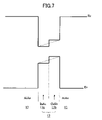
FIG. 7 is a diagram showing the band structure of the quantum dot of FIG. 6.
DETAILED DESCRIPTION OF THE INVENTION First Embodiment
FIG. 1 shows the construction of a single-photon generator 10 according to a first embodiment of the present invention.
Referring to FIG. 1, the single-photon generator 10 includes an undoped AlAs barrier layer 12 formed epitaxially on an n-type GaAs substrate 11 with a thickness of 20-30 nm, and quantum dots 13 of an InAs-GaSb system are formed with a large number on the AlAs barrier layer 12 with the S-K (Stranski-Krastanow) mode growth mechanism to be explained later.
As shown in FIG. 2, each of the quantum dots 13 has a compositional gradient therein, and thus has a compositional profile, such that the inside of the quantum dot is enriched with InAs and the outside of the quantum dot is enriched with GaSb.
Further, another undoped AlAs barrier layer 14 of about 20-30 nm in the thickness is formed epitaxially on the barrier layer 12 so as to bury the quantum dot 13, and a p-type GaAs contact layer 15 of about 20 nm thickness is formed epitaxially on the barrier layer 14.
On the contact layer, an upper electrode 16 having an optical window 16A in correspondence to one of the plural quantum dots 13 is provided in ohmic contact therewith, such that the optical window 16A is located immediately above the foregoing quantum dot, and a lower electrode 17 is formed on the bottom surface of the GaAs substrate 11 in ohmic contact therewith.
The single-photon generator 10 of FIG. 1 further includes a laser diode 18 having an oscillation wavelength of 800 nm-1 μm provided so as to illuminate the quantum dot 13, wherein the laser diode 18 causes excitation of excitons by emitting a laser beam 18A to the quantum dot 13 as will be explained with reference to FIG. 3A.
Further, the single-photon generator 10 of FIG. 1 includes a bias power supply 19 connected between the electrodes 16 and 17 through a switch circuit 19A, and a reverse bias voltage is applied to the electrodes 16 and 17 from the bias power supply 19 when the switch circuit 19A is closed under control of the control circuit 19B.
FIG. 3A shows the band diagram of the quantum dot 13 of FIG. 1 in an unbiased state.
Referring to FIG. 3A, an electron 1 and a hole 2 are excited in the quantum dot 13 when an excitation optical pulse having a wavelength ν corresponding to the bandgap of the quantum dot 13 comes in to the quantum dot 13. Because the conduction band Ec and the valence band Ev are inclined in the quantum dot 13 in correspondence to the compositional gradation explained previously, the electron thus excited is held in the lower end part of the quantum dot 13 enriched with InAs while the hole is held in the upper end part of the quantum dot 13 enriched with GaSb. Thereby, the electron and the hole are separated spatially as shown in the arrow in the drawing. Thus, the electron and hole are held in a polarized state and form an exciton. Because there is little overlapping of wavefunction between the electron and the hole, such an exciton is stable, and a recombination lifetime reaching 1.7-1.8 nanoseconds is achieved.
When the switch 19A is closed as shown in FIG. 3B, on the other hand, and a reverse bias voltage is applied between the electrode 16 and 17, and the band in the quantum dot 13 is flattened by the effect of the applied electric field. Thereby, the polarization or localization of the electron 1 and the hole 2 shown in FIG. 3A vanishes. In this case, an overlap is caused in the wavefunction of the electron and the wavefunction of the hole, and the electron 1 and the hole 2 cause recombination easily in the quantum dot 13. As a result of such a recombination, a single photon 3 is emitted.
The single photon thus formed exits through the optical window 16A in the electrode 16 as shown in FIG. 1 and is gated by an optical gate member 20 such as an acousto-optic device, which is controlled in synchronization with the switch circuit 19A by a control unit 19B. The single photon thus obtained is supplied to a quantum computer not illustrated.
In the excitation process that uses the laser 18 of FIG. 3A, there are cases in which plural electrons and holes are excited by the irradiation of the excitation optical beam, and thus, it is generally inevitable that there occurs formation of exciton molecules (exciton molecules) in addition to the exciton. In the case of such a exciton molecule, on the other hand, the degree of spatial separation of electron and hole is small as compared with the case of exciton shown in FIG. 3A, as schematically shown in FIG. 4, and thus, the electron and hole in the exciton molecule are annihilated efficiently in short time by causing recombination, typically within several hundred picoseconds, after the excitation. In the case of the exciton, the spatial separation between the electron and hole is large as explained before and a recombination lifetime of about 1.7-1.8 nanoseconds, which is longer than the recombination lifetime of a exciton molecule, is achieved.
Thus, in the single-photon generator 10 of FIG. 1, it becomes possible to produce only one single photon with reliability by constructing the control unit 19B such that the control unit 19B drives the switch 19A after the excitation by the laser beam 18A with the timing such that the recombination lifetime of exciton molecule has elapsed. For example, the control unit 19B drives the switch 19A after 1 nanosecond has elapsed after the excitation by the laser beam has been conducted. Thereby, the photons emitted by the recombination of the exciton molecules prior to the emission of the single photon are cut off successfully by synchronizing the optical gate member 20 with the switch circuit 19A.
For such an optical gate member 20, it is possible to use a high speed optical switching device that uses an electrooptic crystal such as KH2PO4, NH4H2PO4, LiNbO3, LiTaO3, and the like.
In the case the quantum dot 13 is formed by the S-K mode growth process, the distribution of the quantum dots 13 on the AlAs barrier layer 12 generally becomes random. Because the optical window 16A is formed in the electrode 16 in the single-photon generator 10 of FIG. 1 in correspondence to one of the plural quantum dots 13, the photon emission from other quantum dots are blocked by the electrode 16. In other words, the electrode 16 functions also as an optical mask in the single-photon generator 10 of FIG. 1.
FIGS. 5A-5D are diagrams explaining the operation of the single-photon generator 10 of FIG. 1.
Referring to FIGS. 5A and 5B, there occurs excitation of exciton or exciton molecules in correspondence to each optical pulse in the laser beam 18A produced by the laser diode 18 as shown in FIG. 5B, wherein the exciton molecules formed of plural electrons and holes are annihilated immediately as shown in FIG. 5B by a continuous line. On the other hand, the exciton formed of a single electron and a single hole has a long recombination lifetime and remains even after the exciton molecules have disappeared as shown in FIG. 5B by a broken line.
Thus, in the single-photon generator 10 of FIG. 1, the control unit 19B drives the switch 19A with the timing of FIG. 5C, and as a result, a single electron is emitted with the timing shown in FIG. 5C.
Further, by driving the optical gate member 20 with the timing of FIG. 5D in the single-photon generator 10 of FIG. 1, it becomes possible to take out only the necessary single photon for use in the external quantum computer, and the like.
Second Embodiment
Next, the method of forming the quantum dot 13 used with the construction of FIG. 1 will be explained briefly with reference to FIG. 6 as a second embodiment of the present invention.
Referring to FIG. 6, a GaAs substrate 11 formed with an AlAs layer 12 epitaxially thereon is introduced into an MBE apparatus and is held to a substrate temperature of 600° C. Further, an InAs layer 13 a is formed on the AlAs layer 12 with a thickness of 2-3 molecular layers by using molecular beams from an In cell and an As cell held to respective cell temperatures of 850° C. and 300° C. Because the InAs layer 13 a forms a strained system with respect to the GaAs substrate 11, the In atoms and the As atoms deposited on the AlAs layer 12 gather together on the surface, and there is formed an island or dot 13 a of InAs having a diameter is of about 20 nm.
In the present embodiment, a GaSb layer, forming a type II heterojunction to InAs, is formed on the InAs layer 13 a with the thickness of about 15 molecular layers, after the InAs dots 13 a are thus formed, by using the molecular beams from a Ga cell and a Sb cell held respectively to the cell temperatures of 950° C. and 480° C. In this case, because of the effect of the lattice strained system explained before, the Ga atoms and the Sb atoms concentrate on the InAs dot 13 a, and there is formed a GaSb layer 13 b on the InAs dot 13 a. It is known that such an InAs/GaSb dot forms a type II heterojunction in the case the diameter is smaller than 87 Å. (Phys. Rev. B. vol.48, 4643 (1993)).
FIG. 7 shows the band diagram of the structure of FIG. 6 thus formed.
Referring to FIG. 7, it can be seen that there is formed a heterojunction of type II between the InAs dot 13 a and the GaSb dot 13 b as shown in the continuous line in the drawing. Thereby, it is believed that there is formed a single dot having a compositional gradation as shown in the drawing by a broken line because of the mixing of elements caused between the GaSb dot 13 b and the InAs dot 13 a during the growth of the GaSb dot 13 b. Typically, such a dot has a diameter of about 20-50 nm and a height of about 5-10 nm and forms the quantum dot 13 in which the carriers are confined in three dimensions.
In the foregoing embodiment, the quantum dot 13 including therein the heterojunction of type II is not limited to the lamination of InAs and GaSb but it is also possible to use a lamination of InGaP and InP or GaAsSb and InP. Furthermore, the substrate 11 is not limited to GaAs but it is also possible to use an InP substrate or a GaP substrate, provided that it forms a strained system with regard to the quantum dot 13.
Further, the quantum dot 13 can be formed also by using an MOCVD process, in addition to the MBE process.
Further, the present invention is not limited to the embodiments described heretofore, but various variations and modifications may be made without departing from the scope of the invention.

Claims (20)

1. A single-photon generator, comprising:
an exciton generation part including therein a quantum dot having a band structure holding a single exciton;
an excitation part generating a plurality of excitons, including said single exciton, in said exciton generation part; and
a recombination control part controlling a recombination timing of said single exciton in said exciton generation part;
wherein said recombination control part, after generation of said plurality of excitons, causes recombination of the plurality of excitons excluding the single exciton in said exciton generation part, and subsequently changes said band structure to cause recombination of said single exciton in said exciton generation part.
2. The single-photon generator as claimed in claim 1, wherein said exciton generation part includes a type II heterojunction in said quantum dot.
3. The single-photon generator as claimed in claim 2, wherein said quantum dot changes a composition thereof from one side of said quantum dot to another side of said quantum dot continuously.
4. The single-photon generator as claimed in claim 1, wherein said quantum dot is formed of a quantum dot grown by a S-K mode growth process.
5. The single-photon generator as claimed in claim 1, wherein said quantum dot is formed of a lamination of an InAs layer and a GaSb layer sandwiched between a pair of AlAs layers, said InAs layer changing a composition thereof continuously toward said GaSb layer.
6. The single-photon generator as claimed in claim 1, wherein said recombination control part comprises an electrode provided in said exciton generation part, a voltage source applying a bias voltage to said electrode, and a switch circuit controlling application of said bias voltage from the voltage source to said electrode with a longer interval than a recombination lifetime of an exciton molecule, wherein the exciton molecule is excited simultaneously in the exciton generation part as said plurality of excitons.
7. The single-photon generator as claimed in claim 1, further comprising:
an optical gate member provided on a path of a single photon, the single photon is formed as a result of the recombination of said single exciton.
8. The single-photon generator as claimed in claim 7, wherein said optical gate member is controlled by said recombination control part and passes said single photon in synchronization with the recombination of said single exciton.
9. The single-photon generator as claimed in claim 1, wherein said excitation part comprises a laser.
10. The single-photon generator as claimed in claim 1, further comprising:
an optical window provided in said exciton generation part so as to pass a single photon formed as a result of the recombination of said single exciton.
11. The single-photon generator as claimed in claim 10, wherein said optical window is provided in said electrode.
12. A single-photon generating method, comprising:
forming, in a medium having a band structure holding a single exciton, a plurality of excitons including said single exciton;
causing recombination of the plurality of excitons excluding said single exciton in said medium; and
changing said band structure after said causing recombination to cause recombination of said single exciton in said medium.
13. The single-photon generating method as claimed in claim 12, wherein said causing recombination includes applying an electric field to said medium.
14. The single-photon generating method as claimed in claim 12, wherein said medium includes a quantum dot of type II heterojunction.
15. The single-photon generating method as claimed in claim 14, wherein said medium is formed of a quantum dot having a composition thereof, the composition being changed from one side of said quantum dot to the other side of said quantum dot continuously.
16. The single-photon generating method as claimed in claim 12, wherein said quantum dot is formed of a quantum dot grown by a S-K mode growth process.
17. The single-photon generating method as claimed in claim 12, wherein said quantum dot is formed of a lamination of an InAs layer and a GaSb layer sandwiched by a pair of AlAs layers, said InAs layer changing a composition thereof continuously toward said GaSb layer.
18. The single-photon generating method as claimed in claim 12, wherein said causing recombination controls a recombination timing of said single exciton in said medium by controlling an application of a bias voltage from a voltage source to an electrode which is provided with respect to said medium with a longer interval than a recombination lifetime of an exciton molecule excited simultaneously in said medium as said plurality of excitons.
19. The single-photon generating method as claimed in claim 12, wherein said causing recombination controls an optical gate member provided on a path of a single photon, which is formed as a result of the recombination of said single exciton, in synchronization with the recombination of said single exciton.
20. A single-photon generator, comprising:
an exciton generation part including therein a quantum dot;
an excitation part for generating an exciton in said exciton generation part;
a recombination control part for controlling recombination timing of said exciton in said exciton generation part; and
an optical window provided in said exciton generation part so as to pass a single photon formed as a result of recombination of said exciton,
said recombination control part causing, in said exciton generation part, recombination of said exciton at longer intervals than a recombination lifetime of an exciton molecule; and
wherein said quantum dot is formed of a lamination of an InAs layer and a GaSb layer sandwiched by a pair of AlAs layers, said InAs layer changing a composition thereof continuously toward said GaSb layer.
US10/779,816 2003-02-20 2004-02-18 Single-photon generator and single-photon generating method Expired - Fee Related US7492901B2 (en)

Applications Claiming Priority (2)

Application Number Priority Date Filing Date Title
JP2003043188A JP4360812B2 (en) 2003-02-20 2003-02-20 Single photon generator and single photon generation method
JP2003-043188 2003-02-20

Publications (2)

Publication Number Publication Date
US20040197070A1 US20040197070A1 (en) 2004-10-07
US7492901B2 true US7492901B2 (en) 2009-02-17

Family

ID=33026260

Family Applications (1)

Application Number Title Priority Date Filing Date
US10/779,816 Expired - Fee Related US7492901B2 (en) 2003-02-20 2004-02-18 Single-photon generator and single-photon generating method

Country Status (2)

Country Link
US (1) US7492901B2 (en)
JP (1) JP4360812B2 (en)

Cited By (3)

* Cited by examiner, † Cited by third party
Publication number Priority date Publication date Assignee Title
EP2592547A1 (en) 2011-11-09 2013-05-15 Novomatic AG Device for generating true random numbers and gaming system
RU2622228C1 (en) * 2016-08-23 2017-06-13 Федеральное государственное автономное образовательное учреждение высшего образования "Национальный исследовательский Нижегородский государственный университет им. Н.И. Лобачевского" Method of detection of the degree of influence of defect formation on the recombination time of carrier in semiconductor quantum points based on the heterojunction of the first type
US9697696B2 (en) 2011-09-26 2017-07-04 Novomatic Ag Gaming devices and methods of operating them

Families Citing this family (22)

* Cited by examiner, † Cited by third party
Publication number Priority date Publication date Assignee Title
US7465595B2 (en) * 2004-11-09 2008-12-16 Fujitsu Limited Quantum device, manufacturing method of the same and controlling method of the same
GB2440850B (en) * 2004-12-03 2008-08-20 Toshiba Res Europ Ltd Method of operating a photon source
GB2420908B (en) * 2004-12-03 2008-01-23 Toshiba Res Europ Ltd Photon source
WO2006095393A1 (en) * 2005-03-04 2006-09-14 Fujitsu Limited Optical semiconductor device and method for manufacturing same
JP4724035B2 (en) * 2006-03-30 2011-07-13 富士通株式会社 Single photon generator
JP5297519B2 (en) * 2006-05-15 2013-09-25 富士通株式会社 Manufacturing method of semiconductor device
JP5095260B2 (en) * 2006-05-15 2012-12-12 富士通株式会社 Manufacturing method of semiconductor light emitting device
TW200802941A (en) * 2006-06-22 2008-01-01 Univ Nat Central A quantum photoelectric element of antimony compound
JP5022753B2 (en) * 2007-03-29 2012-09-12 富士通株式会社 Cooling device for light emitting / receiving elements
JP5332886B2 (en) * 2008-07-14 2013-11-06 日本電気株式会社 Photon generator
JP5340684B2 (en) * 2008-09-24 2013-11-13 日本電信電話株式会社 Photon generator and method
JP5829375B2 (en) * 2009-06-05 2015-12-09 日本電気株式会社 OPTICAL ELEMENT AND PHOTON GENERATING DEVICE, LIGHT GENERATING DEVICE, OPTICAL RECORDING DEVICE AND OPTICAL DETECTING DEVICE USING THE SAME
GB2479162B (en) * 2010-03-30 2013-05-15 Toshiba Res Europ Ltd A quantum logic component and a method of controlling a qubit
JP6160995B2 (en) * 2013-07-31 2017-07-12 国立大学法人横浜国立大学 LIGHT EMITTING ELEMENT AND QUANTUM DEVICE USING THE SAME
GB2526140B (en) * 2014-05-15 2019-03-13 Toshiba Res Europe Limited Photon Source comprising a Control Signal and a Quantum Structure
JP6352081B2 (en) * 2014-07-07 2018-07-04 富士通株式会社 PHOTON GENERATION DEVICE, PHOTON GENERATION METHOD, AND CONTROL PROGRAM
US10320153B1 (en) * 2014-07-15 2019-06-11 Rudolf Heinrich Binder Systems and methods of an L-switched light emission
JP6350266B2 (en) * 2014-12-22 2018-07-04 富士通株式会社 Single photon generator and single photon generation method
CN109196397B (en) * 2016-09-06 2019-11-29 华为技术有限公司 For generating the device and system, fixed single-photon source method of single photon
GB201703594D0 (en) * 2017-03-07 2017-04-19 Univ Of Lancaster Single photon source
WO2020203746A1 (en) * 2019-04-02 2020-10-08 ローム株式会社 Single photon source and method for outputting single photon
WO2021047736A1 (en) * 2019-09-13 2021-03-18 Rheinisch-Westfälische Technische Hochschule (Rwth) Aachen Optically active quantum point defined by gates

Citations (3)

* Cited by examiner, † Cited by third party
Publication number Priority date Publication date Assignee Title
JP2001230445A (en) 2000-02-17 2001-08-24 Nec Corp Single-photon generation device
JP2002268104A (en) 2001-03-08 2002-09-18 Nippon Telegr & Teleph Corp <Ntt> Method and device for single photon generation
US20020196827A1 (en) * 2001-05-15 2002-12-26 Kabushhiki Kaisha Toshiba Photon source and a method of operating a photon source

Patent Citations (3)

* Cited by examiner, † Cited by third party
Publication number Priority date Publication date Assignee Title
JP2001230445A (en) 2000-02-17 2001-08-24 Nec Corp Single-photon generation device
JP2002268104A (en) 2001-03-08 2002-09-18 Nippon Telegr & Teleph Corp <Ntt> Method and device for single photon generation
US20020196827A1 (en) * 2001-05-15 2002-12-26 Kabushhiki Kaisha Toshiba Photon source and a method of operating a photon source

Non-Patent Citations (1)

* Cited by examiner, † Cited by third party
Title
Yamamoto, Y., et al, 'Single photons for quantum information systems', National Institute of Informatics, Dec. 6, 2004, entire document, http://www.nii.ac.jp/pi/n1/1-5.pdf. *

Cited By (6)

* Cited by examiner, † Cited by third party
Publication number Priority date Publication date Assignee Title
US9697696B2 (en) 2011-09-26 2017-07-04 Novomatic Ag Gaming devices and methods of operating them
EP2592547A1 (en) 2011-11-09 2013-05-15 Novomatic AG Device for generating true random numbers and gaming system
WO2013068546A1 (en) 2011-11-09 2013-05-16 Novomatic Ag Method of and device for generating true random numbers and a gaming system
CN103930866A (en) * 2011-11-09 2014-07-16 挪佛麦迪哥股份公司 Method of and device for generating true random numbers and a gaming system
US9747752B2 (en) 2011-11-09 2017-08-29 Novomatic Ag Method of and device for generating true random numbers and a gaming system
RU2622228C1 (en) * 2016-08-23 2017-06-13 Федеральное государственное автономное образовательное учреждение высшего образования "Национальный исследовательский Нижегородский государственный университет им. Н.И. Лобачевского" Method of detection of the degree of influence of defect formation on the recombination time of carrier in semiconductor quantum points based on the heterojunction of the first type

Also Published As

Publication number Publication date
JP4360812B2 (en) 2009-11-11
US20040197070A1 (en) 2004-10-07
JP2004253657A (en) 2004-09-09

Similar Documents

Publication Publication Date Title
US7492901B2 (en) Single-photon generator and single-photon generating method
Benson et al. Regulated and entangled photons from a single quantum dot
EP1503328B1 (en) Single-photon source
US6728281B1 (en) Quantum-dot photon turnstile device
Bimberg et al. Quantum dots for single-and entangled-photon emitters
WO2018193248A1 (en) A photonic device
ES2792076T3 (en) Monolithic device adjustable quantum light source and quantum optical circuit thereof
US7450718B2 (en) One-way synchronization of a two-way QKD system
Seidelmann et al. Two-photon excitation sets limit to entangled photon pair generation from quantum emitters
Müller et al. Active reset of a radiative cascade for entangled-photon generation beyond the continuous-driving limit
CN101040482A (en) Dual-gated qkd system for WDM networks
Ogura et al. Surface-emitting laser diode with distributed Bragg reflector and buried heterostructure
JP2001210860A (en) Optical device
JP4872302B2 (en) Single photon generator
JP3566365B2 (en) Optical semiconductor device
JP2758472B2 (en) Light modulator
Lochmann et al. Electrically driven quantum dot single photon source
JP2011141477A (en) Wavelength converting device and wavelength converting method
US6897993B2 (en) Electroabsorption modulator, modulator laser device and method for producing an electroabsorption modulator
JPH0632343B2 (en) Semiconductor laser
Stelmakh et al. Generation of high-energy (0.3/spl mu/J) short pulses (< 400 ps) from a gain-switched laser diode stack with subnanosecond electrical pump pulses
JPH0366188A (en) Multi-wavelength laser diode
JP2004516697A (en) Communication device
JP2680015B2 (en) Semiconductor laser device
Okuda et al. Quantum-confined field-effect light emitters: device physics and experiments

Legal Events

Date Code Title Description
AS Assignment

Owner name: FUJITSU LIMITED, JAPAN

Free format text: ASSIGNMENT OF ASSIGNORS INTEREST;ASSIGNORS:TAKEMOTO, KAZUYA;USUKI, TATSUYA;TAKATSU, MOTOMU;REEL/FRAME:014689/0244;SIGNING DATES FROM 20040216 TO 20040217

FEPP Fee payment procedure

Free format text: PAYOR NUMBER ASSIGNED (ORIGINAL EVENT CODE: ASPN); ENTITY STATUS OF PATENT OWNER: LARGE ENTITY

STCF Information on status: patent grant

Free format text: PATENTED CASE

FPAY Fee payment

Year of fee payment: 4

FPAY Fee payment

Year of fee payment: 8

FEPP Fee payment procedure

Free format text: MAINTENANCE FEE REMINDER MAILED (ORIGINAL EVENT CODE: REM.); ENTITY STATUS OF PATENT OWNER: LARGE ENTITY

LAPS Lapse for failure to pay maintenance fees

Free format text: PATENT EXPIRED FOR FAILURE TO PAY MAINTENANCE FEES (ORIGINAL EVENT CODE: EXP.); ENTITY STATUS OF PATENT OWNER: LARGE ENTITY

STCH Information on status: patent discontinuation

Free format text: PATENT EXPIRED DUE TO NONPAYMENT OF MAINTENANCE FEES UNDER 37 CFR 1.362

FP Lapsed due to failure to pay maintenance fee

Effective date: 20210217