US7428673B2 - Test method for determining the wire configuration for circuit carriers with components arranged thereon - Google Patents
Test method for determining the wire configuration for circuit carriers with components arranged thereon Download PDFInfo
- Publication number
- US7428673B2 US7428673B2 US11/214,482 US21448205A US7428673B2 US 7428673 B2 US7428673 B2 US 7428673B2 US 21448205 A US21448205 A US 21448205A US 7428673 B2 US7428673 B2 US 7428673B2
- Authority
- US
- United States
- Prior art keywords
- connections
- test
- memory
- memory module
- data
- Prior art date
- Legal status (The legal status is an assumption and is not a legal conclusion. Google has not performed a legal analysis and makes no representation as to the accuracy of the status listed.)
- Expired - Fee Related, expires
Links
Images


Classifications
-
- G—PHYSICS
- G11—INFORMATION STORAGE
- G11C—STATIC STORES
- G11C29/00—Checking stores for correct operation ; Subsequent repair; Testing stores during standby or offline operation
- G11C29/02—Detection or location of defective auxiliary circuits, e.g. defective refresh counters
-
- G—PHYSICS
- G11—INFORMATION STORAGE
- G11C—STATIC STORES
- G11C29/00—Checking stores for correct operation ; Subsequent repair; Testing stores during standby or offline operation
- G11C29/02—Detection or location of defective auxiliary circuits, e.g. defective refresh counters
- G11C29/025—Detection or location of defective auxiliary circuits, e.g. defective refresh counters in signal lines
-
- G—PHYSICS
- G11—INFORMATION STORAGE
- G11C—STATIC STORES
- G11C5/00—Details of stores covered by group G11C11/00
- G11C5/02—Disposition of storage elements, e.g. in the form of a matrix array
- G11C5/04—Supports for storage elements, e.g. memory modules; Mounting or fixing of storage elements on such supports
Definitions
- the invention relates to a test method for determining the wire configuration for a circuit carrier having at least one component arranged thereon, with connections of the component being wired to connections of the circuit carrier.
- the invention also relates to a memory module test system for carrying out the method on memory modules having memory chips arranged thereon.
- Circuit carriers such as circuit boards or modules, which can then be used flexibly, for example in PCs, and have standardized connections.
- memory modules having memory chips are known. Before memory modules are delivered, however, the functionality of the components or memory chips used needs to be checked by tests during production. Such memory tests involve address and data sequences being written and read by a memory tester, which allows errors to be identified within the chips. By way of example, electrical coupling between data or word lines is identified by writing appropriate data patterns and subsequently reading them using the memory tester.
- FIG. 1 shows an example of a memory chip 1 which has a memory cell array 2 with word and bit lines 3 , 4 .
- the bit lines or data lines 4 are driven by cell array amplifiers 5 .
- FIG. 1 shows four bit lines 4 - 1 , 4 - 2 , 4 - 3 , 4 - 4 , which are routed to connections 6 - 1 , 6 - 2 , 6 - 3 , 6 - 4 of the memory chip.
- bit lines or data lines are used for inputting and outputting data.
- the read/write access operations to such a memory chip are controlled by further control signals, which are input at further connections 7 , 8 , 9 of the memory chip 1 .
- the association between the data lines 4 and the data connections of the memory chips 6 - 1 , 6 - 2 , 6 - 3 , 6 - 4 is known. This is necessary in order to write particular test patterns to the memory cell array.
- FIG. 2 shows an example of a memory module 10 with four memory chips 11 , 12 , 13 , 14 which each have data connections 15 , 16 , 17 , 18 which are wired to data connections 19 , 20 , 21 , 22 of the memory module 10 .
- the exact wire configuration is unknown, which is shown by the blocks 23 , 24 , 25 , which are caused by unknown transposition or unknown scrambling of the wire configuration.
- the memory module For operation of the memory module, it is not necessary to have exact knowledge of the position of the data lines in the respective memory chips 11 , 12 , 13 , 14 , since the position of the memory cells is of no significance for storing and reading.
- the internal data lines of the memory chips 11 , 12 , 13 , 14 need to be a able to be actuated specifically, i.e. the wire configuration between the memory chip connections 15 , 16 , 17 , 18 and the module connections 19 , 20 , 21 , 22 needs to be known. This is because only then is it possible to apply appropriate test patterns for the memory cell arrays.
- test method for determining the wire configuration of circuit carriers having components arranged thereon which is particularly suitable for associating data connections of memory modules with appropriate internal data lines of memory chips arranged on the memory module.
- a test method for determining a wire configuration for a circuit carrier having at least one component arranged thereon is provided, where internal lines in the component are connected to component connections in a prescribed order, and where the component connections are wired to connections on the circuit carrier.
- the method includes the following method steps:
- test signal generator uses the internal lines of the component to deliver signals, inside the chip, to the connections of the component, which are routed to an external test apparatus via the component's wiring to the circuit carrier or the circuit carrier connections.
- This external test apparatus uses the known stipulations for the internally generated test signals to evaluate the corresponding output signals on the component connections and thus identifies a corresponding component connection for each circuit carrier connection, and hence the internal lines of the component, which may be data lines, for example.
- each component connection has an associated predetermined test signal level, and each output signal level tapped off from a circuit carrier connection which is the same as the test signal level is assigned a corresponding component connection.
- the component has first and second internal lines which are connected to first and second connections of the component in a prescribed order.
- the internal test signal generator is actuated for the purpose of applying internal test signals to the first internal lines using the second internal lines.
- the first and second connections of the component are wired to first and second connections of the circuit carrier.
- the component is a memory chip and the circuit carrier is a memory module.
- the first internal lines are data or bit lines associated with a word line.
- An external memory test apparatus is preferably coupled to the memory module via memory module connections and taps off the output signals, evaluates them and controls the internal test signal generator.
- the test signal generator is deactivated before the output signals are tapped off, and the tapping-off of the output signals by the memory test apparatus reads the test data which have been read in.
- the memory test apparatus determines the wire configuration by comparing the read data with the prescribed test data.
- test signal generators themselves are frequently provided in memory chips in order to check the functionality of the chip itself, this development is particularly suitable for also determining the wire configuration of the memory chip with the memory module.
- inventive combination of the internal test pattern or test data generation by the test signal generator and the reading of the data by an external memory test apparatus makes it a simple matter to associate the memory module connections with the internal data or bit lines of the chip.
- the method steps are repeated cyclically with different test data, each test cycle involving a first logic level being applied to a respective one of the internal data lines and a second logic level being applied to the remaining internal data lines.
- a respective external memory module connection is associated with each internal data line.
- a respective logic high level can be successively applied to each data line, i.e. per test cycle, which is equivalent to writing a bit, and subsequently read using the external memory test apparatus.
- a respective wire configuration between an internal data line and an external memory module connection is identified per test cycle.
- the test signal generator is an ACTM test pattern generator which can be programmed using the second internal lines.
- ACTM test pattern generators are already used for the memory chip test in DDR1 or DDR2 memory chips and can advantageously be programmed using address and control lines. In line with the invention, these test pattern generators are additionally used to detect the wire configuration of the memory modules.
- the invention also provides a test system for memory modules having:
- test data are advantageously stipulated or prescribed by programming the test signal generator during the actual production of the memory chip and are known to the external test apparatus.
- This has the advantage that standardized test data, for example a respective set bit for one of the data lines and otherwise unset bits, allow rapid evaluation of the output signals.
- the memory chip can be switched to a particular test mode via its control connections, which accept address and control signals, for example, by virtue of the test pattern generator generating control signals.
- the inventive idea of using the already available test pattern generator in the memory chip to write data to the memory cells in the chip but subsequently, in a reading step or the third test phase, to read these data externally using the memory test apparatus thus allows rapid and simple identification of the module data connections with the memory chip data connections.
- the ascertained wire configuration can advantageously be taken into account to perform a memory test on the memory cell array in the memory chip.
- the invention provides this very association and allows the specific actuation of, by way of example, adjacent bit or data lines in the memory chip.
- FIG. 1 shows a memory chip based on the prior art
- FIG. 2 shows a memory module based on the prior art
- FIG. 3 shows a block diagram of a memory module test system based on the invention.
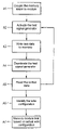
- FIG. 4 shows a flow chart of the inventive test method.
- FIG. 3 shows a test system or memory module test system 100 .
- a circuit carrier or memory module 101 has first connections 102 , 103 , 104 and second connections 105 , 106 , 107 .
- the first connections 102 , 103 , 104 are memory module data connections here and the second connections 105 , 106 , 107 are memory module control connections.
- the memory module 101 holds a component or memory chip 108 having first component connections or memory chip data connections 109 , 110 , 111 and second chip connections or memory chip control connections 112 , 113 , 114 .
- the memory chip connections 109 - 114 are wired to memory module connections 102 - 107 .
- Particularly the wire configuration between the memory module data connections 102 , 103 , 104 and the memory chip data connections 109 , 110 , 111 is frequently unknown on account of a lack of documentation for the memory module 101 .
- the memory chip 108 has a memory cell array 115 to which internal control and address lines 116 , 117 , 118 and internal data lines 119 , 120 , 121 are routed.
- the internal data lines 119 , 120 , 121 correspond to bit lines and the internal control and address lines 116 , 117 , 118 also correspond to word lines, for example.
- the memory cell array 115 has decoding devices and cell array amplifiers (not shown here) for actuating individual memory cells, as are known from the prior art.
- the memory chip has a controllable test signal generator 122 which is coupled to the internal data lines 119 , 120 , 121 and to the internal control lines 116 , 117 , 118 .
- the memory module 101 has a memory test apparatus 123 coupled to it which, for the purpose of carrying out the inventive test method, delivers control signals S 1 , S 2 , S 3 to first outputs 124 , 125 , 126 for the purpose of input to the module control connections 105 , 106 , 107 .
- the memory test apparatus 123 reads data D 1 , D 2 , D 3 from the memory module 101 or from the memory cell array 115 of the memory chip 108 .
- the connections 124 - 129 of the memory test apparatus 123 are in bidirectional form, in principle.
- the memory module 101 and the memory tester or memory test apparatus 123 are coupled to one another by means of lines (step A 1 ).
- the memory test apparatus 123 uses control signals S 1 , S 2 , S 3 to activate the test signal generator 122 in the first test phase A 2 .
- the internal test signal generator 122 writes prescribed test data E 1 , E 2 , E 3 to the memory cell array 115 of the memory chip 108 .
- the test pattern has been programmed into the test signal generator 122 at the start of the test mode, or else has been stipulated during the actual production of the memory chip 108 .
- step A 4 the memory test apparatus 122 uses appropriate control signals S 1 , S 2 , S 3 to deactivate the test signal generator 122 again.
- the data or test data E 1 , E 2 , E 3 which have been written remain in the memory cell array 115 of the memory chip 108 .
- a third test phase A 5 the memory tester 123 now uses address or control signals S 1 , S 2 , S 3 which have been input to the memory chip 108 to read the test data which have been written, in regular fashion.
- the second and third data lines 120 , 121 of the memory chip 108 are routed to the module data connections 103 , 104 the other way around by the wire configuration.
- This cycle A 2 -A 5 is repeated until the respective memory chip data connection 109 , 110 , 111 or the respective internal data line 119 , 120 , 121 can be associated with all module data connections 102 , 103 , 104 .
- step A 6 the complete wire configuration between module data connections 102 , 103 , 104 and memory chip data connections 109 , 110 , 111 is identified and determined.
- a fourth test phase A 7 the memory tester or the memory test apparatus 123 can correctly perform a memory test on the memory cell array 115 .
- the wire configuration it is also possible for, by way of example, adjacent memory cells associated with a word line to be actuated specifically and for memory tests to be used to check for coupling, for example.
- the invention's separate writing of test pattern data by the internal test signal generator 122 and separate reading of the written data by the memory test apparatus 123 thus allows reliable testing of memory modules 101 , even where there is insufficient documentation or an unknown wire configuration. This is possible, in particular, because the test signal sequence or the test patterns to be written can either be programmed into the test signal generator 122 by the memory test apparatus 123 itself or else is standardized and stipulated as defined during actual production.
Landscapes
- Tests Of Electronic Circuits (AREA)
Abstract
Description
- (a) a respective prescribed test signal is applied to each internal line of the component using a controllable test signal generator integrated in the component;
- (b) output signals applied to the connections of the circuit carrier are tapped off; and
- (c) the respective output signals tapped off are identified with the corresponding test signals applied to the internal lines of the component using an external test apparatus for determining the wire configuration between the component connections and circuit carrier connections.
- (i) the test signal generator is activated by means of control signals applied to the second connections of the circuit carrier,
- (ii) a respective prescribed internal test signal is applied to each of the first internal lines,
- (iii) the corresponding output signals are tapped off from the first connections of the circuit carrier, and
- (iv) the wire configuration between the first component connections and the first circuit carrier connections is determined by identifying the tapped-off output signals with the corresponding test signals applied to the first internal lines.
- (a) a memory module with external memory module connections;
- (b) at least one memory chip, arranged on the memory module, with memory chip data connections and memory chip control connections to which internal data lines and internal control lines in the memory chip are connected in a prescribed order, where the memory chip has an integrated controllable test signal generator which is connected to the internal memory chip data lines for the purpose of applying test signals and is connected to the internal control lines for the purpose of accepting and outputting control signals, the memory chip data connections being wired to module data connections and the memory chip control connections being wired to module control connections, and having
- (c) an external memory test apparatus, which is coupled to the module connections, for applying control signals to the module control connections and for tapping off output signals from the module data connections, where
- (d) in a first test phase the external memory test apparatus couples control signals for activating the test signal generator to the module control connections,
- (e) in a second test phase the internal test signal generator couples prescribed test signals to the memory chip data lines for the purpose of writing test data to the memory chip, and then the external memory test apparatus couples control signals for deactivating the test signal generator to the module control connections, and where
- (f) in a third test phase the memory test apparatus uses the module control connections and module data connections to read the written test data as output signals at the module data connections and compares the read data with the prescribed data written by the test signal generator in order to ascertain the wire configuration between the memory chip connections and the module data connections.
Claims (18)
Applications Claiming Priority (2)
| Application Number | Priority Date | Filing Date | Title |
|---|---|---|---|
| DE102004041553A DE102004041553B4 (en) | 2004-08-27 | 2004-08-27 | Test method for determining the wiring of circuit carriers with components arranged thereon |
| DE102004041553.6 | 2004-08-27 |
Publications (2)
| Publication Number | Publication Date |
|---|---|
| US20060053354A1 US20060053354A1 (en) | 2006-03-09 |
| US7428673B2 true US7428673B2 (en) | 2008-09-23 |
Family
ID=35997558
Family Applications (1)
| Application Number | Title | Priority Date | Filing Date |
|---|---|---|---|
| US11/214,482 Expired - Fee Related US7428673B2 (en) | 2004-08-27 | 2005-08-29 | Test method for determining the wire configuration for circuit carriers with components arranged thereon |
Country Status (2)
| Country | Link |
|---|---|
| US (1) | US7428673B2 (en) |
| DE (1) | DE102004041553B4 (en) |
Families Citing this family (1)
| Publication number | Priority date | Publication date | Assignee | Title |
|---|---|---|---|---|
| US9336387B2 (en) * | 2007-07-30 | 2016-05-10 | Stroz Friedberg, Inc. | System, method, and computer program product for detecting access to a memory device |
Citations (5)
| Publication number | Priority date | Publication date | Assignee | Title |
|---|---|---|---|---|
| DE10005161A1 (en) | 1999-04-30 | 2000-11-02 | Fujitsu Ltd | Semiconductor circuit with test function activated according to state of specific connection when supply switched on |
| US6345372B1 (en) | 1997-11-03 | 2002-02-05 | Infineon Technologies | Method for testing bus connections of writable and readable integrated electronic circuits, in particular memory components |
| DE10203570A1 (en) | 2002-01-30 | 2003-08-14 | Infineon Technologies Ag | Checking electrical connections between memory module and semiconducting component involves writing to memory with different address line biasing, reading and checking read item |
| US20040136249A1 (en) | 2002-12-12 | 2004-07-15 | Christian Stocken | Circuit arrangement having a number of integrated circuit components on a carrier substrate and method for testing a circuit arrangement of this type |
| US6925408B2 (en) * | 2003-09-08 | 2005-08-02 | Texas Instruments Incorporated | Mixed-signal core design for concurrent testing of mixed-signal, analog, and digital components |
Family Cites Families (1)
| Publication number | Priority date | Publication date | Assignee | Title |
|---|---|---|---|---|
| US6251796B1 (en) * | 2000-02-24 | 2001-06-26 | Conexant Systems, Inc. | Method for fabrication of ceramic tantalum nitride and improved structures based thereon |
-
2004
- 2004-08-27 DE DE102004041553A patent/DE102004041553B4/en not_active Expired - Fee Related
-
2005
- 2005-08-29 US US11/214,482 patent/US7428673B2/en not_active Expired - Fee Related
Patent Citations (9)
| Publication number | Priority date | Publication date | Assignee | Title |
|---|---|---|---|---|
| US6345372B1 (en) | 1997-11-03 | 2002-02-05 | Infineon Technologies | Method for testing bus connections of writable and readable integrated electronic circuits, in particular memory components |
| DE10005161A1 (en) | 1999-04-30 | 2000-11-02 | Fujitsu Ltd | Semiconductor circuit with test function activated according to state of specific connection when supply switched on |
| US6208571B1 (en) | 1999-04-30 | 2001-03-27 | Fujitsu Limited | Semiconductor memory device, circuit board mounted with semiconductor memory device, and method for testing interconnection between a semiconductor memory device with a circuit board |
| DE10203570A1 (en) | 2002-01-30 | 2003-08-14 | Infineon Technologies Ag | Checking electrical connections between memory module and semiconducting component involves writing to memory with different address line biasing, reading and checking read item |
| US20030169633A1 (en) | 2002-01-30 | 2003-09-11 | Frank Adler | Method of checking electrical connections between a memory module and a semiconductor memory chip |
| US6836440B2 (en) | 2002-01-30 | 2004-12-28 | Infineon Technologies Ag | Method of checking electrical connections between a memory module and a semiconductor memory chip |
| US20040136249A1 (en) | 2002-12-12 | 2004-07-15 | Christian Stocken | Circuit arrangement having a number of integrated circuit components on a carrier substrate and method for testing a circuit arrangement of this type |
| DE10258199A1 (en) | 2002-12-12 | 2004-07-15 | Infineon Technologies Ag | Circuit arrangement with a number of integrated circuit components on a carrier substrate and method for testing such a circuit arrangement |
| US6925408B2 (en) * | 2003-09-08 | 2005-08-02 | Texas Instruments Incorporated | Mixed-signal core design for concurrent testing of mixed-signal, analog, and digital components |
Non-Patent Citations (1)
| Title |
|---|
| Biewenga et al., "Static Component Interconnect Test Technology (SCITT), A New Technology for Assembly Testing", ITC International Test Conference, 1999, pp. 439-448, (10 pages). |
Also Published As
| Publication number | Publication date |
|---|---|
| DE102004041553A1 (en) | 2006-04-06 |
| DE102004041553B4 (en) | 2006-06-29 |
| US20060053354A1 (en) | 2006-03-09 |
Similar Documents
| Publication | Publication Date | Title |
|---|---|---|
| US6668347B1 (en) | Built-in self-testing for embedded memory | |
| US6883128B2 (en) | PC and ATE integrated chip test equipment | |
| US8020055B2 (en) | Method and apparatus for testing the connectivity of a flash memory chip | |
| JP2009003991A (en) | Semiconductor device and semiconductor memory test device | |
| WO2000052488A1 (en) | Distributed interface for parallel testing of multiple devices using a single tester channel | |
| US7904765B2 (en) | Test apparatus and test method | |
| EP3660526B1 (en) | Test system with embedded tester | |
| US8259484B2 (en) | 3D chip selection for shared input packages | |
| KR100541048B1 (en) | Semiconductor memory device and test method of the device | |
| US7428673B2 (en) | Test method for determining the wire configuration for circuit carriers with components arranged thereon | |
| JP2009099202A (en) | Semiconductor memory device | |
| US20050055618A1 (en) | Test arrangement and method for selecting a test mode output channel | |
| US20080028104A1 (en) | Semiconductor device and operation control method of semiconductor device | |
| US20060059397A1 (en) | Loop-back method for measuring the interface timing of semiconductor devices with the aid of signatures and/or parity methods | |
| JP4874391B2 (en) | Test equipment | |
| CN104952487B (en) | A method of operating a multi-chip packaging device | |
| CN100547424C (en) | Semiconductor device and method for testing semiconductor device | |
| US20050144525A1 (en) | Method to test memories that operate at twice their nominal bandwidth | |
| US20080316846A1 (en) | Semiconductor memory device capable of storing data of various patterns and method of electrically testing the semiconductor memory device | |
| US20070226591A1 (en) | Integrated device for simplified parallel testing, test board for testing a plurality of integrated devices, and test system and tester unit | |
| KR100868119B1 (en) | Integrated circuit, test system and method for reading out error data from said integrated circuit | |
| US6885961B2 (en) | Hybrid tester architecture | |
| US7461306B2 (en) | Output data compression scheme using tri-state | |
| CN100364010C (en) | A kind of EEPROM on-board programming method | |
| US7188291B2 (en) | Circuit and method for testing a circuit having memory array and addressing and control unit |
Legal Events
| Date | Code | Title | Description |
|---|---|---|---|
| AS | Assignment |
Owner name: INFINEON TECHNOLOGIES AG, GERMANY Free format text: ASSIGNMENT OF ASSIGNORS INTEREST;ASSIGNORS:KLIEWER, JORG;VERSEN, MARTIN;REEL/FRAME:017244/0957 Effective date: 20051010 |
|
| AS | Assignment |
Owner name: QIMONDA AG, GERMANY Free format text: ASSIGNMENT OF ASSIGNORS INTEREST;ASSIGNOR:INFINEON TECHNOLOGIES AG;REEL/FRAME:023806/0001 Effective date: 20060425 Owner name: QIMONDA AG,GERMANY Free format text: ASSIGNMENT OF ASSIGNORS INTEREST;ASSIGNOR:INFINEON TECHNOLOGIES AG;REEL/FRAME:023806/0001 Effective date: 20060425 |
|
| FPAY | Fee payment |
Year of fee payment: 4 |
|
| AS | Assignment |
Owner name: INFINEON TECHNOLOGIES AG, GERMANY Free format text: ASSIGNMENT OF ASSIGNORS INTEREST;ASSIGNOR:QIMONDA AG;REEL/FRAME:035623/0001 Effective date: 20141009 |
|
| AS | Assignment |
Owner name: POLARIS INNOVATIONS LIMITED, IRELAND Free format text: ASSIGNMENT OF ASSIGNORS INTEREST;ASSIGNOR:INFINEON TECHNOLOGIES AG;REEL/FRAME:036888/0745 Effective date: 20150708 |
|
| REMI | Maintenance fee reminder mailed | ||
| LAPS | Lapse for failure to pay maintenance fees | ||
| STCH | Information on status: patent discontinuation |
Free format text: PATENT EXPIRED DUE TO NONPAYMENT OF MAINTENANCE FEES UNDER 37 CFR 1.362 |
|
| STCH | Information on status: patent discontinuation |
Free format text: PATENT EXPIRED DUE TO NONPAYMENT OF MAINTENANCE FEES UNDER 37 CFR 1.362 |
|
| FP | Lapsed due to failure to pay maintenance fee |
Effective date: 20160923 |