US7403549B2 - Wavelength conversion laser and image display - Google Patents
Wavelength conversion laser and image display Download PDFInfo
- Publication number
- US7403549B2 US7403549B2 US10/554,248 US55424805A US7403549B2 US 7403549 B2 US7403549 B2 US 7403549B2 US 55424805 A US55424805 A US 55424805A US 7403549 B2 US7403549 B2 US 7403549B2
- Authority
- US
- United States
- Prior art keywords
- wavelength
- laser light
- laser
- light
- wavelength converter
- Prior art date
- Legal status (The legal status is an assumption and is not a legal conclusion. Google has not performed a legal analysis and makes no representation as to the accuracy of the status listed.)
- Expired - Lifetime, expires
Links
Images




Classifications
-
- H—ELECTRICITY
- H01—ELECTRIC ELEMENTS
- H01S—DEVICES USING THE PROCESS OF LIGHT AMPLIFICATION BY STIMULATED EMISSION OF RADIATION [LASER] TO AMPLIFY OR GENERATE LIGHT; DEVICES USING STIMULATED EMISSION OF ELECTROMAGNETIC RADIATION IN WAVE RANGES OTHER THAN OPTICAL
- H01S5/00—Semiconductor lasers
- H01S5/02—Structural details or components not essential to laser action
- H01S5/026—Monolithically integrated components, e.g. waveguides, monitoring photo-detectors, drivers
-
- G—PHYSICS
- G02—OPTICS
- G02F—OPTICAL DEVICES OR ARRANGEMENTS FOR THE CONTROL OF LIGHT BY MODIFICATION OF THE OPTICAL PROPERTIES OF THE MEDIA OF THE ELEMENTS INVOLVED THEREIN; NON-LINEAR OPTICS; FREQUENCY-CHANGING OF LIGHT; OPTICAL LOGIC ELEMENTS; OPTICAL ANALOGUE/DIGITAL CONVERTERS
- G02F1/00—Devices or arrangements for the control of the intensity, colour, phase, polarisation or direction of light arriving from an independent light source, e.g. switching, gating or modulating; Non-linear optics
- G02F1/35—Non-linear optics
- G02F1/37—Non-linear optics for second-harmonic generation
- G02F1/377—Non-linear optics for second-harmonic generation in an optical waveguide structure
- G02F1/3775—Non-linear optics for second-harmonic generation in an optical waveguide structure with a periodic structure, e.g. domain inversion, for quasi-phase-matching [QPM]
-
- H—ELECTRICITY
- H01—ELECTRIC ELEMENTS
- H01S—DEVICES USING THE PROCESS OF LIGHT AMPLIFICATION BY STIMULATED EMISSION OF RADIATION [LASER] TO AMPLIFY OR GENERATE LIGHT; DEVICES USING STIMULATED EMISSION OF ELECTROMAGNETIC RADIATION IN WAVE RANGES OTHER THAN OPTICAL
- H01S5/00—Semiconductor lasers
- H01S5/06—Arrangements for controlling the laser output parameters, e.g. by operating on the active medium
- H01S5/065—Mode locking; Mode suppression; Mode selection ; Self pulsating
-
- H—ELECTRICITY
- H01—ELECTRIC ELEMENTS
- H01S—DEVICES USING THE PROCESS OF LIGHT AMPLIFICATION BY STIMULATED EMISSION OF RADIATION [LASER] TO AMPLIFY OR GENERATE LIGHT; DEVICES USING STIMULATED EMISSION OF ELECTROMAGNETIC RADIATION IN WAVE RANGES OTHER THAN OPTICAL
- H01S5/00—Semiconductor lasers
- H01S5/10—Construction or shape of the optical resonator, e.g. extended or external cavity, coupled cavities, bent-guide, varying width, thickness or composition of the active region
- H01S5/1003—Waveguide having a modified shape along the axis, e.g. branched, curved, tapered, voids
- H01S5/1014—Tapered waveguide, e.g. spotsize converter
-
- H—ELECTRICITY
- H01—ELECTRIC ELEMENTS
- H01S—DEVICES USING THE PROCESS OF LIGHT AMPLIFICATION BY STIMULATED EMISSION OF RADIATION [LASER] TO AMPLIFY OR GENERATE LIGHT; DEVICES USING STIMULATED EMISSION OF ELECTROMAGNETIC RADIATION IN WAVE RANGES OTHER THAN OPTICAL
- H01S5/00—Semiconductor lasers
- H01S5/10—Construction or shape of the optical resonator, e.g. extended or external cavity, coupled cavities, bent-guide, varying width, thickness or composition of the active region
- H01S5/12—Construction or shape of the optical resonator, e.g. extended or external cavity, coupled cavities, bent-guide, varying width, thickness or composition of the active region the resonator having a periodic structure, e.g. in distributed feedback [DFB] lasers
-
- H—ELECTRICITY
- H01—ELECTRIC ELEMENTS
- H01S—DEVICES USING THE PROCESS OF LIGHT AMPLIFICATION BY STIMULATED EMISSION OF RADIATION [LASER] TO AMPLIFY OR GENERATE LIGHT; DEVICES USING STIMULATED EMISSION OF ELECTROMAGNETIC RADIATION IN WAVE RANGES OTHER THAN OPTICAL
- H01S5/00—Semiconductor lasers
- H01S5/10—Construction or shape of the optical resonator, e.g. extended or external cavity, coupled cavities, bent-guide, varying width, thickness or composition of the active region
- H01S5/14—External cavity lasers
- H01S5/141—External cavity lasers using a wavelength selective device, e.g. a grating or etalon
-
- G—PHYSICS
- G02—OPTICS
- G02F—OPTICAL DEVICES OR ARRANGEMENTS FOR THE CONTROL OF LIGHT BY MODIFICATION OF THE OPTICAL PROPERTIES OF THE MEDIA OF THE ELEMENTS INVOLVED THEREIN; NON-LINEAR OPTICS; FREQUENCY-CHANGING OF LIGHT; OPTICAL LOGIC ELEMENTS; OPTICAL ANALOGUE/DIGITAL CONVERTERS
- G02F2201/00—Constructional arrangements not provided for in groups G02F1/00 - G02F7/00
- G02F2201/34—Constructional arrangements not provided for in groups G02F1/00 - G02F7/00 reflector
-
- G—PHYSICS
- G02—OPTICS
- G02F—OPTICAL DEVICES OR ARRANGEMENTS FOR THE CONTROL OF LIGHT BY MODIFICATION OF THE OPTICAL PROPERTIES OF THE MEDIA OF THE ELEMENTS INVOLVED THEREIN; NON-LINEAR OPTICS; FREQUENCY-CHANGING OF LIGHT; OPTICAL LOGIC ELEMENTS; OPTICAL ANALOGUE/DIGITAL CONVERTERS
- G02F2201/00—Constructional arrangements not provided for in groups G02F1/00 - G02F7/00
- G02F2201/34—Constructional arrangements not provided for in groups G02F1/00 - G02F7/00 reflector
- G02F2201/346—Constructional arrangements not provided for in groups G02F1/00 - G02F7/00 reflector distributed (Bragg) reflector
-
- H—ELECTRICITY
- H01—ELECTRIC ELEMENTS
- H01S—DEVICES USING THE PROCESS OF LIGHT AMPLIFICATION BY STIMULATED EMISSION OF RADIATION [LASER] TO AMPLIFY OR GENERATE LIGHT; DEVICES USING STIMULATED EMISSION OF ELECTROMAGNETIC RADIATION IN WAVE RANGES OTHER THAN OPTICAL
- H01S3/00—Lasers, i.e. devices using stimulated emission of electromagnetic radiation in the infrared, visible or ultraviolet wave range
- H01S3/05—Construction or shape of optical resonators; Accommodation of active medium therein; Shape of active medium
- H01S3/08—Construction or shape of optical resonators or components thereof
- H01S3/08018—Mode suppression
- H01S3/0804—Transverse or lateral modes
- H01S3/08045—Single-mode emission
-
- H—ELECTRICITY
- H01—ELECTRIC ELEMENTS
- H01S—DEVICES USING THE PROCESS OF LIGHT AMPLIFICATION BY STIMULATED EMISSION OF RADIATION [LASER] TO AMPLIFY OR GENERATE LIGHT; DEVICES USING STIMULATED EMISSION OF ELECTROMAGNETIC RADIATION IN WAVE RANGES OTHER THAN OPTICAL
- H01S3/00—Lasers, i.e. devices using stimulated emission of electromagnetic radiation in the infrared, visible or ultraviolet wave range
- H01S3/05—Construction or shape of optical resonators; Accommodation of active medium therein; Shape of active medium
- H01S3/08—Construction or shape of optical resonators or components thereof
- H01S3/081—Construction or shape of optical resonators or components thereof comprising three or more reflectors
- H01S3/0813—Configuration of resonator
- H01S3/0815—Configuration of resonator having 3 reflectors, e.g. V-shaped resonators
-
- H—ELECTRICITY
- H01—ELECTRIC ELEMENTS
- H01S—DEVICES USING THE PROCESS OF LIGHT AMPLIFICATION BY STIMULATED EMISSION OF RADIATION [LASER] TO AMPLIFY OR GENERATE LIGHT; DEVICES USING STIMULATED EMISSION OF ELECTROMAGNETIC RADIATION IN WAVE RANGES OTHER THAN OPTICAL
- H01S3/00—Lasers, i.e. devices using stimulated emission of electromagnetic radiation in the infrared, visible or ultraviolet wave range
- H01S3/05—Construction or shape of optical resonators; Accommodation of active medium therein; Shape of active medium
- H01S3/08—Construction or shape of optical resonators or components thereof
- H01S3/081—Construction or shape of optical resonators or components thereof comprising three or more reflectors
- H01S3/082—Construction or shape of optical resonators or components thereof comprising three or more reflectors defining a plurality of resonators, e.g. for mode selection or suppression
-
- H—ELECTRICITY
- H01—ELECTRIC ELEMENTS
- H01S—DEVICES USING THE PROCESS OF LIGHT AMPLIFICATION BY STIMULATED EMISSION OF RADIATION [LASER] TO AMPLIFY OR GENERATE LIGHT; DEVICES USING STIMULATED EMISSION OF ELECTROMAGNETIC RADIATION IN WAVE RANGES OTHER THAN OPTICAL
- H01S3/00—Lasers, i.e. devices using stimulated emission of electromagnetic radiation in the infrared, visible or ultraviolet wave range
- H01S3/10—Controlling the intensity, frequency, phase, polarisation or direction of the emitted radiation, e.g. switching, gating, modulating or demodulating
- H01S3/106—Controlling the intensity, frequency, phase, polarisation or direction of the emitted radiation, e.g. switching, gating, modulating or demodulating by controlling devices placed within the cavity
- H01S3/108—Controlling the intensity, frequency, phase, polarisation or direction of the emitted radiation, e.g. switching, gating, modulating or demodulating by controlling devices placed within the cavity using non-linear optical devices, e.g. exhibiting Brillouin or Raman scattering
- H01S3/109—Frequency multiplication, e.g. harmonic generation
-
- H—ELECTRICITY
- H01—ELECTRIC ELEMENTS
- H01S—DEVICES USING THE PROCESS OF LIGHT AMPLIFICATION BY STIMULATED EMISSION OF RADIATION [LASER] TO AMPLIFY OR GENERATE LIGHT; DEVICES USING STIMULATED EMISSION OF ELECTROMAGNETIC RADIATION IN WAVE RANGES OTHER THAN OPTICAL
- H01S5/00—Semiconductor lasers
- H01S5/10—Construction or shape of the optical resonator, e.g. extended or external cavity, coupled cavities, bent-guide, varying width, thickness or composition of the active region
- H01S5/12—Construction or shape of the optical resonator, e.g. extended or external cavity, coupled cavities, bent-guide, varying width, thickness or composition of the active region the resonator having a periodic structure, e.g. in distributed feedback [DFB] lasers
- H01S5/125—Distributed Bragg reflector [DBR] lasers
-
- H—ELECTRICITY
- H01—ELECTRIC ELEMENTS
- H01S—DEVICES USING THE PROCESS OF LIGHT AMPLIFICATION BY STIMULATED EMISSION OF RADIATION [LASER] TO AMPLIFY OR GENERATE LIGHT; DEVICES USING STIMULATED EMISSION OF ELECTROMAGNETIC RADIATION IN WAVE RANGES OTHER THAN OPTICAL
- H01S5/00—Semiconductor lasers
- H01S5/10—Construction or shape of the optical resonator, e.g. extended or external cavity, coupled cavities, bent-guide, varying width, thickness or composition of the active region
- H01S5/14—External cavity lasers
-
- H—ELECTRICITY
- H01—ELECTRIC ELEMENTS
- H01S—DEVICES USING THE PROCESS OF LIGHT AMPLIFICATION BY STIMULATED EMISSION OF RADIATION [LASER] TO AMPLIFY OR GENERATE LIGHT; DEVICES USING STIMULATED EMISSION OF ELECTROMAGNETIC RADIATION IN WAVE RANGES OTHER THAN OPTICAL
- H01S5/00—Semiconductor lasers
- H01S5/20—Structure or shape of the semiconductor body to guide the optical wave ; Confining structures perpendicular to the optical axis, e.g. index or gain guiding, stripe geometry, broad area lasers, gain tailoring, transverse or lateral reflectors, special cladding structures, MQW barrier reflection layers
-
- H—ELECTRICITY
- H01—ELECTRIC ELEMENTS
- H01S—DEVICES USING THE PROCESS OF LIGHT AMPLIFICATION BY STIMULATED EMISSION OF RADIATION [LASER] TO AMPLIFY OR GENERATE LIGHT; DEVICES USING STIMULATED EMISSION OF ELECTROMAGNETIC RADIATION IN WAVE RANGES OTHER THAN OPTICAL
- H01S5/00—Semiconductor lasers
- H01S5/20—Structure or shape of the semiconductor body to guide the optical wave ; Confining structures perpendicular to the optical axis, e.g. index or gain guiding, stripe geometry, broad area lasers, gain tailoring, transverse or lateral reflectors, special cladding structures, MQW barrier reflection layers
- H01S5/2036—Broad area lasers
Definitions
- the present invention is related to a laser device and is especially related to wavelength conversion technology which can convert a laser to a short-wavelength laser.
- a wavelength converting laser device which converts near-infrared laser into short-wavelength laser by wavelength conversion is known.
- a wavelength converting laser device includes, a wavelength converter including a nonlinear optical material disposed either inside or outside of an optical resonator for a laser diode or a solid-state laser.
- a laser (a fundamental wave) generated by the optical resonator is output as a second harmonic wave which has a one-half the wavelength (double the frequency) of the fundamental wave as a result of propagation of the fundamental wave through the nonlinear optical material.
- this wavelength converting laser device includes a laser diode and a wavelength converter. It is impossible to produce a Watt-level laser (fundamental wave) with a narrow stripe semiconductor lasers having a small light emitting area.
- a mode control of a horizontal transverse mode horizontal to an active layer is not achieved in a broad-area laser diode having a large light emitting area and Watt-level power, that laser oscillates with multitude transverse modes and has low beam quality.
- this sort of broad-area laser diode it is impossible to obtain a highly efficient wavelength converting laser device since a laser (fundamental wave) with low beam quality has insufficient coupling efficiency or insufficient angle-turned phase matching with the wavelength converter.
- a wavelength converting laser device comprises a laser diode including an optical resonator having a pair of facing reflectors with a reflecting surface which reduces loss in optical resonator with regard to a specific horizontal transverse mode of a laser as compared to loss in optical resonator for other horizontal transverse modes and comprises a wavelength converter whereby the wavelength of the laser is converted into a harmonic.
- this wavelength converting laser device using a broad-area laser diode having a large light emitting area and Watt-level power output, oscillates with a high beam quality transverse mode through mode control of the horizontal transverse mode by the optical resonator. Therefore, the laser (fundamental wave) having Watt level power output as well as high beam quality achieves sufficient coupling efficiency or angle-turned phase matching with the wavelength converter and achieves highly efficient wavelength conversion.
- FIG. 1( a ) is a cross section parallel to vertical direction showing structure of a wavelength converting laser device in accordance with a first embodiment of the invention.
- FIG. 1( b ) is a cross section parallel to horizontal direction showing the structure of the wavelength converting laser device in accordance with the first embodiment of the invention.
- FIG. 2( a ) is a cross section parallel to vertical direction showing structure of the wavelength converting laser device in accordance with the first embodiment of the invention.
- FIG. 2( b ) is a cross section parallel to horizontal direction showing structure of the wavelength converting laser device in accordance with the first embodiment of the invention.
- FIG. 3( a ) is a cross section parallel to vertical direction showing structure of the wavelength converting laser device in accordance with a second embodiment of the invention.
- FIG. 3( b ) is a cross section parallel to horizontal direction showing structure of the wavelength converting laser device in accordance with the second embodiment of the invention.
- FIG. 4( a ) is a cross section parallel to vertical direction showing structure of the wavelength converting laser device in accordance with a third embodiment of the invention.
- FIG. 4( b ) is a cross section parallel to horizontal direction showing structure of the wavelength converting laser device in accordance with the third embodiment of the invention.
- FIG. 5( a ) is a cross section parallel to vertical direction showing structure of the wavelength converting laser device in accordance with the third embodiment of the invention.
- FIG. 5( b ) is a cross section parallel to horizontal direction showing structure of the wavelength converting laser device in accordance with the third embodiment of the invention.
- FIG. 6( a ) is a cross section parallel to vertical direction showing structure of the wavelength converting laser device in accordance with a fourth embodiment of the invention.
- FIG. 6( b ) is a cross section parallel to horizontal direction showing structure of the wavelength converting laser device in accordance with the fourth embodiment of the invention.
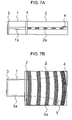
- FIG. 7( a ) is a cross section parallel to vertical direction showing structure of the wavelength converting laser device in accordance with a fifth embodiment of the invention.
- FIG. 7( b ) is a cross section parallel to horizontal direction showing structure of the wavelength converting laser device in accordance with the fifth embodiment of the invention.
- FIG. 8( a ) is a cross section parallel to vertical direction showing structure of the wavelength converting laser device in accordance with the fifth embodiment of the invention.
- FIG. 8( b ) is a cross section parallel to horizontal direction showing structure of the wavelength converting laser device in accordance with the fifth embodiment of the invention.
- FIG. 9( a ) is a cross section parallel to vertical direction showing structure of the wavelength converting laser device in accordance with a sixth embodiment of the invention.
- FIG. 9( b ) is a cross section parallel to horizontal direction showing structure of the wavelength converting laser device in accordance with the sixth embodiment of the invention.
- FIG. 10( a ) is a cross section parallel to vertical direction showing structure of the wavelength converting laser device in accordance with the sixth embodiment of the invention.
- FIG. 10( b ) is a cross section parallel to horizontal direction showing structure of the wavelength converting laser device in accordance with the sixth embodiment of the invention.
- FIG. 11( a ) is a cross section parallel to vertical direction showing structure of the wavelength converting laser device in accordance with the sixth embodiment of the invention.
- FIG. 11( b ) is a cross section parallel to horizontal direction showing structure of the wavelength converting laser device in accordance with the sixth embodiment of the invention.
- FIG. 12( a ) is a cross section parallel to vertical direction showing structure of the wavelength converting laser device in accordance with the sixth embodiment of the invention.
- FIG. 12( b ) is a cross section parallel to horizontal direction showing structure of the wavelength converting laser device in accordance with the sixth embodiment of the invention.
- FIG. 13( a ) is a cross section parallel to vertical direction showing structure of the wavelength converting laser device in accordance with a seventh embodiment of the invention.
- FIG. 13( b ) is a cross section parallel to horizontal direction showing structure of the wavelength converting laser device in accordance with the seventh embodiment of the invention.
- FIG. 14( a ) is a cross section parallel to vertical direction showing structure of the wavelength converting laser device in accordance with the seventh embodiment of the invention.
- FIG. 14( b ) is a cross section parallel to horizontal direction showing structure of the wavelength converting laser device in accordance with the seventh embodiment of the invention.
- FIG. 15( a ) is a cross section parallel to vertical direction showing structure of the wavelength converting laser device in accordance with an eighth embodiment of the invention.
- FIG. 15( b ) is a cross section parallel to horizontal direction showing structure of the wavelength converting laser device in accordance with the eighth embodiment of the invention.
- FIG. 16 is a block diagram showing structure of a display device in accordance with the ninth embodiment of the invention.
- a wavelength converting laser device in accordance with the first embodiment of this invention includes a laser diode and a wavelength converter disposed in an optical resonator.
- a laser (fundamental wave) oscillating within the optical resonator is output after wavelength conversion into a harmonic by the wavelength converter.
- Vertical transverse mode of the laser (fundamental wave) and the harmonic is controlled by an optical waveguide structure.
- the horizontal transverse mode of the laser (fundamental wave) and the harmonic is controlled by the optical resonator.
- FIG. 1 and FIG. 2 shows a structure of the wavelength converting laser device of the first embodiment of the invention.
- (a) illustrates a vertical cross-sectional view of the structure of the wavelength converting laser device perpendicular to an active layer of the laser diode
- (b) illustrates a horizontal cross-sectional view of the structure of the wavelength converting laser device horizontal to an active layer of the laser diode.
- the active layer 1 a made of, for example, an InGaAs-based compound semiconductor is formed in a laser diode 1 .
- the active layer 1 a has a thickness of about 1 ⁇ m and provides a slab waveguide which controls vertical transverse mode of a laser (fundamental wave).
- a pn junction is formed at boundaries of the active layer 1 a .
- the stripe width of the active layer is 200 ⁇ m, it is a so-called broad-area, and has a high power output characteristic with an output power of more than 5 Watts.
- the length of the laser diode 1 in the direction axis direction of the optical resonator is 4 mm and the laser diode 1 has a gain bandwidth of about 3 nm, centering around a wavelength of 946 nm.
- the wavelength converter 2 is made of, for example, MgO:LiNbO3 crystal having a periodically domain-inversed structure, and the z-axis of the crystal is aligned with a horizontal direction of the active layer 1 a .
- the wavelength converter 2 has a slab waveguide 2 a comparable in thickness to the thickness of the active layer 1 a of the laser diode 1 and having a wide width controlling the vertical transverse mode of the laser (fundamental wave) and a harmonic.
- length of the wavelength converter in the direction axis direction of the optical resonator is 10 mm.
- the periodically domain-inversed structure as illustrated by the striped pattern in the figures, has a domain-inversed period of 4.6 ⁇ m in the direction axis direction.
- the active layer 1 a of the laser diode 1 and the slab waveguide 2 a of the wavelength converter 2 are connected on their faces.
- the Reference number 3 indicates a first reflector
- reference number 4 indicates a second reflector. These reflectors are part of the optical resonator and the wavelength converter 2 is disposed within the optical resonator.
- the first reflector 3 is formed on a one facet of the laser diode 1 in an integrated structure and provides a coating which almost totally reflects light at a wavelength of 946 nm.
- the second reflector 4 is integrated with the wavelength converter 2 and is a distributed-reflectance-Bragg-grating-reflector (hereinafter called grating) which almost totally reflects light at a wavelength of 946 nm and has a high transmittance for light at a wavelength of 473 nm.
- the second reflector 4 has a 180 mm radius of curvature in the horizontal direction in order to control the horizontal transverse mode of the laser diode 1 .
- the first reflector 3 and the second reflector 4 have reflectance spectra with about 0.02 nm wavelength widths centered around a wavelength of 946 nm.
- the Reference number 5 illustrates simplified cross section parallel to horizontal direction of the fundamental wave beam traveling back and forth in the optical resonator.
- Laser oscillation occurs when amplification gain of the laser exceeds resonator loss, including absorption loss in the laser diode 1 , transmission loss in the first reflector 3 and the second reflector 4 , and losses due to the wavelength conversion and scattering in the wavelength converter.
- the vertical transverse mode of the laser (fundamental wave) is controlled by the active layer 1 a .
- the vertical transverse mode of the laser (fundamental wave) and the harmonic is controlled by the slab waveguide 2 a in the wavelength converter 2 .
- the horizontal transverse mode of the laser (fundamental wave) and the harmonic is not controlled by the active layer 1 a and the slab waveguide 2 a .
- the horizontal transverse mode of the laser (fundamental wave) is controlled by the first reflector 3 and the second reflector 4 which has the 180 nm radius of curvature.
- the spatial mode of the optical resonator is governed by the stripe width of the active layer and the radius of curvature of the second reflector 4 .
- the laser (fundamental wave) having a horizontal transverse mode with low loss in optical resonator oscillates and a wavefront of the laser (fundamental wave) at the second reflector 4 becomes almost parallel to the reflecting surface.
- the broad-area laser diode 1 has a high power output characteristic. It is possible to prevent optical damage and temperature rise at the wavelength converter 2 , from occurring by decreasing the power density of the laser (fundamental wave) by expanding the beam dimension in the horizontal direction. Thus, the harmonic can have a high-power. Both of the laser diode 1 and the wavelength converter 2 have an optical waveguide structure.
- wavelength conversion in the wavelength converter 2 is highly efficient by matching, in the vertical direction, waveguide mode of an optical waveguide comprising the laser diode 1 and the wavelength converter 2 , and by decreasing, in the horizontal direction, coupling loss of the laser (fundamental wave) traveling between the laser diode 1 and the wavelength converter 2 , as the spectral mode comprising the optical resonator including the pair of the reflectors.
- the power density of the laser (fundamental wave) and harmonic are reduced through expanding the beam dimension horizontally in the wavelength converter 2 . Therefore the heat generation caused by light absorption and temperature rising are prevented due to the enlarged heat releasing area.
- the wavelength converter 2 has the periodically domain-inversed structure, quasi-phase matching arises for the propagating harmonic, so it is possible to make the wavelength conversion in the wavelength converter 2 highly effective.
- phase velocity is different between the fundamental wave and the second harmonic wave and the second harmonic wave generated at each point propagates with a phase difference between each harmonic.
- the intensity of a synthesized harmonic decreases. Therefore, the intensity increases and decreases with a period of the coherence length.
- the wavelength of the fundamental wave is ⁇ 1
- the wavelength of the second harmonic wave is ⁇ 2
- refractive index of the nonlinear optical material at the fundamental wave is n 1
- refractive index at the second harmonic wave is n 2
- wave number vector of the fundamental wave k 1 (2 ⁇ n 1 / ⁇ 1 )
- wave number vector of the second harmonic wave k 2 (2 ⁇ n 2 / ⁇ 2 )
- phase of the second harmonic wave reverses in the period of coherence length and this becomes Quasi-Phase Matching compensating the phase of a synthesized harmonic and its intensity increases, in an additive manner, to generate the second harmonic wave efficiently.
- periodic pattern electrodes are formed on a substrate surface of the nonlinear optical material, so the polarization is inverted by applying a voltage exceeding the hold voltage of the ferroelectric material by the electric field application method. It is manufactured at interval of the coherence length, which is at a micron order, by applying the process technology for semiconductor.
- the polarization of the laser (fundamental wave) traveling back and force within the optical resonator is defined in the horizontal direction, it is possible to make the wavelength conversion in the wavelength converter highly efficient by aligning the z-axis of crystal axis having the greatest nonlinearity coefficient of the MgO:LiNbO3 crystal and the direction of polarization of the laser (fundamental wave).
- the interval of longitudinal modes of the laser depends on the length of the optical resonator and is 0.013 nm, which is sufficiently small.
- a longitudinal mode in the vicinity of wavelength 946 nm and within the wavelength width of the reflectance spectra of the first reflector 3 and the second reflector 4 is selected as a lasing wavelength of the laser (fundamental wave).
- the second reflector 4 includes the grating. Therefore, it is possible to make the wavelength conversion in the wavelength converter 2 highly efficient by reducing the phase mismatch of the harmonic by matching the phase matching wavelength of the wavelength converter 2 and the lasing wavelength of the laser (fundamental wave). Since the interval of the longitudinal modes is small enough, it is possible to control the lasing wavelength of the laser (fundamental wave) to be set sufficiently near the phase matching wavelength.
- the first reflector 3 and the second reflector 4 are integrated in the optical waveguide including the laser diode 1 and the wavelength converter 2 , diffraction loss of the laser (fundamental wave) traveling back and force within the optical resonator by reflecting toward the optical wave guide by the first reflector, 3 and the second reflector 4 can be reduced. Therefore it is possible to make the harmonic high power by the laser (fundamental wave) oscillating with high power.
- the laser (fundamental wave) is not output outside of the optical resonator and keeps confined within the optical resonator by the total reflection of the first reflector 3 and the second reflector 4 , only the wavelength-converted harmonic is output outside because of the high transmittance of the second reflector 4 . Since the wavelength converter is disposed inside the optical resonator within which the laser (fundamental wave) with high power is confined, the harmonic which is produced by wavelength conversion with high efficiency is output with high power.
- the wavelength of the laser (fundamental wave) with a wavelength of 946 nm is converted at high efficiency, the harmonic with a wavelength of 473 nm is output with high power of 3 Watt.
- the first reflector 3 is formed on the laser diode 1 in an integrated manner, as is the grating, which almost totally reflects light with a wavelength of 946 nm.
- the second reflector 4 is a coating integrated at the facet of wavelength converter 2 and almost totally reflects light at a wavelength of 946 nm and has a high transmittance for light at a wavelength of 473 nm.
- the coating representing the second reflector 4 is formed on the curved surface of the facet of the wavelength converter 2 , and has a radius of curvature of 180 nm in the horizontal direction in order to control the horizontal transverse mode of the laser (fundamental wave).
- the coating of the first reflector 3 and the grating of the second reflector 4 have reflectance spectra with about a 0.02 nm wavelength bandwidths centered around the wavelength of 946 nm in order to select a lasing wavelength.
- the structure as illustrated in FIG. 2 can also provide the same effect as the structure of FIG. 1 .
- the wavelength converting laser device in embodiment 1 of this invention makes it possible to produce oscillation with high quality transverse mode through the mode control of the horizontal transverse mode by the optical resonator. Therefore, since the laser (fundamental wave) having Watt level power output as well as high beam quality produces sufficient coupling efficiency, it is possible to achieve wavelength conversion with high efficiency. Further, it is possible to provide a wavelength converting laser device having Watt-level power output as well as high efficiency.
- a wavelength converting laser device in accordance with the second embodiment of this invention has almost the same structure and operation as the wavelength converting laser device of embodiment 1, but has a difference in an optical resonator.
- FIG. 3 shows a structure of the wavelength converting laser device in accordance with the second embodiment of this invention.
- (a) illustrates a vertical cross-sectional view of the structure of the wavelength converting laser device perpendicular to an active layer of the laser diode
- (b) illustrates a horizontal cross-sectional view of the structure of the wavelength converting laser device horizontal to an active layer of the laser diode.
- the same reference number indicates the same or a corresponding part in the Figures.
- the first reflector 3 is integrated with the laser diode 1 , and is a grating which almost totally reflects light at a wavelength of 946 nm.
- the second reflector 4 is integrated on a one facet of the wavelength converter 2 and is a coating which almost totally reflects light at a wavelength of 946 nm and has a high transmittance for light at a wavelength of 473 nm.
- the grating of the first reflector 3 has a 170 mm radius of curvature in the horizontal direction in order to control the horizontal transverse mode.
- the vertical transverse mode of the laser (fundamental wave) is controlled by an optical waveguide structure including a laser diode 1 and a wavelength converter 2 .
- the horizontal transverse mode of the laser (fundamental wave) is controlled by the first reflector 3 having a 170 mm radius of curvature and the second reflector 4 .
- the spatial mode of the optical resonator is governed by the stripe width of the active layer and the radius of curvature of the first reflector 3 .
- the laser (fundamental wave) having a horizontal transverse mode with low loss in optical resonator oscillates and a wavefront of the laser (fundamental wave) at the first reflector 3 becomes almost parallel to the reflecting surface.
- the first reflector 3 may be a coating having a 170 mm radius of curvature and the second reflector 4 may be a grating.
- a wavelength converting laser device in accordance with the third embodiment of this invention has almost the same structure and operation as the wavelength converting laser device of embodiment 1 and embodiment 2, but has an adjustment means for adjusting a angle-turned phase matching in the wavelength converter.
- FIG. 4 and FIG. 5 show a structure of the wavelength converting laser device in accordance with the third embodiment of this invention.
- (a) illustrates a vertical cross-sectional view of the structure of the wavelength converting laser device perpendicular to the active layer of the laser diode
- (b) illustrates a horizontal cross-sectional view of the structure of the wavelength converting laser device horizontal to the active layer of the laser diode.
- the same reference number indicates the same or a corresponding part in the figures.
- the laser diode 1 is a broad-area diode having a stripe width of active layer of 100 ⁇ m and has a high power output characteristic.
- the grating as the second reflector 4 has a 16 mm radius of curvature in the horizontal direction in order to control the horizontal transverse mode.
- the periodically domain-inversed structure of the wavelength converter 2 has a domain-inversed period of about 4.6 ⁇ m and is formed into curved surface shape, almost parallel to a wavefront of the laser (fundamental wave) in the horizontal direction, in order to adjust the angle-turned phase matching.
- a problem of the angle-turned phase matching is that an allowable value of a propagation angle is restricted when the harmonic is performed phase matching and the fundamental wave travels back and forth within the wavelength converter. Therefore, it is necessary to achieve the laser as the fundamental wave having a nice beam quality with a small beam expansion.
- the beam of the fundamental wave expands in a curved surface manner.
- the domain-inversed period ⁇ changes into ⁇ /cos ⁇ , and this decreases conversion efficiency in the surrounding portion of the beam.
- the beam of the laser expands in the horizontal direction and inclines by up to 0.1 deg.
- the periodically domain-inversed structure is formed into the curved surface shape so as to be almost parallel to the wavefront of the laser (fundamental wave) in the horizontal direction, the domain-inversed period almost matches the expansion of the beam of the fundamental wave and the harmonic receives a sufficient quasi-phase matching.
- the laser diode 1 is a broad-area having a stripe width of active layer of 120 ⁇ m and has a high power output characteristic.
- the grating as the second reflector 4 has a 14 mm radius of curvature in the horizontal direction in order to control the horizontal transverse mode.
- the periodically domain-inversed structure of the wavelength converter 2 has a domain-inversed period of 4.6 ⁇ m and is formed into curved surface shape, almost parallel to the wavefront of the laser (fundamental wave) in the horizontal direction, in order to adjust the angle-turned phase matching.
- the beam of the laser (fundamental wave) expands in the horizontal direction and inclines by up to 0.06 deg.
- the beam of the laser (fundamental wave) expands in the horizontal direction and inclines by up to 0.06 deg.
- the periodically domain-inversed structure is formed into curved surface shape, almost parallel to the wavefront of the laser (fundamental wave), in order to adjust the angle-turned phase matching, it is possible to make the quasi-phase matching sufficient and to achieve the highlly efficient wavelength conversion.
- a wavelength converting laser device in accordance with the fourth embodiment of the invention has almost the same structure and operation as the wavelength converting laser device of embodiment 3, but includes an optical waveguide device on which a reflector of an optical resonator is formed.
- FIG. 6 shows a structure of the wavelength converting laser device in accordance with the fourth embodiment of this invention.
- (a) illustrates a vertical cross-sectional view of the structure of the wavelength converting laser device perpendicular to the active layer of the laser diode
- (b) illustrates a horizontal cross-sectional view of the structure of the wavelength converting laser device horizontal to the active layer of the laser diode.
- the same reference number indicates the same or a corresponding part in the figures.
- reference number 6 indicates the optical waveguide device including a slab waveguide 6 a having the almost same thickness as that of the slab waveguide 2 a of the wavelength converter 2 .
- the wavelength converter has a length of 5 mm
- the second reflector 4 is a grating integrated on the optical waveguide device and has a 130 mm radius of curvature in the horizontal direction.
- the first reflector 3 is a grating integrated on an optical waveguide device which includes a slab waveguide having almost the same thickness as that of the active layer 1 a of the laser diode 1 . It is possible to achieve the same effects.
- a wavelength converting laser device in accordance with the fifth embodiment of the invention has almost the same structure and operation as the wavelength converting laser device of embodiment 3, but includes a reflector configured to reflect the harmonic between the laser diode and the wavelength converter.
- FIG. 7 and FIG. 8 show a structure of the wavelength converting laser device in accordance with the fifth embodiment of this invention.
- (a) illustrates a vertical cross-sectional view of the structure of the wavelength converting laser device perpendicular to the active layer of the laser diode
- (b) illustrates a horizontal cross-sectional view of the structure of the wavelength converting laser device horizontal to the active layer of the laser diode.
- the same reference number indicates the same or a corresponding part in the figures.
- the reference number 7 indicates a third reflector which is placed between the laser diode 1 and-the wavelength converter 2 and which is a coating that almost totally reflects light at a wavelength of 473 nm.
- the third reflector 7 is formed on an optical waveguide device 6 disposed between the laser diode 1 and the wavelength converter 2 and is a grating that almost totally reflects light at a wavelength of 473 nm.
- the wavelength converter 2 is disposed within the optical resonator, since the laser (fundamental wave) travels back and forth within the optical resonator, the wavelength of the laser propagating towards the direction of the laser diode 1 from the wavelength converter 2 is also converted to the harmonic by the wavelength converter 2 . Therefore, it is possible to make producing of the harmonic more highly efficient through reflecting the laser propagating towards the direction of the laser diode 1 from the wavelength converter 2 by the third reflector 7 and outputting them from the second reflector. Furthermore, it is possible to prevent optical damage and temperature rise, caused by absorption of the harmonic in the active layer 1 a of the laser diode 1 , from occurring, by blocking the incidence of the harmonic into the laser diode 1 by the third reflector 7 .
- a wavelength converting laser device in accordance with the sixth embodiment of the invention has almost the same structure and operation as the wavelength converting laser device of embodiment 5, but includes a vertical transverse mode converting means between the laser diode and the wavelength converter.
- FIG. 9 , FIG. 10 , FIG. 11 and FIG. 12 show a structure of the wavelength converting laser device in accordance with the sixth embodiment of this invention.
- (a) illustrates a vertical cross-sectional view of the structure of the wavelength converting laser device perpendicular to the active layer of the laser diode
- (b) illustrates a horizontal cross-sectional view of the structure of the wavelength converting laser device horizontal to the active layer of the laser diode.
- the same reference number indicates the same or a corresponding part in the figures.
- the thickness of the slab waveguide of the laser diode 1 is different than that of the slab waveguide of the wavelength converter.
- the reference number 8 estimates transverse mode converting means in which a thickness of a slab waveguide formed on an optical waveguide changes gradually.
- the wavelength converting laser device includes, as the transverse mode converting means 8 , a cylindrical lens having a curved surface only in the vertical direction.
- the wavelength converting laser device includes, as the transverse mode converting means 8 , a graded-index-type lens having a distribution of the refractive index under which the reflection gradually decreases in the vertical direction.
- a thickness of the active layer 1 a of the laser diode 1 changes gradually as the transverse mode converting means 8 .
- the thickness and distribution of the refractive index of the slab waveguide are different between the laser diode 1 and the wavelength converter 2 , a mode mismatching between the vertical transverse mode of the laser in the laser diode 1 and the vertical transverse mode of the laser in the wavelength converter 2 occurs.
- a wavelength converting laser device in accordance with the seventh embodiment of the invention has almost the same structure and operation as the wavelength converting laser device of embodiment 5, but includes a temperature control means for the laser diode and the wavelength converter.
- FIG. 13 and FIG. 14 show a structure of the wavelength converting laser device in accordance with the seventh embodiment of this invention.
- (a) illustrates a vertical cross-sectional view of the structure of the wavelength converting laser device perpendicular to the active layer of the laser diode
- (b) illustrates a horizontal cross-sectional view of the structure of the wavelength converting laser device horizontal to the active layer of the laser diode.
- the same reference number indicates the same or a corresponding part in the figures.
- reference number 9 indicates a temperature control means disposed to come into contact with the wavelength converter 2 and being a peltier device (thermoelectric device) changing and maintaining the temperature of the wavelength converter 2 .
- a phase matching wavelength causes wavelength-shift due to a change of the refractive index and thermal expansion.
- the temperature of the second reflector 4 integrated with the wavelength converter 2 changes also and the reflectance spectrum cause wavelength-shift due to the change of refractive index of the grating and the thermal expansion.
- a lasing wavelength of the laser (fundamental wave) depending on this reflectance spectrum causes wavelength-shift.
- the ratio of the wavelength-shift to the temperature change is different between the phase matching wavelength and the lasing wavelength, it is possible to adjust them so as to almost much the phase matching wavelength with the lasing wavelength by controlling the temperature of the wavelength converter 2 .
- the temperature control means 9 is a peltier device (thermoelectric device) disposed so as to come into contact with the laser diode 1 , wavelength converter 2 , and the optical waveguide device 6 , which changes and maintains the temperature of them.
- the ratio of the wavelength-shift to the temperature change at the phase matching wavelength is configured to be almost the same as that at the lasing wavelength, the conversion efficiency is kept almost constant without temperature control. Therefore, it is possible, for the structure as illustrated in FIG. 14 , to counterbalance the change of refractive index due to the temperature change and influence by the thermal expansion of each element by selecting a suitable material for the optical waveguide device 6 . Therefore, even if ambient temperature changes, it is possible to reduce the phase mismatching amount of the harmonic by matching the phase matching wavelength of the wavelength converter 2 with the lasing wavelength of the laser (fundamental wave) without the temperature control, and is possible to make the wavelength conversion in the wavelength converter 2 highly efficient.
- a wavelength converting laser device in accordance with the eighth embodiment of this invention includes a wavelength converter disposed outside of the laser diode and the optical resonator.
- a laser (fundamental wave) oscillating within the optical resonator is output after wavelength conversion into a harmonic by the wavelength converter.
- Vertical transverse mode of the laser (fundamental wave) and of the harmonic is controlled by an optical waveguide structure.
- the horizontal transverse mode of the laser (fundamental wave) is controlled by the optical resonator.
- FIG. 15 shows a structure of the wavelength converting laser device of the eighth embodiment of the invention.
- (a) illustrates a vertical cross-sectional view of the structure of the wavelength converting laser device perpendicular to an active layer of the laser diode
- (b) illustrates a horizontal cross-sectional view of the structure of the wavelength converting laser device horizontal to an active layer of the laser diode.
- the same reference number indicates the same or a corresponding part in the Figures.
- the first reflector 3 is formed on a one facet of the laser diode 1 in an integrated structure and provides a coating which almost totally reflects light at a wavelength of 946 nm.
- the second reflector 4 is integrated with the laser diode 1 and is a grating which partially reflects light at a wavelength of 946 nm.
- the grating of the second reflector 4 has a radius of curvature in the horizontal direction in order to control the horizontal transverse mode.
- the wavelength converter 2 is disposed outside of the optical resonator keeping in touch with a one facet of the laser diode 1 .
- laser oscillation occurs when amplification gain of the laser exceeds resonator loss, including absorption in the laser diode 1 and transmission loss in the first reflector 3 and the second reflector 4 .
- the vertical transverse mode of the laser (fundamental wave) is controlled by the active layer 1 a .
- the vertical transverse mode of the laser (fundamental wave) and of the harmonic is controlled by the slab waveguide 2 a .
- the horizontal transverse mode of the laser (fundamental wave) and of the harmonic is not controlled by the active layer 1 a and the slab waveguide 2 a .
- the horizontal transverse mode of the laser (fundamental wave) is controlled by the first reflector 3 and the second reflector 4 which has the radius of curvature.
- the spatial mode of the optical resonator is governed by the radius of curvature of the second reflector 4 .
- the laser (fundamental wave) having a horizontal transverse mode with low loss in optical resonator oscillates and a wavefront of the laser (fundamental wave) at the second reflector 4 becomes almost parallel to the reflecting surface.
- the broad-area laser diode 1 has a high power output characteristic. It is possible to prevent optical damage and temperature rise at the wavelength converter 2 from occurring by decreasing the power density of the laser (fundamental wave) by expanding the beam dimension in the horizontal direction. Thus, the harmonic can have a high-power.
- Both of the laser diode 1 and the wavelength converter 2 have an optical waveguide structure.
- wavelength conversion in the wavelength converter 2 is highly efficient by matching, in the vertical direction, the waveguide mode of the optical waveguide comprising the laser diode 1 and the wavelength converter 2 , and by decreasing, in the horizontal direction, coupling loss of the laser (fundamental wave) traveling between the laser diode 1 and the wavelength converter 2 , as the spectral mode comprising the optical resonator including the pair of the reflectors.
- the laser (fundamental wave) traveling back and forth within the optical resonator its polarization is defined in the horizontal direction. Therefore, it is possible to make the wavelength conversion in the wavelength converter highly efficient by aligning the z-axis of crystal axis having the greatest nonlinear coefficient of wavelength converter 2 with the direction of polarization of the laser (fundamental wave).
- the wavelength converter 2 has the periodically domain-inversed structure, quasi-phase matching arises for the propagating harmonic, so it is possible to make the wavelength conversion in the wavelength converter 2 highly efficient.
- the periodically domain-inversed structure is formed, along with a direction which the beam propagates, to be almost parallel to the wavefront of the laser (fundamental wave) in the horizontal direction. Thus, since this makes the angle-turned phase matching sufficient, it is possible to make the wavelength conversion in the wavelength converter 2 highly efficient.
- the interval of the longitudinal mode of the laser depends on length of the optical resonator and is 0.13 nm.
- a lasing wavelength of the laser As a lasing wavelength of the laser, a longitudinal mode, around the wavelength of 946 nm, within the wavelength bandwidths of reflectance spectra of the first reflector 3 and the second reflector 4 is selected.
- the second reflector 4 includes the grating. Therefore, it is possible to make the wavelength conversion in the wavelength converter 2 highly efficient by reducing the phase mismatch of the harmonic by matching the phase matching wavelength of the wavelength converter 2 and the lasing wavelength of the laser (fundamental wave).
- a display device in accordance with the ninth embodiment of this invention uses any one of the wavelength converting laser device in accordance with embodiments 1-8 as a light source 10 to generate images.
- the display device of this invention modulates a laser from a high-intensity light source 10 by an optical modulating means 14 and projects them to generate images on a screen 15 .
- a wavelength converting laser device 11 having a 3 Watt power output at a wavelength of 473 nm is used for a blue light source and a wavelength converting laser device 12 having a 2 Watt power output at a wavelength of 532 nm is used for a green light source.
- laser diode device 13 is used.
- a liquid crystal or a digital reflecting element DMD Digital Micro-minor Device
- a liquid crystal display device using the liquid crystal as the optical modulating means 14 an element is made by holding a liquid crystal material between, for example, glass substrates and images are generated by utilizing the change of optical property of the element, caused with change of the molecular arrangement of the liquid crystal, caused by applying an external electric field.
- images are generated by arranging, in two-dimensions, micro-mirrors produced by MEMS technology (Micro Electro Mechanical Systems) and by on-off driving through swinging each mirror.
- MEMS technology Micro Electro Mechanical Systems
- the wavelength converting laser device When the wavelength converting laser device is used as a light source for generating images, since it has an advantage of monochromatic output and high intensity of the laser compared with conventional lamp apparatuses, it is possible to improve the usability of light energy in generation of images by the optical modulating means. Besides, since the wavelength converting laser device has an advantage such as higher efficiency and longer operating life compared with conventional lamp apparatuses, it is possible to make the display device energy conserving and have a longer operating time.
Landscapes
- Physics & Mathematics (AREA)
- General Physics & Mathematics (AREA)
- Optics & Photonics (AREA)
- Condensed Matter Physics & Semiconductors (AREA)
- Electromagnetism (AREA)
- Nonlinear Science (AREA)
- Optical Modulation, Optical Deflection, Nonlinear Optics, Optical Demodulation, Optical Logic Elements (AREA)
- Semiconductor Lasers (AREA)
- Lasers (AREA)
Priority Applications (1)
| Application Number | Priority Date | Filing Date | Title |
|---|---|---|---|
| US12/107,105 US7778291B2 (en) | 2003-10-01 | 2008-04-22 | Wavelength converting laser device |
Applications Claiming Priority (1)
| Application Number | Priority Date | Filing Date | Title |
|---|---|---|---|
| PCT/JP2003/012601 WO2005033791A1 (ja) | 2003-10-01 | 2003-10-01 | 波長変換レーザ装置および画像表示装置 |
Related Child Applications (1)
| Application Number | Title | Priority Date | Filing Date |
|---|---|---|---|
| US12/107,105 Continuation US7778291B2 (en) | 2003-10-01 | 2008-04-22 | Wavelength converting laser device |
Publications (2)
| Publication Number | Publication Date |
|---|---|
| US20060256829A1 US20060256829A1 (en) | 2006-11-16 |
| US7403549B2 true US7403549B2 (en) | 2008-07-22 |
Family
ID=34401445
Family Applications (2)
| Application Number | Title | Priority Date | Filing Date |
|---|---|---|---|
| US10/554,248 Expired - Lifetime US7403549B2 (en) | 2003-10-01 | 2003-10-01 | Wavelength conversion laser and image display |
| US12/107,105 Expired - Fee Related US7778291B2 (en) | 2003-10-01 | 2008-04-22 | Wavelength converting laser device |
Family Applications After (1)
| Application Number | Title | Priority Date | Filing Date |
|---|---|---|---|
| US12/107,105 Expired - Fee Related US7778291B2 (en) | 2003-10-01 | 2008-04-22 | Wavelength converting laser device |
Country Status (4)
| Country | Link |
|---|---|
| US (2) | US7403549B2 (de) |
| EP (1) | EP1669799B1 (de) |
| JP (1) | JP4747841B2 (de) |
| WO (1) | WO2005033791A1 (de) |
Cited By (3)
| Publication number | Priority date | Publication date | Assignee | Title |
|---|---|---|---|---|
| US20050238071A1 (en) * | 2004-04-22 | 2005-10-27 | Michio Oka | One-dimensional illumination apparatus and imaging apparatus |
| US20100303112A1 (en) * | 2007-08-30 | 2010-12-02 | Mitsubishi Electric Corporation | Solid-state laser element |
| US8149887B2 (en) | 2007-07-27 | 2012-04-03 | Mitsubishi Electric Corporation | Planar waveguide laser device |
Families Citing this family (19)
| Publication number | Priority date | Publication date | Assignee | Title |
|---|---|---|---|---|
| EP1669799B1 (de) * | 2003-10-01 | 2013-06-19 | Mitsubishi Denki Kabushiki Kaisha | Wellenlängenumsetzungslaser und bildanzeige |
| US20060165137A1 (en) * | 2005-01-21 | 2006-07-27 | Alexander Kachanov | Novel external cavity CW frequency doubling of semiconductor lasers to generate 300-600nm light |
| WO2006103767A1 (ja) | 2005-03-30 | 2006-10-05 | Mitsubishi Denki Kabushiki Kaisha | モード制御導波路型レーザ装置 |
| CN101253659B (zh) * | 2005-08-29 | 2010-12-29 | 松下电器产业株式会社 | 光纤激光器及光学装置 |
| WO2009016709A1 (ja) * | 2007-07-30 | 2009-02-05 | Mitsubishi Electric Corporation | 波長変換レーザ装置 |
| US8705586B2 (en) * | 2007-08-30 | 2014-04-22 | Mitsubishi Electric Corporation | Solid-state laser element |
| WO2009034625A1 (ja) * | 2007-09-12 | 2009-03-19 | Mitsubishi Electric Corporation | 波長変換素子および波長変換レーザ装置 |
| US8867571B2 (en) * | 2008-03-31 | 2014-10-21 | Echostar Technologies L.L.C. | Systems, methods and apparatus for transmitting data over a voice channel of a wireless telephone network |
| US7929583B2 (en) * | 2008-12-10 | 2011-04-19 | Texas Instruments Incorporated | System and method for optical frequency conversion |
| WO2010089866A1 (ja) | 2009-02-05 | 2010-08-12 | 三菱電機株式会社 | 平面導波路型レーザおよびディスプレイ装置 |
| JP2010204197A (ja) * | 2009-02-27 | 2010-09-16 | Sony Corp | レーザ装置、レーザディスプレイ装置、レーザ照射装置及び非線形光学素子 |
| US20110044359A1 (en) * | 2009-08-18 | 2011-02-24 | Douglas Llewellyn Butler | Intracavity Conversion Utilizing Narrow Band Reflective SOA |
| JP2013021230A (ja) * | 2011-07-13 | 2013-01-31 | Mitsubishi Electric Corp | 半導体レーザ |
| JPWO2013069497A1 (ja) * | 2011-11-07 | 2015-04-02 | シチズンホールディングス株式会社 | レーザ光源 |
| US9395481B2 (en) | 2014-06-20 | 2016-07-19 | Grote Industries, Llc | Sheet light source using laser diode |
| US11837838B1 (en) * | 2020-01-31 | 2023-12-05 | Freedom Photonics Llc | Laser having tapered region |
| CN112643214A (zh) * | 2021-01-29 | 2021-04-13 | 苏州艾航激光科技有限公司 | 一种激光雕刻切割机光束切换机构 |
| EP4352839A4 (de) | 2021-06-10 | 2025-05-07 | Freedom Photonics LLC | Entwürfe für laterale stromsteuerung in optischen verstärkern und lasern |
| DE102021116391A1 (de) * | 2021-06-24 | 2022-12-29 | Universität Stuttgart, Körperschaft Des Öffentlichen Rechts | Strahlungsfeldbereitstellungsvorrichtung |
Citations (23)
| Publication number | Priority date | Publication date | Assignee | Title |
|---|---|---|---|---|
| JPS63121829A (ja) | 1986-11-11 | 1988-05-25 | Matsushita Electric Ind Co Ltd | 高調波発生装置 |
| US4809291A (en) * | 1984-11-26 | 1989-02-28 | Board Of Trustees, Of Leland Stanford Jr U. | Diode pumped laser and doubling to obtain blue light |
| JPH0196983A (ja) | 1987-10-09 | 1989-04-14 | Mitsubishi Electric Corp | 半導体レーザ装置 |
| US5117126A (en) * | 1990-06-27 | 1992-05-26 | La Sen, Inc. | Stacked optical parametric oscillator |
| US5128948A (en) * | 1990-03-30 | 1992-07-07 | Thomson-Csf | Laser device with monolithically integrated frequency changer |
| US5130844A (en) | 1989-10-13 | 1992-07-14 | Fuji Photo Film Co., Ltd. | Optical wavelength converter system |
| US5199097A (en) | 1990-10-18 | 1993-03-30 | Pioneer Electronic Corporation | Light wavelength shifter |
| JPH05267772A (ja) | 1992-03-18 | 1993-10-15 | Hitachi Ltd | 半導体レーザ装置 |
| US5307359A (en) | 1992-12-21 | 1994-04-26 | Eastman Kodak Company | Monolithic semi-conductor laser producing blue, green and red output wavelengths |
| JPH06265951A (ja) | 1993-03-11 | 1994-09-22 | Fuji Photo Film Co Ltd | 光波長変換装置 |
| JPH0728112A (ja) | 1993-07-14 | 1995-01-31 | Hitachi Ltd | 導波路型第2高調波発生光源 |
| US5390210A (en) | 1993-11-22 | 1995-02-14 | Hewlett-Packard Company | Semiconductor laser that generates second harmonic light with attached nonlinear crystal |
| US5418802A (en) * | 1993-11-12 | 1995-05-23 | Eastman Kodak Company | Frequency tunable waveguide extended cavity laser |
| JPH07270632A (ja) | 1994-03-28 | 1995-10-20 | Matsushita Electric Ind Co Ltd | 光素子および光波長変換素子および短波長光発生装置 |
| US5764663A (en) | 1995-11-30 | 1998-06-09 | Nidek Co., Ltd. | Laser apparatus |
| US5835650A (en) | 1995-11-16 | 1998-11-10 | Matsushita Electric Industrial Co., Ltd. | Optical apparatus and method for producing the same |
| US5856814A (en) * | 1995-08-02 | 1999-01-05 | Canon Kk | Driving method for display apparatus |
| US5936985A (en) | 1994-09-14 | 1999-08-10 | Matsushita Electric Industrial Co., Ltd. | Method for stabilizing output of higher harmonic waves and short wavelength laser beam source using the same |
| JP2000347235A (ja) | 1999-06-08 | 2000-12-15 | Fuji Photo Film Co Ltd | 固体レーザ装置 |
| JP2000353842A (ja) | 1999-06-10 | 2000-12-19 | Fuji Photo Film Co Ltd | 半導体レーザー励起固体レーザー |
| US20020159486A1 (en) | 2001-04-26 | 2002-10-31 | Matsushita Electric Industrial Co., Ltd. | Wavelength conversion device |
| JP2003140213A (ja) | 1994-09-14 | 2003-05-14 | Matsushita Electric Ind Co Ltd | 短波長レーザ光源 |
| US20030147445A1 (en) | 2000-06-15 | 2003-08-07 | Zeitner Uwe Detlef | Laser resonators comprising mode-selective phase structures |
Family Cites Families (4)
| Publication number | Priority date | Publication date | Assignee | Title |
|---|---|---|---|---|
| JP3146505B2 (ja) * | 1991-03-15 | 2001-03-19 | 日本電気株式会社 | 集積型半導体レーザ素子 |
| US5321718A (en) * | 1993-01-28 | 1994-06-14 | Sdl, Inc. | Frequency converted laser diode and lens system therefor |
| JP2005055528A (ja) * | 2003-08-06 | 2005-03-03 | Ngk Insulators Ltd | 青色レーザ光の発振方法および装置 |
| EP1669799B1 (de) * | 2003-10-01 | 2013-06-19 | Mitsubishi Denki Kabushiki Kaisha | Wellenlängenumsetzungslaser und bildanzeige |
-
2003
- 2003-10-01 EP EP03748655.2A patent/EP1669799B1/de not_active Expired - Lifetime
- 2003-10-01 JP JP2005509305A patent/JP4747841B2/ja not_active Expired - Fee Related
- 2003-10-01 US US10/554,248 patent/US7403549B2/en not_active Expired - Lifetime
- 2003-10-01 WO PCT/JP2003/012601 patent/WO2005033791A1/ja not_active Ceased
-
2008
- 2008-04-22 US US12/107,105 patent/US7778291B2/en not_active Expired - Fee Related
Patent Citations (23)
| Publication number | Priority date | Publication date | Assignee | Title |
|---|---|---|---|---|
| US4809291A (en) * | 1984-11-26 | 1989-02-28 | Board Of Trustees, Of Leland Stanford Jr U. | Diode pumped laser and doubling to obtain blue light |
| JPS63121829A (ja) | 1986-11-11 | 1988-05-25 | Matsushita Electric Ind Co Ltd | 高調波発生装置 |
| JPH0196983A (ja) | 1987-10-09 | 1989-04-14 | Mitsubishi Electric Corp | 半導体レーザ装置 |
| US5130844A (en) | 1989-10-13 | 1992-07-14 | Fuji Photo Film Co., Ltd. | Optical wavelength converter system |
| US5128948A (en) * | 1990-03-30 | 1992-07-07 | Thomson-Csf | Laser device with monolithically integrated frequency changer |
| US5117126A (en) * | 1990-06-27 | 1992-05-26 | La Sen, Inc. | Stacked optical parametric oscillator |
| US5199097A (en) | 1990-10-18 | 1993-03-30 | Pioneer Electronic Corporation | Light wavelength shifter |
| JPH05267772A (ja) | 1992-03-18 | 1993-10-15 | Hitachi Ltd | 半導体レーザ装置 |
| US5307359A (en) | 1992-12-21 | 1994-04-26 | Eastman Kodak Company | Monolithic semi-conductor laser producing blue, green and red output wavelengths |
| JPH06265951A (ja) | 1993-03-11 | 1994-09-22 | Fuji Photo Film Co Ltd | 光波長変換装置 |
| JPH0728112A (ja) | 1993-07-14 | 1995-01-31 | Hitachi Ltd | 導波路型第2高調波発生光源 |
| US5418802A (en) * | 1993-11-12 | 1995-05-23 | Eastman Kodak Company | Frequency tunable waveguide extended cavity laser |
| US5390210A (en) | 1993-11-22 | 1995-02-14 | Hewlett-Packard Company | Semiconductor laser that generates second harmonic light with attached nonlinear crystal |
| JPH07270632A (ja) | 1994-03-28 | 1995-10-20 | Matsushita Electric Ind Co Ltd | 光素子および光波長変換素子および短波長光発生装置 |
| US5936985A (en) | 1994-09-14 | 1999-08-10 | Matsushita Electric Industrial Co., Ltd. | Method for stabilizing output of higher harmonic waves and short wavelength laser beam source using the same |
| JP2003140213A (ja) | 1994-09-14 | 2003-05-14 | Matsushita Electric Ind Co Ltd | 短波長レーザ光源 |
| US5856814A (en) * | 1995-08-02 | 1999-01-05 | Canon Kk | Driving method for display apparatus |
| US5835650A (en) | 1995-11-16 | 1998-11-10 | Matsushita Electric Industrial Co., Ltd. | Optical apparatus and method for producing the same |
| US5764663A (en) | 1995-11-30 | 1998-06-09 | Nidek Co., Ltd. | Laser apparatus |
| JP2000347235A (ja) | 1999-06-08 | 2000-12-15 | Fuji Photo Film Co Ltd | 固体レーザ装置 |
| JP2000353842A (ja) | 1999-06-10 | 2000-12-19 | Fuji Photo Film Co Ltd | 半導体レーザー励起固体レーザー |
| US20030147445A1 (en) | 2000-06-15 | 2003-08-07 | Zeitner Uwe Detlef | Laser resonators comprising mode-selective phase structures |
| US20020159486A1 (en) | 2001-04-26 | 2002-10-31 | Matsushita Electric Industrial Co., Ltd. | Wavelength conversion device |
Non-Patent Citations (5)
| Title |
|---|
| Electro-optic tuning of the phase mismatch in quasi-phase-matched frequency doubling waveguides, Watts et al., pp. 3793-3795 (1996). |
| Improvement of the lateral-mode discrimination of broad-area diode lasers with a profiled reflectivity output facet, Stryckman et al., pp. 5955-5959 (Oct. 1996). |
| Morimoto et al., "Broad-area Laser and the Proposal of Improvement Methods", The transactions of the Institute of Electric C, vol. J84-C, No. 1, Jan. 2001, pp. 17-24. |
| Semiconductor laser with curved deep-etched distributed Bragg reflectors supporting a planar Gaussian mode, Modh et al., (2000). |
| Stryckman et al., "Improvement of the lateral-mode discrimination of broad-area diode lasers with a profiled reflectivity output facet", Applied Optics, vol. 35, No. 30, Oct. 1996, p. 5955-5959. |
Cited By (6)
| Publication number | Priority date | Publication date | Assignee | Title |
|---|---|---|---|---|
| US20050238071A1 (en) * | 2004-04-22 | 2005-10-27 | Michio Oka | One-dimensional illumination apparatus and imaging apparatus |
| US7545837B2 (en) * | 2004-04-22 | 2009-06-09 | Sony Corporation | One-dimensional illumination apparatus and imaging apparatus |
| US8149887B2 (en) | 2007-07-27 | 2012-04-03 | Mitsubishi Electric Corporation | Planar waveguide laser device |
| US8559477B2 (en) | 2007-07-27 | 2013-10-15 | Mitsubishi Electric Corporation | Planar waveguide laser device |
| US20100303112A1 (en) * | 2007-08-30 | 2010-12-02 | Mitsubishi Electric Corporation | Solid-state laser element |
| US8068525B2 (en) | 2007-08-30 | 2011-11-29 | Mitsubishi Electric Corporation | Solid-state laser element |
Also Published As
| Publication number | Publication date |
|---|---|
| US20090232169A1 (en) | 2009-09-17 |
| US7778291B2 (en) | 2010-08-17 |
| WO2005033791A1 (ja) | 2005-04-14 |
| EP1669799B1 (de) | 2013-06-19 |
| EP1669799A1 (de) | 2006-06-14 |
| JP4747841B2 (ja) | 2011-08-17 |
| JPWO2005033791A1 (ja) | 2006-12-14 |
| EP1669799A4 (de) | 2007-08-22 |
| US20060256829A1 (en) | 2006-11-16 |
Similar Documents
| Publication | Publication Date | Title |
|---|---|---|
| US7778291B2 (en) | Wavelength converting laser device | |
| US7907646B2 (en) | Laser light source and display device | |
| US5050179A (en) | External cavity semiconductor laser | |
| US7463664B2 (en) | Coherent light source and optical device | |
| JP2011503843A (ja) | 増大した光強度を有する、拡張キャビティ半導体レーザデバイス | |
| KR101217557B1 (ko) | 직접 광변조가 가능한 레이저 모듈 및 이를 채용한 레이저디스플레이 장치 | |
| US7760773B2 (en) | Wavelength conversion laser apparatus | |
| US7869120B2 (en) | Laser wavelength conversion device, method for forming polarization reversed structure, and image display device | |
| US6097540A (en) | Frequency conversion combiner system for diode lasers | |
| WO2015085544A1 (zh) | 一种激光器 | |
| US8306075B2 (en) | System and method for optical frequency conversion | |
| US7426223B2 (en) | Coherent light source and optical device | |
| US7769060B1 (en) | Laser light source, and display device using the same | |
| JP2015115509A (ja) | レーザ光源装置及びスクリーン投影装置 | |
| KR100764424B1 (ko) | 파장변환 레이저 장치 및 이에 사용되는 비선형 광학결정 | |
| JP4907357B2 (ja) | 光波長変換光源 | |
| JP4862960B2 (ja) | 波長変換レーザ装置および画像表示装置 | |
| JP2002341392A (ja) | テラヘルツ光発生デバイス及びテラヘルツ光発生方法 | |
| US20080310466A1 (en) | Apparatus and Method of Generating Laser Beam | |
| KR100791720B1 (ko) | 파장 변환 레이저 장치 및 화상 표시 장치 | |
| JP2004157217A (ja) | 波長変換レーザ光源 | |
| KR100818492B1 (ko) | 펌핑 레이저 다이오드를 이용한 dpss 레이저 장치 | |
| Kharlamov et al. | CW 488 nm laser with external-cavity frequency doubling of a multi-longitudinal-mode semiconductor source |
Legal Events
| Date | Code | Title | Description |
|---|---|---|---|
| AS | Assignment |
Owner name: MITSUBISHI DENKI KABUSHIKI KAISHA, JAPAN Free format text: ASSIGNMENT OF ASSIGNORS INTEREST;ASSIGNORS:KOYATA, YASUHARU;HIRANO, YOSHIHITO;IMAKI, MASAO;AND OTHERS;REEL/FRAME:017886/0598;SIGNING DATES FROM 20051006 TO 20051012 |
|
| FEPP | Fee payment procedure |
Free format text: PAYOR NUMBER ASSIGNED (ORIGINAL EVENT CODE: ASPN); ENTITY STATUS OF PATENT OWNER: LARGE ENTITY |
|
| STCF | Information on status: patent grant |
Free format text: PATENTED CASE |
|
| FPAY | Fee payment |
Year of fee payment: 4 |
|
| FPAY | Fee payment |
Year of fee payment: 8 |
|
| MAFP | Maintenance fee payment |
Free format text: PAYMENT OF MAINTENANCE FEE, 12TH YEAR, LARGE ENTITY (ORIGINAL EVENT CODE: M1553); ENTITY STATUS OF PATENT OWNER: LARGE ENTITY Year of fee payment: 12 |