US7386769B2 - On chip diagnosis block with mixed redundancy - Google Patents
On chip diagnosis block with mixed redundancy Download PDFInfo
- Publication number
- US7386769B2 US7386769B2 US10/942,274 US94227404A US7386769B2 US 7386769 B2 US7386769 B2 US 7386769B2 US 94227404 A US94227404 A US 94227404A US 7386769 B2 US7386769 B2 US 7386769B2
- Authority
- US
- United States
- Prior art keywords
- array
- redundant
- memory device
- input
- addresses
- Prior art date
- Legal status (The legal status is an assumption and is not a legal conclusion. Google has not performed a legal analysis and makes no representation as to the accuracy of the status listed.)
- Expired - Fee Related, expires
Links
Images


Classifications
-
- G—PHYSICS
- G11—INFORMATION STORAGE
- G11C—STATIC STORES
- G11C29/00—Checking stores for correct operation ; Subsequent repair; Testing stores during standby or offline operation
- G11C29/70—Masking faults in memories by using spares or by reconfiguring
- G11C29/72—Masking faults in memories by using spares or by reconfiguring with optimized replacement algorithms
-
- G—PHYSICS
- G11—INFORMATION STORAGE
- G11C—STATIC STORES
- G11C29/00—Checking stores for correct operation ; Subsequent repair; Testing stores during standby or offline operation
- G11C29/02—Detection or location of defective auxiliary circuits, e.g. defective refresh counters
-
- G—PHYSICS
- G11—INFORMATION STORAGE
- G11C—STATIC STORES
- G11C29/00—Checking stores for correct operation ; Subsequent repair; Testing stores during standby or offline operation
- G11C29/02—Detection or location of defective auxiliary circuits, e.g. defective refresh counters
- G11C29/022—Detection or location of defective auxiliary circuits, e.g. defective refresh counters in I/O circuitry
-
- G—PHYSICS
- G11—INFORMATION STORAGE
- G11C—STATIC STORES
- G11C29/00—Checking stores for correct operation ; Subsequent repair; Testing stores during standby or offline operation
- G11C29/02—Detection or location of defective auxiliary circuits, e.g. defective refresh counters
- G11C29/025—Detection or location of defective auxiliary circuits, e.g. defective refresh counters in signal lines
-
- G—PHYSICS
- G11—INFORMATION STORAGE
- G11C—STATIC STORES
- G11C29/00—Checking stores for correct operation ; Subsequent repair; Testing stores during standby or offline operation
- G11C29/04—Detection or location of defective memory elements, e.g. cell constructio details, timing of test signals
- G11C29/08—Functional testing, e.g. testing during refresh, power-on self testing [POST] or distributed testing
- G11C29/12—Built-in arrangements for testing, e.g. built-in self testing [BIST] or interconnection details
- G11C29/44—Indication or identification of errors, e.g. for repair
- G11C29/4401—Indication or identification of errors, e.g. for repair for self repair
Definitions
- the invention relates to diagnosis and repair of defects of memories on chips.
- the invention relates to an on-chip diagnosis method and to an on-chip diagnosis block.
- Hybrid approaches for example, that utilize a combination of word, wordline, and bitline redundancy are also possible. Advantages to one such approach are described in the commonly-assigned (with the present application) European patent application EP 03002698.3, entitled “Memory Built-In Self Repair (MBISR) circuits/devices and method for repairing a memory comprising a Memory Built-In Self Repair (MBISR) structure”.
- MBISR Memory Built-In Self Repair
- An idea realised in the present invention allows to improve the yield with a mix of two types of redundancy: external (word-register) and internal redundancy (redundant IO only).
- a first step stores (during the BIST run) inside two arrays (one to keep the minimum error mapping and the other one to control the fill of the first one) the main information necessary for a final diagnosis (to apply all redundancy resources needed).
- a second step performs the final diagnosis (based upon the analysis of said two arrays).
- the size of the two arrays used is mainly dependent on the size of the redundancy (number of internal redundant IO and external word-register).
- the core of the present invention is the way to store (on chip) the defects during the BIST in these two arrays and the way to perform (on chip) the diagnosis based on information stored in these two arrays.
- the invention provides the following advantages. It finds a good compromise to repair several types of defects and hence to increase yield. Diagnosis is done “On Chip”, i.e. there is no need to do an external analysis. Therefore less time is needed for testing the chip. Diagnostic of an optimal repair solution is very fast. The number of additional gates needed to analyse errors is very small compared to method known from the state of the art. There is no impact on timings compared to a memory with internal redundant IO and WordLine. Only one BIST run is needed. Both IO and word-registers repair solutions are evaluated in the same run. All fixable memories will be repaired, i.e. there is no possibility that fixable memories will be discarded. The diagnosis may be performed independently from the architecture of the memory, the BIST algorithm, and the type of memory (e.g., static random access memory-SRAM, dynamic random access memory-DRAM, or content addressable memory-CAM).
- type of memory e.g., static random access memory-SRAM, dynamic random access memory-DRAM, or content addressable memory-CAM
- the present invention allows to do easily a fast diagnosis in order to propose the best repair solution even if there are several types of defects (single, IO, cluster).
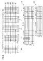
- FIG. 1 is a schematic view of an embodiment of the invention with respect to an SRAM (illustratively, 4kx32);
- FIG. 2 shows an example of a failure with respect to the SRAM of FIG. 1 ;
- FIG. 3 shows an example of a fill_array and of a shift_array, respectively
- FIGS. 4 to 13 show in a detailed view how, according to one embodiment of the method according to the invention, to fill the arrays of FIG. 3 during diagnosis of the failure shown in FIG. 2 ;
- FIG. 14 shows how a reference element is built from the fill_array at the end of a BIST run
- FIG. 15 shows how difference elements are built from the reference element and the fill_array
- FIG. 16 shows how the redundant IO is fixed using the difference elements shown in FIG. 15 ;
- FIG. 17 is a flow chart of a test repair sequence.
- FIG. 1 Such an SRAM 110 embodying an on chip diagnosis block according to the invention is shown in FIG. 1 .
- the SRAM 110 comprises an array 111 of storage elements accessible via wordlines (WLs) 112 and IO lines 114 .
- the word-register redundancy is carried out as external redundancy 120 (illustratively, having 3 redundant data registers 124 for addresses stored in corresponding redundant address registers 122 , and internal redundancy is the redundant IO only (IOR 116 ).
- the available redundancy of the embodiment shown in FIG. 1 consists of one complete redundant IO (IOR 116 ) inside the memory, and three external redundant register addresses 122 .
- the SRAM 110 includes an on-chip diagnosis block 119 configured to perform diagnosis operations described herein.
- FIG. 2 shows an example of a failure in the SRAM of FIG. 1 , which failure is repairable with the available redundancy. Detected failures are indicated in the figures as dots 118 in the array 111 .
- the on chip diagnosis block 119 comprises two mandatory arrays (“fill_array” 310 and “shift_array” 320 ), examples of which are shown in FIG. 3 .
- the fill_array 310 may include multiple lines 312 , each including a flag column 314 , address column 316 , and a column 318 for each IO line 114 .
- the shift_array 320 may include multiple lines 322 , each including a column 328 for each IO line 114 .
- FIGS. 4 to 13 show in a detailed view how to fill the two mandatory arrays (fill_array 310 and shift_array 320 ) for diagnosis according to one embodiment of an on chip diagnosis method according to the invention.
- a first defect on IO line 3 may be detected at a first address.
- a flag bit for the first line in the fill_array 310 may be set, and the first address may be stored in the address column.
- a bit may also be set in the column corresponding to IO line 3 , indicating the location of the detected defect.
- a bit may be set in the column corresponding to IO line 3 .
- a second set of 3 defects on IO lines 3 , 2 , and 0 may be detected at a second address.
- a flag bit for the second line in the fill_array 310 may be set, and the second address may be stored in the address column. Bits may also be set in the column corresponding to IO lines 3 , 2 , and 0 indicating the location of the detected defects.
- the first line may be shifted down to the second line and bits in the first line may be set in the columns corresponding to IO line 3 , 2 , and 0 .
- a third set of 4 defects on IO lines 3 , 2 , 1 , and 0 may be detected at a third address.
- a flag bit for the third line in the fill_array 310 may be set, and the third address may be stored in the address column.
- Bits may also be set in the column corresponding to IO lines 3 , 2 , 1 , and 0 indicating the location of the detected defects.
- the first and second lines may be shifted down, and bits in the first line may be set in the columns corresponding to IO line 3 , 2 , 1 , and 0 .
- a fourth defect on IO line 3 may be detected at a fourth address.
- a flag bit for the fourth line in the fill_array 310 may be set, and the fourth address may be stored in the address column.
- a bit may also be set in the column corresponding to IO line 3 , indicating the location of the detected defect.
- the first, second, and third lines may be shifted down, and a bit in the first line may be set in the column corresponding to IO line 3 , 2 , 1 , and 0 .
- a fifth defect on IO line 3 may be detected at a fifth address.
- the shift array is already filled up in the column corresponding to IO line 3 , no entry is made in the fill_array 310 .
- the shift_array 320 limits entries made to the fill_array 310 .
- sixth, seventh, and ninth defects are detected on IO line 3 , as illustrated in FIGS. 9 , 10 , and 12 , respectively, the two arrays are not changed.
- a flag bit for the fifth line in the fill_array 310 may be set, and the twelfth address may be stored in the address column.
- a bit may also be set in the column corresponding to IO line 0 , indicating the location of the detected defect.
- a bit in the next available column corresponding to IO line 0 may be set, line 3 in this example.
- a tenth defect on 10 line 1 may be detected at the second address.
- the second address is already stored in the fill_array 310 . Therefore, the bit corresponding to IO line 1 may be set to indicate this newly detected defect.
- the shift_array 320 a bit in the next available column corresponding to IO line 1 may be set, line 2 in this example.
- the defects are stored on chip during BIST and the diagnosis is carried out on chip, too, using said two arrays (fill_array 310 and shift_array 320 ).
- the reference element 1410 indicates for each line of the fill_array 310 , the number of faults for each address stored.
- the second element (called “difference element”) computes for each IO the difference between the reference element 1410 and a column of the fill_array 310 corresponding to each IO line.
- difference element computes for each IO the difference between the reference element 1410 and a column of the fill_array 310 corresponding to each IO line.
- FIG. 15 illustrates difference elements 1510 0 - 1510 3 generated for columns of the fill_array 310 corresponding to IO lines 0 - 3 , respectively.
- the memory of FIG. 1 with defects shown in FIG. 2 can now be repaired by replacing IO line 3 with the redundant IO (IOR 116 ), as shown in FIG. 16 .
- the difference element 1510 3 indicates which addresses have to be stored inside redundant address registers 122 (inside this element it is indicated by all bits set to “1”).
- FIG. 17 shows a flow chart of the exemplary operations 1700 of a test repair sequence in accordance with one embodiment of the present invention.
- a BIST is started and performed, at step 1704 . If the BIST test is done, as determined at step 1706 , the diagnostic operations described herein are performed, at step 1708 . If no faults are detected, as determined at step 1710 , the test sequence terminates, at step 1712 . If faults are detectable, unrepairable memory locations are flagged, at step 1716 . Redundancy is activated, at step 1718 , to fix repairable memory locations. The test sequence is terminated, at step 1720 .
Landscapes
- For Increasing The Reliability Of Semiconductor Memories (AREA)
- Tests Of Electronic Circuits (AREA)
- Techniques For Improving Reliability Of Storages (AREA)
Applications Claiming Priority (2)
| Application Number | Priority Date | Filing Date | Title |
|---|---|---|---|
| EPEP03292283.3 | 2003-09-16 | ||
| EP03292283A EP1517334B1 (de) | 2003-09-16 | 2003-09-16 | On-chip Diagnose-Vefahren und -Block zur Speicherreparatur mit gemischter Redundanz ("IO" Redundanz und "Word-register" Redundanz) |
Publications (2)
| Publication Number | Publication Date |
|---|---|
| US20050091563A1 US20050091563A1 (en) | 2005-04-28 |
| US7386769B2 true US7386769B2 (en) | 2008-06-10 |
Family
ID=34178640
Family Applications (1)
| Application Number | Title | Priority Date | Filing Date |
|---|---|---|---|
| US10/942,274 Expired - Fee Related US7386769B2 (en) | 2003-09-16 | 2004-09-16 | On chip diagnosis block with mixed redundancy |
Country Status (3)
| Country | Link |
|---|---|
| US (1) | US7386769B2 (de) |
| EP (1) | EP1517334B1 (de) |
| DE (1) | DE60334694D1 (de) |
Cited By (1)
| Publication number | Priority date | Publication date | Assignee | Title |
|---|---|---|---|---|
| US20070247937A1 (en) * | 2006-04-19 | 2007-10-25 | Elpida Memory, Inc. | Information processing system for calculating the number of redundant lines optimal for memory device |
Families Citing this family (4)
| Publication number | Priority date | Publication date | Assignee | Title |
|---|---|---|---|---|
| US7275190B2 (en) * | 2004-11-08 | 2007-09-25 | Micron Technology, Inc. | Memory block quality identification in a memory device |
| US7768847B2 (en) | 2008-04-09 | 2010-08-03 | Rambus Inc. | Programmable memory repair scheme |
| US10234507B2 (en) | 2016-07-20 | 2019-03-19 | International Business Machines Corporation | Implementing register array (RA) repair using LBIST |
| CN113435652B (zh) * | 2021-07-01 | 2023-01-24 | 贵州电网有限责任公司 | 一种一次设备缺陷诊断与预测方法 |
Citations (17)
| Publication number | Priority date | Publication date | Assignee | Title |
|---|---|---|---|---|
| US4460999A (en) * | 1981-07-15 | 1984-07-17 | Pacific Western Systems, Inc. | Memory tester having memory repair analysis under pattern generator control |
| US4751656A (en) * | 1986-03-10 | 1988-06-14 | International Business Machines Corporation | Method for choosing replacement lines in a two dimensionally redundant array |
| US5410687A (en) * | 1990-03-19 | 1995-04-25 | Advantest Corporation | Analyzing device for saving semiconductor memory failures |
| US5469390A (en) | 1993-09-16 | 1995-11-21 | Hitachi, Ltd. | Semiconductor memory system with the function of the replacement to the other chips |
| US5859804A (en) * | 1991-10-16 | 1999-01-12 | International Business Machines Corporation | Method and apparatus for real time two dimensional redundancy allocation |
| US5910921A (en) | 1997-04-22 | 1999-06-08 | Micron Technology, Inc. | Self-test of a memory device |
| US6032264A (en) * | 1997-04-22 | 2000-02-29 | Micron Technology, Inc. | Apparatus and method implementing repairs on a memory device |
| US6065134A (en) | 1996-02-07 | 2000-05-16 | Lsi Logic Corporation | Method for repairing an ASIC memory with redundancy row and input/output lines |
| US6141267A (en) | 1999-02-03 | 2000-10-31 | International Business Machines Corporation | Defect management engine for semiconductor memories and memory systems |
| US6172916B1 (en) * | 1999-02-12 | 2001-01-09 | Mitsubishi Denki Kabushiki Kaisha | Semiconductor memory device having a large band width and allowing efficient execution of redundant repair |
| US6304989B1 (en) | 1999-07-21 | 2001-10-16 | Credence Systems Corporation | Built-in spare row and column replacement analysis system for embedded memories |
| US20020108073A1 (en) * | 2001-02-02 | 2002-08-08 | Hughes Brian William | System for and method of operating a programmable column fail counter for redundancy allocation |
| US6502216B1 (en) | 1998-12-24 | 2002-12-31 | Advantest Corporation | Memory device testing apparatus |
| US6711705B1 (en) * | 1999-07-21 | 2004-03-23 | Advantest Corporation | Method of analyzing a relief of failure cell in a memory and memory testing apparatus having a failure relief analyzer using the method |
| US6928377B2 (en) * | 2003-09-09 | 2005-08-09 | International Business Machines Corporation | Self-test architecture to implement data column redundancy in a RAM |
| US7003704B2 (en) * | 2002-11-12 | 2006-02-21 | International Business Machines Corporation | Two-dimensional redundancy calculation |
| US7188274B2 (en) * | 2003-02-14 | 2007-03-06 | Logicvision, Inc. | Memory repair analysis method and circuit |
Family Cites Families (1)
| Publication number | Priority date | Publication date | Assignee | Title |
|---|---|---|---|---|
| EP1447813B9 (de) | 2003-02-12 | 2008-10-22 | Infineon Technologies AG | Verfahren und MBISR (Memory Built-In Self Repair) zum Reparieren eines Speichers |
-
2003
- 2003-09-16 DE DE60334694T patent/DE60334694D1/de not_active Expired - Lifetime
- 2003-09-16 EP EP03292283A patent/EP1517334B1/de not_active Expired - Fee Related
-
2004
- 2004-09-16 US US10/942,274 patent/US7386769B2/en not_active Expired - Fee Related
Patent Citations (17)
| Publication number | Priority date | Publication date | Assignee | Title |
|---|---|---|---|---|
| US4460999A (en) * | 1981-07-15 | 1984-07-17 | Pacific Western Systems, Inc. | Memory tester having memory repair analysis under pattern generator control |
| US4751656A (en) * | 1986-03-10 | 1988-06-14 | International Business Machines Corporation | Method for choosing replacement lines in a two dimensionally redundant array |
| US5410687A (en) * | 1990-03-19 | 1995-04-25 | Advantest Corporation | Analyzing device for saving semiconductor memory failures |
| US5859804A (en) * | 1991-10-16 | 1999-01-12 | International Business Machines Corporation | Method and apparatus for real time two dimensional redundancy allocation |
| US5469390A (en) | 1993-09-16 | 1995-11-21 | Hitachi, Ltd. | Semiconductor memory system with the function of the replacement to the other chips |
| US6065134A (en) | 1996-02-07 | 2000-05-16 | Lsi Logic Corporation | Method for repairing an ASIC memory with redundancy row and input/output lines |
| US5910921A (en) | 1997-04-22 | 1999-06-08 | Micron Technology, Inc. | Self-test of a memory device |
| US6032264A (en) * | 1997-04-22 | 2000-02-29 | Micron Technology, Inc. | Apparatus and method implementing repairs on a memory device |
| US6502216B1 (en) | 1998-12-24 | 2002-12-31 | Advantest Corporation | Memory device testing apparatus |
| US6141267A (en) | 1999-02-03 | 2000-10-31 | International Business Machines Corporation | Defect management engine for semiconductor memories and memory systems |
| US6172916B1 (en) * | 1999-02-12 | 2001-01-09 | Mitsubishi Denki Kabushiki Kaisha | Semiconductor memory device having a large band width and allowing efficient execution of redundant repair |
| US6304989B1 (en) | 1999-07-21 | 2001-10-16 | Credence Systems Corporation | Built-in spare row and column replacement analysis system for embedded memories |
| US6711705B1 (en) * | 1999-07-21 | 2004-03-23 | Advantest Corporation | Method of analyzing a relief of failure cell in a memory and memory testing apparatus having a failure relief analyzer using the method |
| US20020108073A1 (en) * | 2001-02-02 | 2002-08-08 | Hughes Brian William | System for and method of operating a programmable column fail counter for redundancy allocation |
| US7003704B2 (en) * | 2002-11-12 | 2006-02-21 | International Business Machines Corporation | Two-dimensional redundancy calculation |
| US7188274B2 (en) * | 2003-02-14 | 2007-03-06 | Logicvision, Inc. | Memory repair analysis method and circuit |
| US6928377B2 (en) * | 2003-09-09 | 2005-08-09 | International Business Machines Corporation | Self-test architecture to implement data column redundancy in a RAM |
Non-Patent Citations (2)
| Title |
|---|
| Akira Tanabe et al., "A 30-ns 64 Mb DRAM with Built-in Self-Test and Self-Repair Function", IEEE Journal of Solid-State Circuits, vol. 27, No. 11, pp. 1-7, Nov. 27, 1992, New York, US. |
| Best Solution Generator for Redundancy, IBM Technical Disclosure Bulletin, IBM Corp., vol. 29, No. 6, Nov. 1, 1986, pp. 2756-2758. |
Cited By (1)
| Publication number | Priority date | Publication date | Assignee | Title |
|---|---|---|---|---|
| US20070247937A1 (en) * | 2006-04-19 | 2007-10-25 | Elpida Memory, Inc. | Information processing system for calculating the number of redundant lines optimal for memory device |
Also Published As
| Publication number | Publication date |
|---|---|
| DE60334694D1 (de) | 2010-12-09 |
| EP1517334A1 (de) | 2005-03-23 |
| EP1517334B1 (de) | 2010-10-27 |
| US20050091563A1 (en) | 2005-04-28 |
Similar Documents
| Publication | Publication Date | Title |
|---|---|---|
| KR102117633B1 (ko) | 셀프 리페어 장치 | |
| US5377146A (en) | Hierarchical redundancy scheme for high density monolithic memories | |
| US7484138B2 (en) | Method and system for improving reliability of memory device | |
| US7085182B2 (en) | Fuse blowing interface for a memory chip | |
| US20050041491A1 (en) | Repair apparatus and method for semiconductor memory device to be selectively programmed for wafer-level test or post package test | |
| US5831913A (en) | Method of making a memory fault-tolerant using a variable size redundancy replacement configuration | |
| JPH05166396A (ja) | 半導体メモリ装置 | |
| US20060242492A1 (en) | Method and apparatus for masking known fails during memory tests readouts | |
| US6937531B2 (en) | Memory device and method of storing fail addresses of a memory cell | |
| US6490210B2 (en) | Semiconductor memory integrated circuit employing a redundant circuit system for compensating for defectiveness | |
| Kim et al. | A BISR (built-in self-repair) circuit for embedded memory with multiple redundancies | |
| US7359260B2 (en) | Repair of memory cells | |
| US11651831B2 (en) | Redundancy analysis circuit and memory system including the same | |
| US9847142B2 (en) | Semiconductor apparatus and repair method thereof | |
| US8468401B2 (en) | Apparatus and method for manufacturing a multiple-chip memory device with multi-stage testing | |
| US20040153725A1 (en) | ROM redundancy in ROM embedded DRAM | |
| US7016242B2 (en) | Semiconductor memory apparatus and self-repair method | |
| JP3967704B2 (ja) | 半導体記憶装置とそのテスト方法 | |
| US7386769B2 (en) | On chip diagnosis block with mixed redundancy | |
| US20030204798A1 (en) | Optimized ECC/redundancy fault recovery | |
| US6870782B2 (en) | Row redundancy memory repair scheme with shift to eliminate timing penalty | |
| JPS62250599A (ja) | 半導体メモリ装置 | |
| EP1408512B1 (de) | Verfahren zum Speichern von Fehlern einer Speichervorrichtung in einem Diagnosefeld mit minimaler Speicherkapazität | |
| US6754113B2 (en) | Topography correction for testing of redundant array elements | |
| Adams | BIST and Redundancy: Memory Self Test |
Legal Events
| Date | Code | Title | Description |
|---|---|---|---|
| AS | Assignment |
Owner name: INFINEON TECHNOLOGIES AG, GERMANY Free format text: ASSIGNMENT OF ASSIGNORS INTEREST;ASSIGNORS:JALLAMION-GRIVE, YANNIS;COLLURA, MICHEL;VIAL, JEAN-CHRISTOPHE;REEL/FRAME:015498/0384;SIGNING DATES FROM 20041126 TO 20041203 |
|
| FEPP | Fee payment procedure |
Free format text: PAYOR NUMBER ASSIGNED (ORIGINAL EVENT CODE: ASPN); ENTITY STATUS OF PATENT OWNER: LARGE ENTITY Free format text: PAYER NUMBER DE-ASSIGNED (ORIGINAL EVENT CODE: RMPN); ENTITY STATUS OF PATENT OWNER: LARGE ENTITY |
|
| STCF | Information on status: patent grant |
Free format text: PATENTED CASE |
|
| CC | Certificate of correction | ||
| FPAY | Fee payment |
Year of fee payment: 4 |
|
| FPAY | Fee payment |
Year of fee payment: 8 |
|
| FEPP | Fee payment procedure |
Free format text: MAINTENANCE FEE REMINDER MAILED (ORIGINAL EVENT CODE: REM.); ENTITY STATUS OF PATENT OWNER: LARGE ENTITY |
|
| LAPS | Lapse for failure to pay maintenance fees |
Free format text: PATENT EXPIRED FOR FAILURE TO PAY MAINTENANCE FEES (ORIGINAL EVENT CODE: EXP.); ENTITY STATUS OF PATENT OWNER: LARGE ENTITY |
|
| STCH | Information on status: patent discontinuation |
Free format text: PATENT EXPIRED DUE TO NONPAYMENT OF MAINTENANCE FEES UNDER 37 CFR 1.362 |
|
| FP | Lapsed due to failure to pay maintenance fee |
Effective date: 20200610 |