US7325218B2 - Wiring method, program, and apparatus - Google Patents
Wiring method, program, and apparatus Download PDFInfo
- Publication number
- US7325218B2 US7325218B2 US11/062,617 US6261705A US7325218B2 US 7325218 B2 US7325218 B2 US 7325218B2 US 6261705 A US6261705 A US 6261705A US 7325218 B2 US7325218 B2 US 7325218B2
- Authority
- US
- United States
- Prior art keywords
- wiring
- nets
- adjacent spacing
- condition
- spacing condition
- Prior art date
- Legal status (The legal status is an assumption and is not a legal conclusion. Google has not performed a legal analysis and makes no representation as to the accuracy of the status listed.)
- Expired - Fee Related, expires
Links
Images


Classifications
-
- G—PHYSICS
- G06—COMPUTING OR CALCULATING; COUNTING
- G06F—ELECTRIC DIGITAL DATA PROCESSING
- G06F30/00—Computer-aided design [CAD]
- G06F30/30—Circuit design
- G06F30/36—Circuit design at the analogue level
- G06F30/367—Design verification, e.g. using simulation, simulation program with integrated circuit emphasis [SPICE], direct methods or relaxation methods
-
- G—PHYSICS
- G06—COMPUTING OR CALCULATING; COUNTING
- G06F—ELECTRIC DIGITAL DATA PROCESSING
- G06F30/00—Computer-aided design [CAD]
- G06F30/30—Circuit design
- G06F30/39—Circuit design at the physical level
- G06F30/394—Routing
Definitions
- the invention relates to wiring method, program, and apparatus in a layout design of an LSI and, more particularly, to wiring method, program, and apparatus which take crosstalks and a wiring delay into consideration.
- an influence of a wiring delay is larger than that of a gate delay due to micro miniaturization of a transistor size.
- An adjacent load capacity can be mentioned as one of causes of the wiring delay.
- An influence of noises caused by crosstalks is also large and the adjacent load capacity can be also mentioned as one of causes of the noises. Therefore, a wiring technique to reduce the adjacent load capacity at the time of automatic wiring is demanded.
- the conventional automatic wiring when a certain net is automatically wired on the basis of a net list, a minimum adjacent spacing condition which does not become a wiring violation is given and the wiring is performed. Even if a load condition to reduce the adjacent load capacity is given, it is given to all nets and the nets are automatically wired.
- JP-A-5-181936 JP-A-6-124321, JP-A-5-160375, JP-A-5-243383, JP-A-9-147009, JP-A-10-189746, and JP-A-2003-303217.
- the adjacent load capacity is added with respect to an important path and the problems of the increase in wiring delay and the increase in crosstalk noises are caused. Even if the automatic wiring is executed by using the load condition for the adjacent capacity, since it is executed for all of the nets as targets, such a problem that the apparatus enters the state where it is difficult to complete the wiring due to a lack of channels in terms of a relation with an integration degree.
- wiring method, program, and apparatus which can efficiently solve the problem by giving a proper adjacent spacing con dition only to nets having such a problem that a wiring delay or crosstalks are caused are provided.
- the invention provides a wiring method of designing a semiconductor circuit such as an LSI or the like.
- the wiring method of the invention comprises:
- the wiring condition changing step a parameter file in which the second adjacent spacing condition for eliminating the noise errors of the error nets has been set every net name is formed, and in the re-wiring processing step, the second adjacent spacing condition in the parameter file is given to the error nets and the wiring process is executed again.
- a parameter file in which the second adjacent spacing condition for eliminating the noise errors of the error nets has been set in accordance with a net type is formed, and similarly, in the re-wiring processing step, the second adjacent spacing condition in the parameter file is given to the error nets and the wiring process is executed again.
- a parameter file in which the second adjacent spacing condition for eliminating the noise errors of the error nets has been set in accordance with a wiring layer is formed, and similarly, in the re-wiring processing step, the second adjacent spacing condition in the parameter file is given to the error nets and the wiring process is executed again.
- a parameter file in which a distance between the nets or the number of grids between the nets has been set as a second adjacent spacing condition of the error nets is formed.
- a minimum adjacent spacing condition is given as a first adjacent spacing condition and the wiring process is executed.
- the invention provides a wiring program which is executed by a computer.
- the wiring program of the invention allows the computer to execute:
- a wiring processing step wherein a first adjacent spacing condition which does not become a wiring violation is given and a wiring process is executed on the basis of a net list of a semiconductor circuit;
- noise analyzing step wherein error nets in which noise errors have occurred are extracted by analyzing noises of a wiring formed in the wiring processing step
- a wiring condition changing step wherein a second adjacent spacing condition for eliminating the noise errors of the error nets extracted in the noise analyzing step is set;
- a re-wiring processing step wherein the second adjacent spacing condition is given to the error nets, the first adjacent spacing condition is given to nets other than the error nets, and the wiring process is executed again on the basis of the net list.
- the invention provides a wiring apparatus for designing a semiconductor circuit such as an LSI or the like.
- the wiring apparatus of the invention comprises:
- a wiring processing unit which executes a wiring process by giving a first adjacent spacing condition that does not become a wiring violation on the basis of a net list of the semiconductor circuit
- noise analyzing unit which extracts error nets in which noise errors have occurred by analyzing noises of a wiring formed by the wiring processing unit
- a wiring condition changing unit which gives a second adjacent spacing condition for eliminating the noise errors to the error nets and allows the wiring processing unit to execute the wiring process again on the basis of the net list in the state where the first adjacent spacing condition has been given to nets other than the error nets.
- the noises are analyzed, and the nets which do not satisfy a noise restriction that takes the crosstalks or the wiring delay into consideration are extracted as error nets in which the noise errors have occurred.
- a new adjacent spacing condition for widening a wiring interval is set as a parameter for eliminating the noise error, the wiring process is executed again, and the noise error can be eliminated.
- a designing process which takes the adjacent load capacity (coupling capacity) into consideration has been executed.
- the wiring process in which the adjacent spacing condition has been changed is executed again to the error nets, as a target, in which the noise error still occurs by the noise analysis as a result of the wiring process, so that the wiring process can be efficiently and successfully completed in a short time.
- the number of error nets obtained by the noise analysis after the wiring process is less than, for example, 100 .
- the invention by giving the adjacent spacing condition for eliminating the noise errors to the error nets and executing the wiring process again, the errors of the target nets are successively eliminated and the automatic wiring can be efficiently and successfully completed in a short time.
- the parameter of the adjacent spacing condition which is given to the error nets is formed in correspondence to the net name, the net type, or the wiring layer.
- the parameter of the adjacent spacing condition in the case where the error nets occurred with respect to it is preferentially set, thereby rescuing.
- the parameter of the adjacent spacing condition corresponding to the wiring layer since the first and second layers are cell layers and a possibility of existence of a long wiring which causes the crosstalks is low, an external parameter of the adjacent condition is set every layer with respect to the layers where the longer nets are wired and the nets in which the noise errors have occurred can be eliminated.
- FIG. 1 is a block diagram of a whole construction of an LSI designing system
- FIG. 2 is a block diagram of a functional construction of a wiring apparatus according to the invention.
- FIG. 3 is an explanatory diagram of a hardware environment of a computer to which the wiring apparatus of FIG. 2 is applied;
- FIGS. 4A to 4C are explanatory diagrams of parameter files in FIG. 2 ;
- FIGS. 5A and 5B are explanatory diagrams of a wiring process for eliminating error nets according to the invention.
- FIG. 6 is a flowchart for the wiring process according to the invention.
- FIG. 1 is a block diagram of a whole construction of an LSI designing system to which a wiring method of the invention is applied.
- the LSI designing system comprises: a system specification designing unit 10 ; a function designing unit 12 ; a logic designing unit 14 ; a circuit designing unit 16 ; a layout designing unit 18 ; a design verifying unit 20 ; and an LSI manufacturing unit 22 .
- a layout processing unit 24 and a wiring processing unit 26 are provided for the layout designing unit 18 .
- the wiring method of the invention is applied to the wiring processing unit 26 .
- the system specification designing unit 10 determines into which functional blocks the whole system is divided and how it operates in order to realize a target system specification of an LSI. An operation simulator or a system simulator is used to examine validity of a design result.
- the function designing unit 12 makes a design at a register transfer level (RT level) for deciding an internal structure and the operation of a functional block.
- a function simulator is used to verify the design result.
- the logic designing unit 14 designs a logic circuit at a gate level.
- a logic simulator, a timing simulator, or the like is used to confirm the operation.
- the circuit designing unit 16 designs a transistor circuit.
- a circuit simulator is used to examine characteristics of the designed circuit.
- the layout designing unit 18 executes a process for converting a circuit diagram into a layout wiring of a device having a physical shape and dimensions and a layout, a wiring program, and the like corresponding to an automatic design are used.
- the layout processing unit 24 in the layout designing unit 18 decides a shape of a device such as transistor, cell, or the like having actual physical dimensions and its layout position from logical information such as logic circuit or transistor circuit.
- the wiring processing unit 26 provided for the layout designing unit 18 decides a design among the cells arranged by the layout processing unit 24 so as to satisfy a design and various restricting conditions.
- a method of dividing the line connection into two stages of global wiring and detailed wiring is ordinarily used as a wiring method. According to the global wiring, each net is divided into specific wiring areas and the wirings are allocated, and which wiring area is used while avoiding a direct jam is determined.
- the design verifying unit 20 executes the following processes: a design rule check (DRC) to examine rule violation of the design dimensions with respect to the designed layout; a forming check to examine a line extracting and forming algorithm for forming line forming information from the layout; an electric rule check to examine dimension requesting characteristics of the transistor and the presence or absence of a short-circuit of a power wiring; and the like.
- DRC design rule check
- a forming check to examine a line extracting and forming algorithm for forming line forming information from the layout
- an electric rule check to examine dimension requesting characteristics of the transistor and the presence or absence of a short-circuit of a power wiring; and the like.
- the invention is applied to the wiring processing unit 26 in the layout designing unit 18 .
- the wiring process is executed on the basis of a net list, first, the minimum adjacent spacing condition is given as a first adjacent spacing condition and the wiring process is executed. With respect to a result of the wiring process, noises are analyzed. Error nets in which noise errors have occurred are extracted by the noise analysis. A second adjacent spacing condition for eliminating the noise errors is set to the error nets, the wiring process is executed again, and the noise analysis and the re-wiring process due to the change in the adjacent spacing condition to the error nets are repeated until the noise errors are eliminated.
- FIG. 2 is a block diagram of a functional construction of a wiring apparatus according to the invention.
- a net list 32 is provided for a wiring apparatus 30 of the invention. Net list data obtained after the design was finished in the circuit designing unit 16 as shown in FIG. 1 has been stored in the net list 32 .
- a parameter file 34 is provided for the wiring apparatus 30 .
- a parameter to widen an interval between the error nets as an adjacent spacing condition which is used in a re-wiring process of the error nets extracted by the noise analysis of the result of the wiring process of the invention, that is, as a second spacing condition is formed and stored in the parameter file 34 .
- the wiring apparatus 30 comprises: a wiring processing unit 36 ; a layout data file 38 ; a noise analyzing unit 40 ; a wiring condition changing unit 42 ; and an output processing unit 44 .
- Layout design data obtained after completion of the process in the wiring apparatus 30 is outputted as mask pattern data 46 after completion of the design verification.
- the wiring processing unit 36 provided for the wiring apparatus 30 gives the minimum adjacent spacing condition (first adjacent spacing condition) which does not become the wiring violation on the basis of the net list 32 and executes the wiring process.
- the wiring result by the wiring processing unit 36 is temporarily stored in the layout data file 38 .
- the noise analyzing unit 40 executes the noise analysis of the wiring result in the layout data file 38 as a target.
- the error nets in which the noise errors have occurred are extracted by the noise analysis.
- the crosstalks occur, a change is caused in a signal delay or they become a cause of an illegal transition of the logic and an object of performance of a chip cannot be accomplished. Therefore, the net in this case is determined to be the error net and extracted.
- the wiring condition changing unit 42 forms an adjacent spacing condition (second adjacent spacing condition) for eliminating the noise errors of the error nets extracted by the noise analyzing unit 40 , stores it into the parameter file 34 , and thereafter, gives the adjacent spacing condition in the parameter file 34 to the error nets. With respect to the nets other than the error nets, the wiring condition changing unit 42 gives the minimum adjacent spacing condition which was used first and allows the wiring processing unit 36 to execute the wiring process again under such a condition. The result of the wiring process executed under the adjacent spacing condition formed with respect to the error nets by the wiring condition changing unit 42 is stored into the layout data file 38 . After that, it is analyzed by the noise analyzing unit 40 again. If the noise restriction is satisfied, it is determined that the wiring process is successful, thereby instructing the output processing unit 44 to output the wiring result.
- second adjacent spacing condition for eliminating the noise errors of the error nets extracted by the noise analyzing unit 40 , stores it into the parameter file 34 , and thereafter, gives the adjacent spacing condition in the parameter file 34 to the error nets. With respect
- the adjacent spacing condition (second adjacent spacing condition) necessary to eliminate the noise errors of the residual error nets is further formed in the wiring condition changing unit 42 .
- This parameter is stored into the parameter file 34 .
- the adjacent spacing condition in the parameter file 34 is given to the residual error nets.
- the wiring process of the wiring processing unit 36 is again repeated in the state where the first adjacent spacing condition has been given.
- the parameter is changed so as to widen the wiring interval each time the wiring process is executed.
- the maximum value of the wiring interval is set and when the wiring interval reaches the maximum value due to the change in the adjacent spacing condition, the adjacent spacing condition cannot be changed any more. Therefore, it is regarded that the wiring process failed, the designing process is returned to the upstream side, and the designing process is repeated again.
- the designing process which takes the adjacent load capacity (coupling capacity) into consideration is executed in the designing process of the upstream side such as function designing unit 12 , logic designing unit 14 , or circuit designing unit 16 shown in FIG. 1 .
- the error nets are extracted by the error analysis in the alternation of the wiring process, the adjacent spacing condition for the error nets is lightened, thereby allowing the wiring process to be successfully completed.
- the wiring apparatus 30 in FIG. 2 is realized by, for example, hardware resources of a computer as shown in FIG. 3 .
- a RAM 102 a hard disk controller (software) 104 , a floppy disk driver (software) 110 , a CD-ROM driver (software) 114 , a mouse controller 118 , a keyboard controller 122 , a display controller 126 , and a communicating board 130 are connected to a bus 101 of a CPU 100 .
- a hard disk drive 106 is connected to the hard disk controller 104 . Programs to execute the wiring process of the invention have been loaded in the hard disk controller 104 . When the computer is activated, the necessary program is called from the hard disk drive 106 , developed into the RAM 102 , and executed by the CPU 100 .
- a floppy disk drive (hardware) 112 is connected to the floppy disk driver 110 and data can be written and read out into/from a floppy disk (registered trademark).
- a CD drive (hardware) 116 is connected to the CD-ROM driver 114 and data or programs stored in a CD can be read out.
- the mouse controller 118 transfers the inputting operation of a mouse 120 to the CPU 100 .
- the keyboard controller 122 transfers the inputting operation of a keyboard 124 to the CPU 100 .
- the display controller 126 allows a display unit 128 to display data.
- the communicating board 130 communicates with an external apparatus via a network by using a communicating line 132 including a wireless manner.
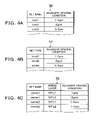
- FIGS. 4A to 4C are explanatory diagrams of parameter information which is stored into the parameter file 34 .
- FIG. 4A shows a net name parameter file 48 .
- the adjacent spacing condition for eliminating the noise errors is formed and registered with respect to net names net 1 , net 2 , net 3 , . . . of the error nets extracted by the noise analysis.
- the adjacent spacing condition is a condition in which the minimum adjacent spacing condition (first adjacent spacing condition) which is used as a default has been lightened.
- a distance ( ⁇ m) between the nets or the number of grids (grid) between the nets is used as a specific parameter of the adjacent spacing condition.
- the error nets due to the crosstalks are discriminated. With respect to the crosstalks, the nets locating on both sides of the net in which a signal which becomes a cause of the noises flows become the error nets in which the noise errors occur.
- the parameter as an adjacent spacing condition for eliminating the noise errors is formed and registered every net name of the error nets in which the noise errors due to the crosstalks have occurred. This parameter is used at the time of executing the wiring process again.
- FIG. 4B is an explanatory diagram of a net type parameter file 50 .
- the parameter of the adjacent spacing condition for eliminating the noise errors of the error nets is registered as a distance ( ⁇ m) between the nets or the number of grids (grid) between the nets in correspondence to the net type.
- a net type registered in the net type parameter file 50 for example, it can be classified into a clock net and the other nets.
- the clock net is the most critical net
- the parameter setting for eliminating the noise errors in the case where the clock net is determined to be the error net is preferentially made.
- the adjacent spacing condition is set at a low priority.
- the clock net is the error net
- the sufficient value of the distance between the nets or the number of grids between the nets is formed and set as a parameter and a large value is used as an adjacent spacing parameter condition for the clock net.
- the parameter of a small value is used as an adjacent spacing condition, even if the value of the parameter for eliminating the noises of the clock net is increased, the apparatus is prevented from entering the state where it is difficult to complete the wiring due to the lack of channels in view of the relation with the correction activation of the whole chip in the re-writing process.
- FIG. 4C is an explanatory diagram of a wiring layer parameter file 52 .
- the wiring layer parameter file 52 is constructed by the net name, the wiring layer, and the adjacent spacing condition.
- the wiring layer parameter file 52 as shown in FIG. 4C is provided and the parameter as an adjacent spacing condition for eliminating the net errors is formed and registered in dependence on the net name and the wiring layer.
- the distance between the nets or the number of grids between the nets as an adjacent spacing condition (second adjacent spacing condition) for eliminating the noise errors of the error nets has been registered.
- an increase amount of the distance between the nets or the number of grids between the nets of the minimum adjacent spacing condition used in the first wiring process can be also registered.
- FIGS. 5A and 5B are explanatory diagrams of the wiring process for eliminating the error nets according to the invention.
- FIG. 5A shows a wiring result obtained by executing the wiring process by giving a distance W 1 between the nets according to the minimum adjacent spacing condition as a default.
- a net 62 is arranged between cells 56 - 1 and 56 - 2 arranged in a chip 54
- a net 64 is wired between cells 58 - 1 and 58 - 2
- a net 66 is wired between cells 60 - 1 and 60 - 2 .
- the diagram shows a perspective view of a construction in which crossing portions of the nets 62 , 64 , and 66 are arranged in the different wiring layers and the wiring layers are connected by through holes.
- the net in which the noise error due to the crosstalks actually occurs is the net that is adjacent to the net which becomes a cause of the noises.
- the adjacent nets 62 and 66 becomes the error nets in which the noise error due to the crosstalks is caused.
- a relation between the signal sources in the nets 62 , 64 , and 66 and the error nets in which the noise error due to the crosstalks is caused is a relative relation.
- a parameter in which the adjacent spacing condition necessary to eliminate the noise errors that is, the distance between the nets is set to W 2 widened from the default W 1 is formed and registered into the parameter file 34 shown in FIG. 2 .
- the adjacent spacing condition which gives the distance W 2 between the nets registered in the parameter file 34 is given to the nets 62 , 64 , and 66 which were determined to be the error nets and the wiring process is executed again, so that the wiring result of FIG. 5B can be obtained.
- the noise analysis is performed with respect to the wiring result of FIG. 5B .
- the wiring process can be completed.
- an adjacent spacing condition is formed by using a larger distance W 3 between the nets as a parameter and registered. It is given to the error nets again, the wiring process is executed, and the process is repeated until the distance between the nets reaches the allowable maximum value as an adjacent spacing condition.
- FIG. 6 is a flowchart for the wiring process according to the invention.
- the wiring process is executed on the basis of the net list 32 in step S 1 .
- the wiring process is executed by giving the minimum adjacent spacing condition.
- the noise analysis is performed with respect to the wiring result of step S 1 .
- step S 3 whether or not the nets which do not satisfy the noise restriction exist is discriminated. If the nets which do not satisfy the noise restriction exist, step S 4 follows.
- the nets in which the noise errors have occurred are extracted.
- the adjacent spacing condition (second adjacent spacing condition) for eliminating the noise errors is formed and the parameter file 34 in which such a condition has been registered is formed.
- the adjacent spacing condition in the parameter file is given to the error nets. With respect to the nets other than the error nets, the same minimum adjacent spacing condition as that in step S 1 is given to them and the wiring process is executed again.
- step S 6 If the wiring process does not fail due to the lack of channels or the like but is successful in step S 6 , the processing routine is returned to step S 2 and the noise analysis is performed. If the net which does not satisfy the noise restriction does not exist in step S 3 , this means that the wiring is successful, so that a series of processes is finished. If the wiring is unsuccessful due to the lack of channels in step S 6 , an error is notified in step S 7 and the processing routine is finished. In this case, the processing routine is returned to the design stage on the upstream side and it is newly designed. In steps S 2 to S 6 in FIG. 6 , the adjacent spacing condition is changed and the wiring process is repeated until the error nets which do not satisfy the noise restriction do not exist. However, actually, when the adjacent spacing condition reaches the maximum value, the processing routine is finished as an error.
- the invention provides a wiring program which is used in the wiring process in the LSI designing system, and this wiring program is realized as a program having a processing procedure according to contents of the flowchart of FIG. 6 .
Landscapes
- Engineering & Computer Science (AREA)
- Computer Hardware Design (AREA)
- Physics & Mathematics (AREA)
- Theoretical Computer Science (AREA)
- Evolutionary Computation (AREA)
- Geometry (AREA)
- General Engineering & Computer Science (AREA)
- General Physics & Mathematics (AREA)
- Computer Networks & Wireless Communication (AREA)
- Microelectronics & Electronic Packaging (AREA)
- Design And Manufacture Of Integrated Circuits (AREA)
Abstract
Description
- a wiring processing step wherein a first adjacent spacing condition which does not become a wiring violation is given and a wiring process is executed on the basis of a net list of the semiconductor circuit;
- a noise analyzing step wherein error nets in which noise errors have occurred are extracted by analyzing noises of a wiring formed in the wiring processing step;
- a wiring condition changing step wherein a second adjacent spacing condition for eliminating the noise errors of the error nets extracted in the noise analyzing step is set; and
- a re-wiring processing step wherein the second adjacent spacing condition is given to the error nets, the first adjacent spacing condition is given to nets other than the error nets, and the wiring process is executed again on the basis of the net list.
(line width×length)=(costs)
with respect to the net in which the crosstalks are caused. If the calculated costs of this net exceeds predetermined crosstalk costs which have been determined as a noise restricting condition, this net is determined to be the error net. That is, in the design of the LSI, the error including the crosstalks is caused by the capacity which is coupled between the adjacent wirings, that is, the adjacent load capacity (coupling capacity). When the crosstalks occur, a change is caused in a signal delay or they become a cause of an illegal transition of the logic and an object of performance of a chip cannot be accomplished. Therefore, the net in this case is determined to be the error net and extracted.
Claims (9)
Applications Claiming Priority (2)
| Application Number | Priority Date | Filing Date | Title |
|---|---|---|---|
| JP2004343339A JP2006155120A (en) | 2004-11-29 | 2004-11-29 | Wiring method, program and apparatus |
| JPJP2004-343339 | 2004-11-29 |
Publications (2)
| Publication Number | Publication Date |
|---|---|
| US20060117289A1 US20060117289A1 (en) | 2006-06-01 |
| US7325218B2 true US7325218B2 (en) | 2008-01-29 |
Family
ID=36568589
Family Applications (1)
| Application Number | Title | Priority Date | Filing Date |
|---|---|---|---|
| US11/062,617 Expired - Fee Related US7325218B2 (en) | 2004-11-29 | 2005-02-22 | Wiring method, program, and apparatus |
Country Status (2)
| Country | Link |
|---|---|
| US (1) | US7325218B2 (en) |
| JP (1) | JP2006155120A (en) |
Cited By (3)
| Publication number | Priority date | Publication date | Assignee | Title |
|---|---|---|---|---|
| US20100030358A1 (en) * | 2007-05-28 | 2010-02-04 | Fujitsu Limited | Automatic wiring apparatus, automatic wiring method, automatic wiring program and computer-readable recording medium on which the program is recorded |
| US10896283B1 (en) * | 2019-08-16 | 2021-01-19 | International Business Machines Corporation | Noise-based optimization for integrated circuit design |
| US20220004693A1 (en) * | 2020-07-06 | 2022-01-06 | Synopsys, Inc. | Incremental routing based pin assignment |
Families Citing this family (11)
| Publication number | Priority date | Publication date | Assignee | Title |
|---|---|---|---|---|
| JP4501728B2 (en) * | 2005-03-08 | 2010-07-14 | 日本電気株式会社 | Crosstalk error control device, crosstalk error control method, and crosstalk error control program |
| US8161425B1 (en) * | 2006-04-19 | 2012-04-17 | Cadence Design Systems, Inc. | Method and system for implementing timing aware metal fill |
| JP2008021001A (en) * | 2006-07-11 | 2008-01-31 | Matsushita Electric Ind Co Ltd | Pattern correction device, pattern optimization device, and integrated circuit design device |
| JP4856512B2 (en) * | 2006-10-17 | 2012-01-18 | シャープ株式会社 | Manufacturing method and manufacturing program for semiconductor integrated circuit |
| US20080148213A1 (en) * | 2006-11-15 | 2008-06-19 | Moussadek Belaidi | Routing method for reducing coupling between wires of an electronic circuit |
| US8032851B2 (en) * | 2006-11-15 | 2011-10-04 | International Business Machines Corporation | Structure for an integrated circuit design for reducing coupling between wires of an electronic circuit |
| JP2008210858A (en) * | 2007-02-23 | 2008-09-11 | Fujitsu Ltd | Semiconductor integrated circuit design method, design apparatus, and CAD program |
| WO2009084092A1 (en) * | 2007-12-27 | 2009-07-09 | Fujitsu Limited | Macro layout verifying device and method |
| WO2011096058A1 (en) * | 2010-02-03 | 2011-08-11 | 富士通株式会社 | Circuit design method, circuit design system and program |
| JP5482774B2 (en) | 2011-12-16 | 2014-05-07 | 株式会社デンソー | Board wiring design method |
| WO2013140471A1 (en) * | 2012-03-23 | 2013-09-26 | 日本電気株式会社 | Design rule checking system, method, and non-transitory computer readable medium having program stored therein |
Citations (14)
| Publication number | Priority date | Publication date | Assignee | Title |
|---|---|---|---|---|
| JPH05160375A (en) | 1991-12-10 | 1993-06-25 | Fujitsu Ltd | Automatic routing method |
| JPH05181936A (en) | 1991-12-27 | 1993-07-23 | Fujitsu Ltd | Wiring method |
| JPH05243383A (en) | 1992-03-02 | 1993-09-21 | Hitachi Ltd | Automatic wiring method |
| JPH06124321A (en) | 1992-10-09 | 1994-05-06 | Nec Corp | Automatic wiring processing method |
| JPH09147009A (en) | 1995-11-24 | 1997-06-06 | Hitachi Ltd | Crosstalk delay determination method and parallel wiring length limitation method |
| JPH10189746A (en) | 1996-12-27 | 1998-07-21 | Oki Electric Ind Co Ltd | Wiring layout method for lsi logic circuit |
| US6058256A (en) * | 1996-09-26 | 2000-05-02 | Lucent Technologies Inc. | Technique for effectively routing conduction paths in circuit layouts |
| JP2003303217A (en) | 2002-04-08 | 2003-10-24 | Matsushita Electric Ind Co Ltd | How to avoid crosstalk |
| US20040015806A1 (en) * | 2002-07-19 | 2004-01-22 | Frank Mark D. | Inter-signal proximity verification in an integrated circuit |
| US20040103386A1 (en) * | 2002-11-26 | 2004-05-27 | Becer Murat R. | Noise analysis for an integrated circuit model |
| US20050132309A1 (en) * | 2003-12-16 | 2005-06-16 | Prashant Saxena | Automated noise convergence for cell-based integrated circuit design |
| US6968521B2 (en) * | 2002-03-20 | 2005-11-22 | Fujitsu Limited | Method, apparatus and program product for automatic placement and routing of integrated circuit |
| US20060026539A1 (en) * | 2004-07-28 | 2006-02-02 | Alexander Tetelbaum | Method of automated repair of crosstalk violations and timing violations in an integrated circuit design |
| US20070079274A1 (en) * | 2005-10-05 | 2007-04-05 | Lsi Logic Corporation | Method and computer program for detailed routing of an integrated circuit design with multiple routing rules and net constraints |
-
2004
- 2004-11-29 JP JP2004343339A patent/JP2006155120A/en active Pending
-
2005
- 2005-02-22 US US11/062,617 patent/US7325218B2/en not_active Expired - Fee Related
Patent Citations (15)
| Publication number | Priority date | Publication date | Assignee | Title |
|---|---|---|---|---|
| JPH05160375A (en) | 1991-12-10 | 1993-06-25 | Fujitsu Ltd | Automatic routing method |
| JPH05181936A (en) | 1991-12-27 | 1993-07-23 | Fujitsu Ltd | Wiring method |
| JPH05243383A (en) | 1992-03-02 | 1993-09-21 | Hitachi Ltd | Automatic wiring method |
| JPH06124321A (en) | 1992-10-09 | 1994-05-06 | Nec Corp | Automatic wiring processing method |
| JPH09147009A (en) | 1995-11-24 | 1997-06-06 | Hitachi Ltd | Crosstalk delay determination method and parallel wiring length limitation method |
| US6058256A (en) * | 1996-09-26 | 2000-05-02 | Lucent Technologies Inc. | Technique for effectively routing conduction paths in circuit layouts |
| JPH10189746A (en) | 1996-12-27 | 1998-07-21 | Oki Electric Ind Co Ltd | Wiring layout method for lsi logic circuit |
| US6080206A (en) | 1996-12-27 | 2000-06-27 | Oki Electric Industry Co., Ltd. | Method of laying out interconnections |
| US6968521B2 (en) * | 2002-03-20 | 2005-11-22 | Fujitsu Limited | Method, apparatus and program product for automatic placement and routing of integrated circuit |
| JP2003303217A (en) | 2002-04-08 | 2003-10-24 | Matsushita Electric Ind Co Ltd | How to avoid crosstalk |
| US20040015806A1 (en) * | 2002-07-19 | 2004-01-22 | Frank Mark D. | Inter-signal proximity verification in an integrated circuit |
| US20040103386A1 (en) * | 2002-11-26 | 2004-05-27 | Becer Murat R. | Noise analysis for an integrated circuit model |
| US20050132309A1 (en) * | 2003-12-16 | 2005-06-16 | Prashant Saxena | Automated noise convergence for cell-based integrated circuit design |
| US20060026539A1 (en) * | 2004-07-28 | 2006-02-02 | Alexander Tetelbaum | Method of automated repair of crosstalk violations and timing violations in an integrated circuit design |
| US20070079274A1 (en) * | 2005-10-05 | 2007-04-05 | Lsi Logic Corporation | Method and computer program for detailed routing of an integrated circuit design with multiple routing rules and net constraints |
Cited By (5)
| Publication number | Priority date | Publication date | Assignee | Title |
|---|---|---|---|---|
| US20100030358A1 (en) * | 2007-05-28 | 2010-02-04 | Fujitsu Limited | Automatic wiring apparatus, automatic wiring method, automatic wiring program and computer-readable recording medium on which the program is recorded |
| US8219955B2 (en) * | 2007-05-28 | 2012-07-10 | Fujitsu Limited | Automatically wiring circuit by setting and changing reference to design quality relating to electric characteristic |
| US10896283B1 (en) * | 2019-08-16 | 2021-01-19 | International Business Machines Corporation | Noise-based optimization for integrated circuit design |
| US20220004693A1 (en) * | 2020-07-06 | 2022-01-06 | Synopsys, Inc. | Incremental routing based pin assignment |
| US11853680B2 (en) * | 2020-07-06 | 2023-12-26 | Synopsys, Inc. | Incremental routing based pin assignment |
Also Published As
| Publication number | Publication date |
|---|---|
| JP2006155120A (en) | 2006-06-15 |
| US20060117289A1 (en) | 2006-06-01 |
Similar Documents
| Publication | Publication Date | Title |
|---|---|---|
| US12210811B2 (en) | Layout context-based cell timing characterization | |
| CN108830008B (en) | Test method and test system for full model of standard cell library | |
| US7225423B2 (en) | Method for automated design of integrated circuits with targeted quality objectives using dynamically generated building blocks | |
| US7325218B2 (en) | Wiring method, program, and apparatus | |
| US7784020B2 (en) | Semiconductor circuit pattern design method for manufacturing semiconductor device or liquid crystal display device | |
| US7552409B2 (en) | Engineering change order process optimization | |
| US9881123B1 (en) | Method and system for timing analysis with adaptive timing window optimization for determining signal integrity impact | |
| US11176305B2 (en) | Method and system for sigma-based timing optimization | |
| KR20090082107A (en) | Method for manufacturing semiconductor device, program for manufacturing semiconductor device, and system for manufacturing semiconductor device | |
| US9147030B2 (en) | Multiple-instantiated-module (mim) aware pin assignment | |
| US20150143317A1 (en) | Determination Of Electromigration Features | |
| US7308667B2 (en) | LSI physical designing method, program, and apparatus | |
| WO2003034290A2 (en) | Clock skew verification methodology for grid-based design | |
| US20130263074A1 (en) | Analog Rule Check Waiver | |
| US8762915B1 (en) | System and method for integrated circuit die size reduction | |
| US8972919B2 (en) | Static timing analysis method and system considering capacitive coupling and double patterning mask misalignment | |
| US20050120318A1 (en) | Apparatus and method for designing semiconductor integrated circuit | |
| US7284223B2 (en) | Wiring method, program, and apparatus | |
| CN115994510A (en) | Netlist segmentation method, circuit simulation method | |
| CN120124585B (en) | Method for reserving low-layer metal wiring resources to relieve voltage drop in chip by power supply network | |
| US11727186B2 (en) | Automatic identification of hierarchical cells based on selected properties for layout verification | |
| US20050050504A1 (en) | Create modified view of existing IP so routing resources may be used if IP is not used and base layers will remain unchanged | |
| JP3288336B2 (en) | Design method of semiconductor integrated circuit | |
| Reddy et al. | Physical DRC Hotspots in Dense ASIC Designs and Their Resolution Strategies | |
| CN118607435A (en) | Optimization method, device, electronic device and storage medium for transistor series circuit |
Legal Events
| Date | Code | Title | Description |
|---|---|---|---|
| AS | Assignment |
Owner name: FUJITSU LIMITED, JAPAN Free format text: ASSIGNMENT OF ASSIGNORS INTEREST;ASSIGNOR:KATAGIRI, HIDEAKI;REEL/FRAME:016317/0025 Effective date: 20050209 |
|
| STCF | Information on status: patent grant |
Free format text: PATENTED CASE |
|
| CC | Certificate of correction | ||
| FEPP | Fee payment procedure |
Free format text: PAYOR NUMBER ASSIGNED (ORIGINAL EVENT CODE: ASPN); ENTITY STATUS OF PATENT OWNER: LARGE ENTITY |
|
| FPAY | Fee payment |
Year of fee payment: 4 |
|
| FPAY | Fee payment |
Year of fee payment: 8 |
|
| FEPP | Fee payment procedure |
Free format text: MAINTENANCE FEE REMINDER MAILED (ORIGINAL EVENT CODE: REM.); ENTITY STATUS OF PATENT OWNER: LARGE ENTITY |
|
| LAPS | Lapse for failure to pay maintenance fees |
Free format text: PATENT EXPIRED FOR FAILURE TO PAY MAINTENANCE FEES (ORIGINAL EVENT CODE: EXP.); ENTITY STATUS OF PATENT OWNER: LARGE ENTITY |
|
| STCH | Information on status: patent discontinuation |
Free format text: PATENT EXPIRED DUE TO NONPAYMENT OF MAINTENANCE FEES UNDER 37 CFR 1.362 |
|
| FP | Lapsed due to failure to pay maintenance fee |
Effective date: 20200129 |