US7313768B2 - Register file and method for designing a register file - Google Patents
Register file and method for designing a register file Download PDFInfo
- Publication number
- US7313768B2 US7313768B2 US10/658,202 US65820203A US7313768B2 US 7313768 B2 US7313768 B2 US 7313768B2 US 65820203 A US65820203 A US 65820203A US 7313768 B2 US7313768 B2 US 7313768B2
- Authority
- US
- United States
- Prior art keywords
- data
- write
- registers
- input
- gates
- Prior art date
- Legal status (The legal status is an assumption and is not a legal conclusion. Google has not performed a legal analysis and makes no representation as to the accuracy of the status listed.)
- Expired - Fee Related, expires
Links
Images


Classifications
-
- G—PHYSICS
- G06—COMPUTING OR CALCULATING; COUNTING
- G06F—ELECTRIC DIGITAL DATA PROCESSING
- G06F9/00—Arrangements for program control, e.g. control units
- G06F9/06—Arrangements for program control, e.g. control units using stored programs, i.e. using an internal store of processing equipment to receive or retain programs
- G06F9/30—Arrangements for executing machine instructions, e.g. instruction decode
- G06F9/30098—Register arrangements
- G06F9/30141—Implementation provisions of register files, e.g. ports
-
- G—PHYSICS
- G06—COMPUTING OR CALCULATING; COUNTING
- G06F—ELECTRIC DIGITAL DATA PROCESSING
- G06F12/00—Accessing, addressing or allocating within memory systems or architectures
Definitions
- the present invention relates to a register file and a method for designing a register file and, more particularly, to a technique for designing a register file by using a cell base designing technique.
- deign for semiconductor devices employs a cell base design technique, wherein a cell library is used which stores therein a large number of designed circuits in the form of modules.
- the designed circuits of the cell library which are generally called hardware cells, have different scales and include small-size basic logic circuits such as AND gate, OR gate and flip-flop, medium-size circuit blocks such as ALU (arithmetic logic unit) and adder, and large-size circuits blocks (macro blocks) such as CPU and RAM.
- ALU arithmetic logic unit
- CPU and RAM large-size circuits blocks
- processor cores from the cell library in consideration of the circuit scale and throughput thereof.
- Each processor core in the cell library is designed by a dedicated design sector to have an optimum basic architecture and provided to the cell library in the form that allows easy installation in semiconductor devices.
- the designer of semiconductor devices installs the selected processor core in a desired semiconductor device while providing thereto peripheral resources required of the desired semiconductor device. By determining the peripheral resources depending on desired semiconductor devices, a single processor core having a basic architecture can be installed in a variety of semiconductor devices as processors having different peripheral resources.
- FIG. 7 exemplifies architecture of a register file, which constitutes a part of a semiconductor device designed by using a conventional design technique.
- the register file includes a plurality of registers and has functions of writing data in a specified register and reading data from a specified register.
- Such a register file is described in a literature entitled “Computer Organization & Design” published from Nikkei BP corp., translated by Mitsuaki Narita from the original literature written by John L Hennessy and David A Patterson, 1996 ISBN 4-8222-8002-0, p678-p680.
- the selection signal generator 210 includes therein four decoders DECj each corresponding to one of the write ports WR_DATAj, four AND gates ANDj and an OR gate OR.
- Each decoder DECj decodes a corresponding 2-bit write address signal WR_ADRS j to generate a 4-bit signal.
- Each AND gate ANDj calculates a logical product of the decoded 4-bit signal and a write enable signal WR_ENj delivered from a processor core (not shown) to deliver the logical product as a selection signal to the register Fi.
- the OR gate OR calculates a logical sum of the outputs from the AND gates ANDj to deliver the same as an activating signal ⁇ i to one of the registers Fi selected by one of the write address signals WR_ADSRj.
- the output port selector 220 includes therein four multiplexers MUX corresponding to the output ports RD_DATAk, wherein each of the multiplexers MUX receives any of the data Qi stored in the registers Fi to converts the same as 4-bit data. Each multiplexer MUX selects one of the data Qi to be read out through the read ports RD_DATAk based on a 2-bit read address signal RD_ADRSk.
- Each register Fi includes therein an input port selector 230 and a data storage 240 .
- the input port selector 230 includes therein three multiplexers 231 to 233 , and acts as a selector having an priority order specified among the input port selectors of the registers.
- the input port selector 230 selects one of the write ports WR_DATAJ to be connected to the data storage 240 based on the selection signal from the selection signal generator 210 . If a plurality of write addresses WR_ADRSj concurrently specify the same register Fi, then the input port selector 230 selects the write address WR_ADRSj supplied through the write address port having a highest priority order, i.e., a lowest sequential number. In addition, if the write address WR_ADRSj does not specify any of the write ports WR_DATAj, then the input port selector 230 selects the data supplied through the write port WR_DATAJ having a highest or lowest priority order.
- the data storage 240 includes therein a memory 241 and a clock gate 242 .
- the memory 241 includes therein synchronous D-type flip-flops (D-FF) in number corresponding to the number of bits of the data to be stored.
- D-FF synchronous D-type flip-flops
- Each D-FF stores therein a 4-bit data, received through one of the write ports WR_DATAj, in synchrony with the clock signal CLK in a bit-by-bit basis.
- the clock gate 242 generates a logical product of the clock signal CLK and activating signal ⁇ i.
- the write port WR_DATAj is connected to an external data line or bus (not shown), the data from the external data line is delivered to the data input “D” of the D-FF of each register Fi, even if the corresponding register Fi is not specified for receipt of data.
- the clock gate 242 delivers a low-level inactivating signal to the clock inputs “C” of the registers Fi which are not specified to receive the data.
- the data stored in the memories 241 of these files are not updated by the received data.
- FIGS. 8 to 10 exemplify the design description of the multiplexer in the output port selector 220 during the cell base design, the circuit configuration of a 2-input/1-output multiplexer stored in the cell library with a gate level notation, and the configuration of the 4-input/1-output multiplexer obtained by the cell base design, respectively.
- the multiplexer shown in FIG. 9 is selected from the cell library as a primitive cell based on the design description.
- the cell base design technique is such that the function of a circuit block is described in a hardware description language (HDL), and the resultant description is used for logical synthesis to obtain a circuit configuration of combined primitive cells in a gate level notation.
- HDL hardware description language
- each multiplexer MUX of the output port selector 220 is described in a case sentence such as shown in FIG. 8 .
- the cell library stores therein a large number of primitive cells in a gate level notation, the primitive cells including a 2-input/1-output multiplexer such as shown in FIG. 9 .
- the function shown in FIG. 8 can be implemented by combining the 2-input/1-output multiplexers retrieved from the cell library to configure a 4-input/1-output multiplexer such as shown in FIG. 10 .
- the multiplexer shown in FIG. 10 includes three multiplexers 221 to 223 each having a configuration shown in FIG. 9 , and is installed in the; semiconductor device to be designed. It is to be noted that each multiplexer of the 4-input/1-output multiplexer shown in FIG. 10 may have a circuit configuration different from the circuit configuration shown in FIG. 9 depending on the tool for the logical synthesis and cell library used for the design.
- the circuit in the gate level notation obtained by the cell base design technique does not necessarily provide an optimum configuration for the desired semiconductor device because the designer obtains the circuit configuration by using the tool for the logical synthesis.
- the multiplexer in the output port selector 220 is designed by logical synthesis while combining together the multiplexers each having a gate level configuration shown in FIG. 9 to have the circuit configuration shown in FIG. 10 , the resultant multiplexer does not necessarily provide a lower operating current depending on the data Qi stored in each register Fi, as detailed hereinafter.
- the first-stage multiplexers 221 and 222 in FIG. 10 select and deliver data Q 0 and Q 2 , respectively, based on the least significant bit “0” of the read address RD_ADRS 0 .
- the second-stage multiplexer 223 selects and delivers data Q 0 , or “0”, based on the most significant bit “0” of the read address.
- both the first-stage multiplexers 221 and 222 select and deliver data Q 1 and Q 3 , respectively, and the second-stage multiplexer 223 selects and delivers data Q 3 , or “1”.
- the multiplexer 222 the output of which is not selected by the second-stage multiplexer 223 , also operates to shift the output thereof from “0” to “1” in this example. In view that each multiplexer dissipates operating current when the output of the multiplexer shifts from “0” to “1”, the multiplexer shown in FIG. 10 wastes the current due to the output shift of the unselected multiplexer 222 .
- FIG. 11 shows the configuration of a synchronous D-FF employed in the memory 241 in the register Fi.
- D-FF is of a master slave type, and thus includes a master latch 243 and a slave latch 244 .
- the D-FF stores therein the data input through the data input “D” thereof in synchrony with the rising edge of the clock signal CLK.
- the master latch 243 shifts the output thereof based on the data input through the data input “D” during the low level of the clock signal CLK.
- the slave latch 244 stores therein data based on the potential of the output node of the master latch 243 at the rising edge of the clock signal CLK and delivers the stored data through the data output “Q”.
- the data input “D” of the D-FF in the memory 241 in FIG. 7 receives data from the external data line due to selection of one of the write ports WR_DATAJ even when the write operation is not needed.
- the output node of the master latch 213 follows the data input through the external data line, although the data stored in the slave latch 244 does not shift due to the cut-off by the input transfer gate of the slave latch 244 . More specifically, although the data stored in the D-FF does not shift, the output node of the master latch 213 shifts from “0” to “1” or “1” to “0” depending on the data input through the external data line, thereby wasting the electric power.
- the conventional register file wastes operating current during input of the write data and output of the read data.
- the present invention provides, in a first aspect of thereof, a register file including: a plurality of input ports each for receiving therethrough a write data and having a priority order specified among the input ports; and a plurality of registers each for storing therein the write data based on a write address, each of the registers including an input port selector and a memory for storing an output from the input port selector, the input port selector including a combinational circuit including a plurality of AND gates each corresponding to one of the input ports and an OR gate for generating a logical sum of outputs from the AND gates, wherein each of the AND gates in one of the input port selectors receives a write instruction signal for specifying whether or not write data input through a corresponding one of the input ports is to be stored in a corresponding register, and generates a logical product of the write data and the write instruction signal and an inverted signal of each of the write instruction signals received through the input ports each having a higher priority order compared to the input port corresponding to the one of the
- the combinational circuit used instead of the master-slave latch in the conventional register saves the power dissipation.
- the OR gate which generates a logical sum of the outputs from the AND gates in the register delivers the logical level of the data input through one of the input ports.
- the present invention also provides, in a second aspect thereof, a register file including: a plurality of registers; a plurality of output ports each for delivering therethrough data stored in one of the registers specified by a read address; a plurality of read data selectors each corresponding to one of the output ports, each of the read data selectors including AND gates in number corresponding to the a number of registers and an OR gate generating a logical sum of outputs from the AND gates, each of the AND gates generating a logical product of data stored in a corresponding one of the registers and an activating signal which assumes a high level when the corresponding one the registers is specified.
- the present invention further provides a method for designing the register file according to the second aspect of the present invention, including the step of describing each of the read data selectors in a design description so that the each of the read data selectors is implemented by a combinational circuit including the AND gates and the OR gate.
- FIG. 1 is a block diagram of a register file according to an embodiment of the present invention.
- FIG. 2 is a block diagram of the selection signal generator shown in FIG. 1 .
- FIG. 3 is a block diagram of the register shown in FIG. 1 .
- FIG. 4A is a block diagram of the clock gate shown in FIG. 3
- FIG. 4B is a timing chart of the signals in the clock gate of FIG. 4A .
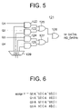
- FIG. 5 is a block diagram of the selector shown in FIG. 1 .
- FIG. 6 is an example of the description in HDL for the selector of FIG. 5 .
- FIG. 7 is a block diagram of a conventional register file.
- FIG. 8 is an example of design description of the multiplexer used in the output port selector shown in FIG. 7 .
- FIG. 9 is a block diagram of the 2-input/1-output multiplexer stored in the cell library with a gate level notation.
- FIG. 10 is a block diagram of the 4-input/1-output multiplexer including the multiplexers shown in FIG. 9 .
- FIG. 11 is a circuit diagram of a synchronous D-FF employed in the memory of the conventional register file.
- the selection signal generator 110 includes therein decoders DECj and AND circuits ANDj, which are respectively provided in number corresponding to the number of write ports WR_DATAj, and an activating signal generator 111 .
- Each decoder DECj decodes the write address WR_ADRSj to generate an address signal having bits in number corresponding to the number of registers, wherein only one of the bits assumes “1”,
- Each decoder DECj decodes a corresponding 2-bit write address signal WR_ADRS j, for example, address (01), to generate a 4-bit signal (0010) for selecting one of the registers Fi, i.e., register F 1 .
- Each AND circuit ANDj includes AND gates ANDij in number corresponding to the number of registers Fi, generates a logical product of each bit of the output from the decoder DECj and a write enable signal WR_ENj from the processor core, and delivers the logical product as a selection signal Sij to the registers F 0 to F 3 .
- the activating signal generator 111 includes OR gates in number corresponding to the number of registers Fi, wherein each OR gate corresponding to one of the registers Fi generates a logical sum of the outputs, Sij, from the AND circuits AND 0 to AND 3 corresponding to the one of the registers Fi, and delivers the same as an activating signal ⁇ i to the one of the registers Fi selected by the write address signal WR_ADRSj.
- the activating signal generator 111 delivers the logical sum as an activating signal ⁇ i to the register F 1 .
- Each register Fi includes an input port selector 130 and a data storage 140 .
- FIG. 3 there is shown the detail of a configuration of the register F 0 .
- Other registers are similar to the register F 0 shown therein.
- the input port selector 130 receives write data through the write ports WR_DATAj and stores the same in the data storage 140 based on the selection signal Sij supplied from the selection signal generator 110 .
- the data storage 140 includes memory memories 141 in number corresponding to the number of bits to be stored and corresponding clock gates 142 , and delivers data Qi. The number between the parentheses in FIG. 3 shows the sequential order of the bits of the write data.
- the input port selector 130 includes, for each bit of the write data, AND gates 131 to 134 and an OR gate 135 .
- Each AND gate 131 generates a logical sum of the selection signal S 00 and a corresponding bit of the write data supplied through the write port WR_DATA 0 .
- Each AND gate 132 generates a logical sum of the inverted signal of the selection signal S 00 , selection signal S 01 and a corresponding bit of the write data supplied through the write port WR_DATAl.
- Each AND gate 133 generates a logical sum of the inverted signal of the selection signal S 00 , inverted signal of the selection signal S 01 , the selection signal S 02 , and a corresponding bit of the write data supplied through the write port WR_DATA 2 .
- Each AND gate 134 generates a logical sum of the inverted signal of the selection signal S 00 , inverted signal of the selection signal S 01 , inverted signal of the selection signal S 02 , the selection signal S 03 and a corresponding bit of the write data supplied through the write port WR_DATA 3 .
- Each OR gate 135 generates a logical sum of the outputs from the AND gates 131 to 134 to deliver the same to the data storage 140 .
- the input port selector 130 is implemented by a selector having a priority order among the input port selectors 130 , similarly to the input/output port selector 230 in the conventional register file 200 shown in FIG. 7 . For example, if the selection signal S 00 assumes a high level, data from the write port WR_DATA 0 is delivered via the OR gate 135 to the data storage 140 due to the output from the AND gates 132 to 134 being fixed at a low level.
- the memory 141 includes synchronous D-FFs in number corresponding to the number of bits of data to be stored in the register Fi. Each D-FF receives and stores data from the write port WR_DATAj in a bit-by-bit basis, in synchrony with the clock signal CLK supplied through the clock gate 142 .
- the clock gate 142 shown in FIG. 3 includes a latch circuit 143 and an AND gate 144 .
- FIG. 4B shows the timing chart of the clock gate 142 of FIG. 4A .
- the latch circuit 143 latches the activating signal ⁇ i at the falling edge of the clock signal CLK, as shown in FIG. 4B , to deliver the latched activating signal ⁇ i.
- the AND gate 144 generates a logical product of the clock signal CLK and the latched activating signal ⁇ i, whereby the clock gate 142 delivers the clock signal CLK to the corresponding memory 141 during the high level of the latched activating signal ⁇ i.
- the input port selector 130 receives at the data input thereof data from the write port WR_DATAJ specified.
- the clock input and the data input of each D-FF are fixed at a low level, whereby the data stored in each D-FF is not updated.
- the output port selector block (read data selector block) 120 includes therein selectors 121 in number corresponding to the number of the read ports RD_DATAk, and has a function similar to the function of the output port selector 220 in the conventional register file 200 shown in FIG. 7 .
- Each selector 121 receives data Qi stored in the register Fi, similarly to the multiplexer MUX in the output port selector 220 , to select data Qi to be read out through the read port RD_DATAk based on the read address RD_ADRSk.
- each selector 121 includes therein AND gates 122 to 125 in number corresponding to the number of bits of data to be stored in the register Fi, corresponding OR gates 126 to 128 and a decoder 129 .
- the decoder 129 generates an activating signal which activates one of the output signal lines corresponding to the registers Fi based on the read address RD_ADRSk, thereby selecting one of the registers Fi from which the read port RD_ADRSk is to read the data. If the 2-bit address specifies (01), for example, the decoder delivers a 4-bit signal (0010) for selecting one of the registers Fi, i.e., F 1 .
- Each of the AND gates 122 to 125 generates a logical product of the data Qi from the register Fi and the output from the corresponding decoder 129 to deliver the same to the OR gate 126 or 127 . Since only one of the signals delivered from the decoders 129 assumes a high level, the outputs of the AND gates 122 to 125 are fixed at a low level except the AND gate receiving the high level.
- the first-stage OR gates 126 and 127 generate a logical product of outputs from the AND gates 122 and 123 and a logical product of outputs from the AND gates 124 and 125 , respectively, and the second-stage OR gate 128 generates a logical product of outputs from the OR gates 126 and 127 .
- the AND gate 122 receives a high-level data from the decoder 129 in the selector 121 corresponding to the read port RA_DATA 0 .
- data Q 0 (0) assumes “0” or a low level
- all the outputs from the AND gates 122 to 125 assume “0”, whereby the read port RD_DATA 0 delivers therethrough “0” of data Q 0 (0).
- the decoder 129 delivers a high-level signal to the AND gate 125 , the output from the AND gate 125 as well as the outputs from the OR gates 127 and 128 shifts from “0” to “1”, whereby the read port RD_DATA 0 delivers therethrough “1” as data Q 3 (0).
- FIG. 6 exemplifies design description of the selector 121 .
- This description describes the function of the selector 121 by using a logical sum and a logical product, which is different from the multiplexer in the conventional description (in FIG. 8 ) using a case sentence.
- “&” corresponds to a logical product which is to be implemented by hardware
- ” corresponds to a logical sum which is to be implemented by hardware.
- the selector 121 is described by combination of the logic gates so that the function of the multiplexer is not implemented by using the primitive cells prepared in the cell library for a multiplexer.
- the gate level circuit for the selector 121 is configured by the combination of the logic gates, such as AND or OR gates without depending on the tool for the logical synthesis and the cell library used in the design.
- the selector 121 used in the present embodiment includes an additional decoder 129 , as described above, which consumes some amount of current upon a change of the read address RD_ADRSk, the single decoder 129 can be used in common for all the bits of data Qi in the register Fi, whereby both the circuit scale and the operating current of the decoder 129 remain within a moderate increase.
- the increase of the operating current due to the provision of the decoder 129 is significantly lower compared to the dissipated current of the multiplexer in the conventional register file shown in FIG. 9 , which wastes the electric power upon the change of the multiplexer.
- the outputs from the AND gates 122 to 125 which receive non-selection data do not dissipate the operating current, whereby the current dissipation is reduced in the present embodiment.
- the input port selector 30 having a priority order is configured by a combinational circuit including AND gates and OR gates.
- the input port selector 130 allows the input of the memory 141 to be fixed at a low level when the write data is not to be stored in the memory 141 . This prevents operation of the master latch in the D-FF of the data storage to thereby save the power dissipation as encountered in the data storage of the conventional register file.
- the function of the selector 121 is described by the combination of the AND gates and OR gates so as not to use the primitive cells for a multiplexer stored in the library cell. This allows the gate-level circuit configuration of the selector 121 to be implemented by the combinational circuit without depending on the tool for the logical synthesis or cell library.
- the principle of the design method of the present invention should be also applied to the design of the input port selector 130 in each register Fi.
- the number of registers, bit length of the data stored in the registers, number of write ports, number of read ports etc. employed in the present embodiment are mere examples, and these numbers etc. may be selected depending on the specification of the semiconductor device to be designed. In such a case, the write address and read address have bit lengths determined based on the number of ports.
Landscapes
- Engineering & Computer Science (AREA)
- Theoretical Computer Science (AREA)
- Software Systems (AREA)
- Physics & Mathematics (AREA)
- General Engineering & Computer Science (AREA)
- General Physics & Mathematics (AREA)
- Logic Circuits (AREA)
- Design And Manufacture Of Integrated Circuits (AREA)
Abstract
Description
Claims (4)
Applications Claiming Priority (2)
| Application Number | Priority Date | Filing Date | Title |
|---|---|---|---|
| JP2002265521A JP2004102799A (en) | 2002-09-11 | 2002-09-11 | Register file and method for designing register file |
| JP2002-265521 | 2002-09-11 |
Publications (2)
| Publication Number | Publication Date |
|---|---|
| US20040060015A1 US20040060015A1 (en) | 2004-03-25 |
| US7313768B2 true US7313768B2 (en) | 2007-12-25 |
Family
ID=29244339
Family Applications (1)
| Application Number | Title | Priority Date | Filing Date |
|---|---|---|---|
| US10/658,202 Expired - Fee Related US7313768B2 (en) | 2002-09-11 | 2003-09-10 | Register file and method for designing a register file |
Country Status (6)
| Country | Link |
|---|---|
| US (1) | US7313768B2 (en) |
| JP (1) | JP2004102799A (en) |
| KR (1) | KR100613030B1 (en) |
| CN (1) | CN1501292A (en) |
| GB (1) | GB2394581B (en) |
| TW (1) | TW200414032A (en) |
Cited By (4)
| Publication number | Priority date | Publication date | Assignee | Title |
|---|---|---|---|---|
| US20090213981A1 (en) * | 2005-02-08 | 2009-08-27 | Nxp B.V. | Low-power register array for fast shift operations |
| US9786350B2 (en) | 2013-03-18 | 2017-10-10 | Semiconductor Energy Laboratory Co., Ltd. | Memory device |
| US9799379B2 (en) | 2012-07-20 | 2017-10-24 | Nxp Usa, Inc. | Hold time aware register file module and method therefor |
| US10867645B2 (en) | 2018-04-05 | 2020-12-15 | Samsung Electronics Co., Ltd. | Memory device including plurality of latches and system on chip including the same |
Families Citing this family (20)
| Publication number | Priority date | Publication date | Assignee | Title |
|---|---|---|---|---|
| US7183825B2 (en) * | 2004-04-06 | 2007-02-27 | Freescale Semiconductor, Inc. | State retention within a data processing system |
| CN1333356C (en) * | 2004-07-23 | 2007-08-22 | 中国人民解放军国防科学技术大学 | Write serialization and resource duplication combined multi-port register file design method |
| US8447931B1 (en) | 2004-08-27 | 2013-05-21 | Oracle America, Inc. | Processor with a register file that supports multiple-issue execution |
| US7647481B2 (en) * | 2005-02-25 | 2010-01-12 | Qualcomm Incorporated | Reducing power by shutting down portions of a stacked register file |
| US7610571B2 (en) * | 2006-04-14 | 2009-10-27 | Cadence Design Systems, Inc. | Method and system for simulating state retention of an RTL design |
| WO2010025074A1 (en) * | 2008-08-28 | 2010-03-04 | Sandbridge Technologies, Inc. | Latch-based implementation of a register file for a multi-threaded processor |
| US8583897B2 (en) * | 2009-02-02 | 2013-11-12 | Arm Limited | Register file with circuitry for setting register entries to a predetermined value |
| US8331133B2 (en) * | 2009-06-26 | 2012-12-11 | Intel Corporation | Apparatuses for register file with novel bit cell implementation |
| CN101620524B (en) * | 2009-07-03 | 2011-08-10 | 中国人民解放军国防科学技术大学 | Matrix register file for supporting whole reading and writing operations of matrix |
| EP2566050A4 (en) | 2010-04-30 | 2014-05-14 | Murata Manufacturing Co | COMPOSITE COMPONENT |
| US8972961B2 (en) * | 2010-05-19 | 2015-03-03 | International Business Machines Corporation | Instruction scheduling approach to improve processor performance |
| CN102176138B (en) * | 2011-03-01 | 2013-04-03 | 上海维宏电子科技股份有限公司 | Hardware port targeted management control method for numerical control system |
| GB2501791B (en) | 2013-01-24 | 2014-06-11 | Imagination Tech Ltd | Register file having a plurality of sub-register files |
| CN108182955B (en) * | 2018-01-29 | 2020-09-25 | 中国人民解放军国防科技大学 | A low-latency write priority decoding circuit |
| CN113721979A (en) * | 2020-05-25 | 2021-11-30 | 北京希姆计算科技有限公司 | Register circuit capable of configuring bit width, method, decoding circuit and chip |
| GB2597077B (en) * | 2020-07-14 | 2022-07-27 | Graphcore Ltd | Clearing register data |
| CN113470554B (en) * | 2021-07-15 | 2023-08-29 | 中科芯集成电路有限公司 | Open circuit detection readback method for LED display driving chip |
| CN115691610B (en) * | 2022-10-31 | 2025-09-09 | 山东华芯半导体有限公司 | SRAM access device for realizing SSD master control RAID |
| EP4418108B1 (en) * | 2023-02-13 | 2025-10-01 | STMicroelectronics International N.V. | Improved register bank for electronic processor and initialization method of the register bank |
| CN120014957B (en) * | 2025-04-14 | 2025-07-18 | 江苏帝奥微电子股份有限公司 | A panel gate drive circuit based on LTPS CMOS |
Citations (16)
| Publication number | Priority date | Publication date | Assignee | Title |
|---|---|---|---|---|
| JPS59106021A (en) | 1982-12-10 | 1984-06-19 | Oki Electric Ind Co Ltd | Bus constituting system |
| SU1128253A1 (en) | 1982-01-14 | 1984-12-07 | Предприятие П/Я В-2969 | Device for generating addresses of register storage |
| JPH02277125A (en) | 1989-01-13 | 1990-11-13 | Toshiba Corp | Register bank circuit |
| JPH05206791A (en) | 1992-01-29 | 1993-08-13 | Nec Ic Microcomput Syst Ltd | D type flip-flop |
| JPH0738398A (en) | 1993-07-15 | 1995-02-07 | Nec Corp | Clock switching circuit |
| JPH07262003A (en) | 1994-03-18 | 1995-10-13 | Hitachi Ltd | Register access controller |
| US5657291A (en) * | 1996-04-30 | 1997-08-12 | Sun Microsystems, Inc. | Multiport register file memory cell configuration for read operation |
| US5815023A (en) | 1997-03-20 | 1998-09-29 | Sun Microsystems, Inc. | Unbalanced multiplexer and arbiter combination |
| US6219756B1 (en) * | 1997-12-24 | 2001-04-17 | Fujitsu Limited | Rapidly-readable register file |
| US6320813B1 (en) * | 2000-03-02 | 2001-11-20 | Sun Microsystems, Inc. | Decoding of a register file |
| US6556501B1 (en) * | 1998-04-28 | 2003-04-29 | Hewlett-Packard Company | Multi-port computer register file having shared word lines for read and write ports and storage elements that power down or enter a high-impendance state during write operations |
| US6594714B1 (en) * | 2000-05-01 | 2003-07-15 | Hewlett-Packard Development Company, L.P. | Reconfigurable FIFO interface to support multiple channels in bundled agent configurations |
| US6654870B1 (en) * | 1999-06-21 | 2003-11-25 | Pts Corporation | Methods and apparatus for establishing port priority functions in a VLIW processor |
| US6766433B2 (en) * | 2001-09-21 | 2004-07-20 | Freescale Semiconductor, Inc. | System having user programmable addressing modes and method therefor |
| US6826110B2 (en) * | 2002-10-17 | 2004-11-30 | International Business Machines Corporation | Cell circuit for multiport memory using decoder |
| US6831850B2 (en) * | 2000-06-08 | 2004-12-14 | Netlogic Microsystems, Inc. | Content addressable memory with configurable class-based storage partition |
-
2002
- 2002-09-11 JP JP2002265521A patent/JP2004102799A/en active Pending
-
2003
- 2003-09-09 KR KR1020030062914A patent/KR100613030B1/en not_active Expired - Fee Related
- 2003-09-10 US US10/658,202 patent/US7313768B2/en not_active Expired - Fee Related
- 2003-09-10 TW TW092125005A patent/TW200414032A/en unknown
- 2003-09-10 GB GB0321211A patent/GB2394581B/en not_active Expired - Fee Related
- 2003-09-11 CN CNA031581234A patent/CN1501292A/en active Pending
Patent Citations (17)
| Publication number | Priority date | Publication date | Assignee | Title |
|---|---|---|---|---|
| SU1128253A1 (en) | 1982-01-14 | 1984-12-07 | Предприятие П/Я В-2969 | Device for generating addresses of register storage |
| JPS59106021A (en) | 1982-12-10 | 1984-06-19 | Oki Electric Ind Co Ltd | Bus constituting system |
| JPH02277125A (en) | 1989-01-13 | 1990-11-13 | Toshiba Corp | Register bank circuit |
| JPH05206791A (en) | 1992-01-29 | 1993-08-13 | Nec Ic Microcomput Syst Ltd | D type flip-flop |
| JPH0738398A (en) | 1993-07-15 | 1995-02-07 | Nec Corp | Clock switching circuit |
| JPH07262003A (en) | 1994-03-18 | 1995-10-13 | Hitachi Ltd | Register access controller |
| US5657291A (en) * | 1996-04-30 | 1997-08-12 | Sun Microsystems, Inc. | Multiport register file memory cell configuration for read operation |
| JPH10275075A (en) | 1997-03-20 | 1998-10-13 | Sun Microsyst Inc | Combination of unbalanced multiplexer and arbiter |
| US5815023A (en) | 1997-03-20 | 1998-09-29 | Sun Microsystems, Inc. | Unbalanced multiplexer and arbiter combination |
| US6219756B1 (en) * | 1997-12-24 | 2001-04-17 | Fujitsu Limited | Rapidly-readable register file |
| US6556501B1 (en) * | 1998-04-28 | 2003-04-29 | Hewlett-Packard Company | Multi-port computer register file having shared word lines for read and write ports and storage elements that power down or enter a high-impendance state during write operations |
| US6654870B1 (en) * | 1999-06-21 | 2003-11-25 | Pts Corporation | Methods and apparatus for establishing port priority functions in a VLIW processor |
| US6320813B1 (en) * | 2000-03-02 | 2001-11-20 | Sun Microsystems, Inc. | Decoding of a register file |
| US6594714B1 (en) * | 2000-05-01 | 2003-07-15 | Hewlett-Packard Development Company, L.P. | Reconfigurable FIFO interface to support multiple channels in bundled agent configurations |
| US6831850B2 (en) * | 2000-06-08 | 2004-12-14 | Netlogic Microsystems, Inc. | Content addressable memory with configurable class-based storage partition |
| US6766433B2 (en) * | 2001-09-21 | 2004-07-20 | Freescale Semiconductor, Inc. | System having user programmable addressing modes and method therefor |
| US6826110B2 (en) * | 2002-10-17 | 2004-11-30 | International Business Machines Corporation | Cell circuit for multiport memory using decoder |
Non-Patent Citations (3)
| Title |
|---|
| J. L. Hennessy et al., "Computer Organization & Design," 1996, (translated by Mitsuaki Narita); ISBN 4-8222-8002-0, pp. 678-680, Nikkei BP Corp. |
| Japanese Office Action dated Oct. 1, 2007, Japanese Patent Office, Application No. 2002-265521. |
| John L. Hennessy, B.5 Memory Elements, Computer Organization and Design 2<SUP>nd </SUP>Edition (vol. 2), Japan, Nikkei Business Publications, Inc., Hisashi Okamura, May 17, 1999, 2<SUP>nd </SUP>Edition, pp. 799-804. |
Cited By (5)
| Publication number | Priority date | Publication date | Assignee | Title |
|---|---|---|---|---|
| US20090213981A1 (en) * | 2005-02-08 | 2009-08-27 | Nxp B.V. | Low-power register array for fast shift operations |
| US9799379B2 (en) | 2012-07-20 | 2017-10-24 | Nxp Usa, Inc. | Hold time aware register file module and method therefor |
| US9786350B2 (en) | 2013-03-18 | 2017-10-10 | Semiconductor Energy Laboratory Co., Ltd. | Memory device |
| US10867645B2 (en) | 2018-04-05 | 2020-12-15 | Samsung Electronics Co., Ltd. | Memory device including plurality of latches and system on chip including the same |
| US11289138B2 (en) | 2018-04-05 | 2022-03-29 | Samsung Electronics Co., Ltd. | Memory device including plurality of latches and system on chip including the same |
Also Published As
| Publication number | Publication date |
|---|---|
| KR100613030B1 (en) | 2006-08-16 |
| TW200414032A (en) | 2004-08-01 |
| GB2394581A (en) | 2004-04-28 |
| US20040060015A1 (en) | 2004-03-25 |
| KR20040023762A (en) | 2004-03-18 |
| JP2004102799A (en) | 2004-04-02 |
| CN1501292A (en) | 2004-06-02 |
| GB0321211D0 (en) | 2003-10-08 |
| GB2394581B (en) | 2005-12-14 |
Similar Documents
| Publication | Publication Date | Title |
|---|---|---|
| US7313768B2 (en) | Register file and method for designing a register file | |
| US9053274B1 (en) | Register retiming technique | |
| US9069920B2 (en) | Automated circuit design | |
| JP3150122B2 (en) | Limited register sharing method and system for low power VLSI design | |
| CN101751980B (en) | Embedded programmable memory based on memory IP core | |
| US20070283311A1 (en) | Method and system for dynamic reconfiguration of field programmable gate arrays | |
| US20040145942A1 (en) | Reconfigurable logic device | |
| US8132144B2 (en) | Automatic clock-gating insertion and propagation technique | |
| JP5985900B2 (en) | Behavioral synthesis device, data processing system including behavioral synthesis device, and behavioral synthesis program | |
| US7752592B2 (en) | Scheduler design to optimize system performance using configurable acceleration engines | |
| US8161435B2 (en) | Reset mechanism conversion | |
| US20120311009A1 (en) | Hybrid adder using dynamic and static circuits | |
| US20040236929A1 (en) | Logic circuit and program for executing thereon | |
| JP2000187676A (en) | Logic synthesis device and computer-readable recording medium storing logic synthesis program | |
| US7844937B2 (en) | Method and apparatus for making a semiconductor device using hardware description having merged functional and test logic blocks | |
| US7769929B1 (en) | Design tool selection and implementation of port adapters | |
| US20050154577A1 (en) | Method and apparatus for emulation of logic circuits | |
| US20220200603A1 (en) | Direct bi-directional gray code counter | |
| CN115952759B (en) | FPGA layout method, device, electronic device and storage medium | |
| Jozwiak et al. | Hardware synthesis for reconfigurable heterogeneous pipelined accelerators | |
| Tatas et al. | FPGA architecture design and toolset for logic implementation | |
| Dalal et al. | An 8 bit Power-Efficient MIPS Processor | |
| Chonnad et al. | Verilog: Frequently Asked Questions: Language, Applications and Extensions | |
| Pitkänen et al. | Parallel memory architecture for application-specific instruction-set processors | |
| Gorski et al. | The FPOA, a Medium-grained Reconfigurable Architecture for High-level Synthesis |
Legal Events
| Date | Code | Title | Description |
|---|---|---|---|
| AS | Assignment |
Owner name: NEC ELECTRONICS CORPORATION, JAPAN Free format text: ASSIGNMENT OF ASSIGNORS INTEREST;ASSIGNOR:MOCHIZUKI, AKIRA;REEL/FRAME:014480/0901 Effective date: 20030908 |
|
| FEPP | Fee payment procedure |
Free format text: PAYOR NUMBER ASSIGNED (ORIGINAL EVENT CODE: ASPN); ENTITY STATUS OF PATENT OWNER: LARGE ENTITY |
|
| STCF | Information on status: patent grant |
Free format text: PATENTED CASE |
|
| AS | Assignment |
Owner name: RENESAS ELECTRONICS CORPORATION, JAPAN Free format text: CHANGE OF NAME;ASSIGNOR:NEC ELECTRONICS CORPORATION;REEL/FRAME:025525/0136 Effective date: 20100401 |
|
| FPAY | Fee payment |
Year of fee payment: 4 |
|
| FPAY | Fee payment |
Year of fee payment: 8 |
|
| AS | Assignment |
Owner name: RENESAS ELECTRONICS CORPORATION, JAPAN Free format text: CHANGE OF ADDRESS;ASSIGNOR:RENESAS ELECTRONICS CORPORATION;REEL/FRAME:044928/0001 Effective date: 20150806 |
|
| FEPP | Fee payment procedure |
Free format text: MAINTENANCE FEE REMINDER MAILED (ORIGINAL EVENT CODE: REM.); ENTITY STATUS OF PATENT OWNER: LARGE ENTITY |
|
| LAPS | Lapse for failure to pay maintenance fees |
Free format text: PATENT EXPIRED FOR FAILURE TO PAY MAINTENANCE FEES (ORIGINAL EVENT CODE: EXP.); ENTITY STATUS OF PATENT OWNER: LARGE ENTITY |
|
| STCH | Information on status: patent discontinuation |
Free format text: PATENT EXPIRED DUE TO NONPAYMENT OF MAINTENANCE FEES UNDER 37 CFR 1.362 |
|
| FP | Lapsed due to failure to pay maintenance fee |
Effective date: 20191225 |