US7299528B2 - Method for forming a multi-frequency surface acoustic wave device - Google Patents
Method for forming a multi-frequency surface acoustic wave device Download PDFInfo
- Publication number
- US7299528B2 US7299528B2 US10/288,529 US28852902A US7299528B2 US 7299528 B2 US7299528 B2 US 7299528B2 US 28852902 A US28852902 A US 28852902A US 7299528 B2 US7299528 B2 US 7299528B2
- Authority
- US
- United States
- Prior art keywords
- forming
- layer
- conductive
- conductive film
- resist layer
- Prior art date
- Legal status (The legal status is an assumption and is not a legal conclusion. Google has not performed a legal analysis and makes no representation as to the accuracy of the status listed.)
- Expired - Lifetime, expires
Links
- 238000010897 surface acoustic wave method Methods 0.000 title claims abstract description 59
- 238000000034 method Methods 0.000 title claims abstract description 54
- 239000000758 substrate Substances 0.000 claims abstract description 41
- 238000004519 manufacturing process Methods 0.000 claims abstract description 5
- 239000000463 material Substances 0.000 claims description 31
- 238000000151 deposition Methods 0.000 claims description 7
- 229910052719 titanium Inorganic materials 0.000 claims description 6
- 229910052782 aluminium Inorganic materials 0.000 claims description 5
- 239000004020 conductor Substances 0.000 claims description 5
- 238000005530 etching Methods 0.000 claims description 3
- 239000004065 semiconductor Substances 0.000 claims description 3
- 229910003327 LiNbO3 Inorganic materials 0.000 claims description 2
- 229910012463 LiTaO3 Inorganic materials 0.000 claims description 2
- 229910020289 Pb(ZrxTi1-x)O3 Inorganic materials 0.000 claims description 2
- 229910020273 Pb(ZrxTi1−x)O3 Inorganic materials 0.000 claims description 2
- 229910052802 copper Inorganic materials 0.000 claims description 2
- 239000013078 crystal Substances 0.000 claims description 2
- 229910052759 nickel Inorganic materials 0.000 claims description 2
- 229910052721 tungsten Inorganic materials 0.000 claims description 2
- 150000001875 compounds Chemical class 0.000 claims 2
- 229910011129 Li2B407 Inorganic materials 0.000 claims 1
- 239000000919 ceramic Substances 0.000 claims 1
- 239000010936 titanium Substances 0.000 description 6
- RTAQQCXQSZGOHL-UHFFFAOYSA-N Titanium Chemical compound [Ti] RTAQQCXQSZGOHL-UHFFFAOYSA-N 0.000 description 5
- XAGFODPZIPBFFR-UHFFFAOYSA-N aluminium Chemical compound [Al] XAGFODPZIPBFFR-UHFFFAOYSA-N 0.000 description 4
- 230000009977 dual effect Effects 0.000 description 4
- PXHVJJICTQNCMI-UHFFFAOYSA-N Nickel Chemical compound [Ni] PXHVJJICTQNCMI-UHFFFAOYSA-N 0.000 description 3
- 239000011651 chromium Substances 0.000 description 3
- 238000000059 patterning Methods 0.000 description 3
- VYZAMTAEIAYCRO-UHFFFAOYSA-N Chromium Chemical compound [Cr] VYZAMTAEIAYCRO-UHFFFAOYSA-N 0.000 description 2
- 230000015572 biosynthetic process Effects 0.000 description 2
- 229910052804 chromium Inorganic materials 0.000 description 2
- 239000010949 copper Substances 0.000 description 2
- 230000008021 deposition Effects 0.000 description 2
- 230000000694 effects Effects 0.000 description 2
- 229920002120 photoresistant polymer Polymers 0.000 description 2
- 238000012876 topography Methods 0.000 description 2
- RYGMFSIKBFXOCR-UHFFFAOYSA-N Copper Chemical compound [Cu] RYGMFSIKBFXOCR-UHFFFAOYSA-N 0.000 description 1
- 229910011131 Li2B4O7 Inorganic materials 0.000 description 1
- NRTOMJZYCJJWKI-UHFFFAOYSA-N Titanium nitride Chemical compound [Ti]#N NRTOMJZYCJJWKI-UHFFFAOYSA-N 0.000 description 1
- 238000010420 art technique Methods 0.000 description 1
- 229910010293 ceramic material Inorganic materials 0.000 description 1
- 238000005229 chemical vapour deposition Methods 0.000 description 1
- 230000001419 dependent effect Effects 0.000 description 1
- 238000001514 detection method Methods 0.000 description 1
- 238000009713 electroplating Methods 0.000 description 1
- 230000005284 excitation Effects 0.000 description 1
- 238000005240 physical vapour deposition Methods 0.000 description 1
- 230000001902 propagating effect Effects 0.000 description 1
- 229910052710 silicon Inorganic materials 0.000 description 1
- 239000010703 silicon Substances 0.000 description 1
- WFKWXMTUELFFGS-UHFFFAOYSA-N tungsten Chemical compound [W] WFKWXMTUELFFGS-UHFFFAOYSA-N 0.000 description 1
- 239000010937 tungsten Substances 0.000 description 1
Images


Classifications
-
- H—ELECTRICITY
- H03—ELECTRONIC CIRCUITRY
- H03H—IMPEDANCE NETWORKS, e.g. RESONANT CIRCUITS; RESONATORS
- H03H9/00—Networks comprising electromechanical or electro-acoustic devices; Electromechanical resonators
- H03H9/02—Details
- H03H9/125—Driving means, e.g. electrodes, coils
- H03H9/145—Driving means, e.g. electrodes, coils for networks using surface acoustic waves
- H03H9/14538—Formation
-
- H—ELECTRICITY
- H03—ELECTRONIC CIRCUITRY
- H03H—IMPEDANCE NETWORKS, e.g. RESONANT CIRCUITS; RESONATORS
- H03H3/00—Apparatus or processes specially adapted for the manufacture of impedance networks, resonating circuits, resonators
- H03H3/007—Apparatus or processes specially adapted for the manufacture of impedance networks, resonating circuits, resonators for the manufacture of electromechanical resonators or networks
- H03H3/08—Apparatus or processes specially adapted for the manufacture of impedance networks, resonating circuits, resonators for the manufacture of electromechanical resonators or networks for the manufacture of resonators or networks using surface acoustic waves
-
- H—ELECTRICITY
- H05—ELECTRIC TECHNIQUES NOT OTHERWISE PROVIDED FOR
- H05K—PRINTED CIRCUITS; CASINGS OR CONSTRUCTIONAL DETAILS OF ELECTRIC APPARATUS; MANUFACTURE OF ASSEMBLAGES OF ELECTRICAL COMPONENTS
- H05K3/00—Apparatus or processes for manufacturing printed circuits
- H05K3/02—Apparatus or processes for manufacturing printed circuits in which the conductive material is applied to the surface of the insulating support and is thereafter removed from such areas of the surface which are not intended for current conducting or shielding
- H05K3/04—Apparatus or processes for manufacturing printed circuits in which the conductive material is applied to the surface of the insulating support and is thereafter removed from such areas of the surface which are not intended for current conducting or shielding the conductive material being removed mechanically, e.g. by punching
- H05K3/046—Apparatus or processes for manufacturing printed circuits in which the conductive material is applied to the surface of the insulating support and is thereafter removed from such areas of the surface which are not intended for current conducting or shielding the conductive material being removed mechanically, e.g. by punching by selective transfer or selective detachment of a conductive layer
- H05K3/048—Apparatus or processes for manufacturing printed circuits in which the conductive material is applied to the surface of the insulating support and is thereafter removed from such areas of the surface which are not intended for current conducting or shielding the conductive material being removed mechanically, e.g. by punching by selective transfer or selective detachment of a conductive layer using a lift-off resist pattern or a release layer pattern
-
- Y—GENERAL TAGGING OF NEW TECHNOLOGICAL DEVELOPMENTS; GENERAL TAGGING OF CROSS-SECTIONAL TECHNOLOGIES SPANNING OVER SEVERAL SECTIONS OF THE IPC; TECHNICAL SUBJECTS COVERED BY FORMER USPC CROSS-REFERENCE ART COLLECTIONS [XRACs] AND DIGESTS
- Y10—TECHNICAL SUBJECTS COVERED BY FORMER USPC
- Y10T—TECHNICAL SUBJECTS COVERED BY FORMER US CLASSIFICATION
- Y10T29/00—Metal working
- Y10T29/42—Piezoelectric device making
-
- Y—GENERAL TAGGING OF NEW TECHNOLOGICAL DEVELOPMENTS; GENERAL TAGGING OF CROSS-SECTIONAL TECHNOLOGIES SPANNING OVER SEVERAL SECTIONS OF THE IPC; TECHNICAL SUBJECTS COVERED BY FORMER USPC CROSS-REFERENCE ART COLLECTIONS [XRACs] AND DIGESTS
- Y10—TECHNICAL SUBJECTS COVERED BY FORMER USPC
- Y10T—TECHNICAL SUBJECTS COVERED BY FORMER US CLASSIFICATION
- Y10T29/00—Metal working
- Y10T29/43—Electric condenser making
- Y10T29/435—Solid dielectric type
-
- Y—GENERAL TAGGING OF NEW TECHNOLOGICAL DEVELOPMENTS; GENERAL TAGGING OF CROSS-SECTIONAL TECHNOLOGIES SPANNING OVER SEVERAL SECTIONS OF THE IPC; TECHNICAL SUBJECTS COVERED BY FORMER USPC CROSS-REFERENCE ART COLLECTIONS [XRACs] AND DIGESTS
- Y10—TECHNICAL SUBJECTS COVERED BY FORMER USPC
- Y10T—TECHNICAL SUBJECTS COVERED BY FORMER US CLASSIFICATION
- Y10T29/00—Metal working
- Y10T29/49—Method of mechanical manufacture
- Y10T29/49002—Electrical device making
- Y10T29/49005—Acoustic transducer
-
- Y—GENERAL TAGGING OF NEW TECHNOLOGICAL DEVELOPMENTS; GENERAL TAGGING OF CROSS-SECTIONAL TECHNOLOGIES SPANNING OVER SEVERAL SECTIONS OF THE IPC; TECHNICAL SUBJECTS COVERED BY FORMER USPC CROSS-REFERENCE ART COLLECTIONS [XRACs] AND DIGESTS
- Y10—TECHNICAL SUBJECTS COVERED BY FORMER USPC
- Y10T—TECHNICAL SUBJECTS COVERED BY FORMER US CLASSIFICATION
- Y10T29/00—Metal working
- Y10T29/49—Method of mechanical manufacture
- Y10T29/49002—Electrical device making
- Y10T29/49007—Indicating transducer
-
- Y—GENERAL TAGGING OF NEW TECHNOLOGICAL DEVELOPMENTS; GENERAL TAGGING OF CROSS-SECTIONAL TECHNOLOGIES SPANNING OVER SEVERAL SECTIONS OF THE IPC; TECHNICAL SUBJECTS COVERED BY FORMER USPC CROSS-REFERENCE ART COLLECTIONS [XRACs] AND DIGESTS
- Y10—TECHNICAL SUBJECTS COVERED BY FORMER USPC
- Y10T—TECHNICAL SUBJECTS COVERED BY FORMER US CLASSIFICATION
- Y10T29/00—Metal working
- Y10T29/49—Method of mechanical manufacture
- Y10T29/49002—Electrical device making
- Y10T29/49117—Conductor or circuit manufacturing
- Y10T29/49124—On flat or curved insulated base, e.g., printed circuit, etc.
- Y10T29/4913—Assembling to base an electrical component, e.g., capacitor, etc.
-
- Y—GENERAL TAGGING OF NEW TECHNOLOGICAL DEVELOPMENTS; GENERAL TAGGING OF CROSS-SECTIONAL TECHNOLOGIES SPANNING OVER SEVERAL SECTIONS OF THE IPC; TECHNICAL SUBJECTS COVERED BY FORMER USPC CROSS-REFERENCE ART COLLECTIONS [XRACs] AND DIGESTS
- Y10—TECHNICAL SUBJECTS COVERED BY FORMER USPC
- Y10T—TECHNICAL SUBJECTS COVERED BY FORMER US CLASSIFICATION
- Y10T29/00—Metal working
- Y10T29/49—Method of mechanical manufacture
- Y10T29/49002—Electrical device making
- Y10T29/49117—Conductor or circuit manufacturing
- Y10T29/49124—On flat or curved insulated base, e.g., printed circuit, etc.
- Y10T29/49155—Manufacturing circuit on or in base
- Y10T29/49156—Manufacturing circuit on or in base with selective destruction of conductive paths
Definitions
- the present invention relates to integrated circuits. Specifically, the present invention is directed to a method for forming a surface acoustic wave (SAW) device.
- SAW surface acoustic wave
- a SAW device consists of coupled gratings that confine acoustic energy and leads to resonances, and of a coupled transducer that permits the excitation and detection of the acoustic waves.
- a typical structure of a SAW device 10 is shown in FIG. 1 .
- SAW device 10 includes reflector elements 12 and 14 and a filter element 16 disposed on a substrate 18 and connected together with one or more I/O pads 20 a and 20 b employing interconnects 22 a , 22 b and 22 c .
- Reflector elements 12 and 14 and filter element 16 produce a waveguiding effect on acoustic waves propagating therethrough, defining a plurality of waveguide elements.
- reflector element 12 includes a plurality of spaced-apart conductive elements 12 a extending parallel to each other.
- a first busbar 12 b is connected in common with one end of each of conductive elements 12 a
- a second busbar 12 c is connected in common with the ends of conductive elements 12 a disposed opposite to busbar 12 b .
- reflector element 14 includes a plurality of spaced-apart conductive elements 14 a , with a first busbar 14 b connected in common with one end thereof.
- a second busbar 14 c is connected in common with the ends of conductive elements 14 a disposed opposite to busbar 14 b.
- Filter element 16 includes first 16 a and second 16 b sets of conductive and spaced-apart interdigitated transducers (IDTs). An end of IDTs 16 a disposed opposite to IDTs 16 b is connected in common to busbar 16 c , and an end of TDTs 16 b disposed opposite to IDTs 16 a are connected in common to a busbar 16 d . Each of IDTs 16 a extends from busbar 16 c toward IDTs 16 b and terminates spaced-apart from busbar 16 d . Each of IDTs 16 b extends from busbar 16 d toward IDTs 16 a and terminates spaced-apart from busbar 16 c . The arrangement of IDTs 16 a and 16 b results in an IDT 16 a extending between adjacent IDTs 16 b and an IDT 16 b extending between adjacent IDTs 16 a.
- IDTs 16 a and 16 b results in an IDT 16 a extending between adjacent IDTs
- SAW device 10 may be controlled, inter alia, as a function of the thickness of conductive elements 12 a and 14 a , as well as IDTs 16 a and 16 b .
- SAW device 10 is also easily manufactured in a cost-effective manner employing standard semiconductor processing techniques. These factors combine to make SAW device 10 desirable for use as an RF band-pass filter in portable communication devices, such as mobile phones and portable computers. As a result, there are many prior art techniques directed toward forming SAW devices.
- U.S. Pat. No. 6,367,133 to Ikada et al. discloses, in pertinent part, a method of manufacturing a dual frequency surface acoustic wave apparatus.
- the apparatus includes first and second surface acoustic wave devices having different electrode film thicknesses on a common piezoelectric substrate.
- the method includes providing a piezoelectric substrate and forming a first conductive film on an entire surface of the piezoelectric substrate. A first resist layer is deposited over the entire surface of the first conductive film.
- the first resist layer is then patterned followed by a dry etch to form IDT electrodes of a first surface acoustic wave device, a short-circuit wiring electrode for establishing electrical connection between comb-shaped electrodes of the IDT electrodes, and a conductive film provided in a region including the entire area in which the second surface acoustic wave device is constructed. Thereafter, a wet etch is employed to remove the conductive film provided in the region including the entire area in which the second surface acoustic wave device is constructed. A second resist layer is then deposited on the entire surface of the piezoelectric substrate, and the substrate is then heated. In this manner, removed are portions of the second resist layer in superimposition with electrodes of the second surface acoustic wave device.
- a second conductive film having the same film thickness as the electrode film thickness of the second-surface acoustic wave device.
- a lift process is employed to remove the second resist layer and the second conductive film deposited on the second resist. This forms the electrodes of the second surface acoustic wave device, exposes the electrodes of the first surface acoustic wave device and disconnects the short-circuit wiring electrode in the first surface acoustic wave device.
- Publication No. 10-190390 discloses a method of manufacturing a surface acoustic wave apparatus in which a plurality of surface acoustic wave filter devices are disposed on a common piezoelectric substrate. To that end, a conductive film is formed on the piezoelectric substrate, and a resist is formed along the entire surface of the conductive film. Patterning of the resist is performed, forming a patterned resist layer. A dry etch process is employed to form electrodes of a first surface acoustic wave device. Thereafter, deposition of a second resist layer occurs, with a portion thereof not in superimposition with the first surface acoustic wave device being patterned, forming a patterned region in the second resist layer.
- a conductive film is deposited over the second resist layer, with a second acoustic wave device being formed in the patterned region thereof. Then a lift-off is performed leaving two sets of electrodes having differing thickness.
- the present invention provides a method of manufacturing a surface acoustic wave device on a piezoelectric substrate.
- the method features varying the resonant frequency of waveguide elements, such as interdigitated transducer electrodes (IDTs), by a single etch step that removes a sub-portion of multiple layers of conductive film disposed on the substrate.
- waveguide elements such as interdigitated transducer electrodes (IDTs)
- IDTs interdigitated transducer electrodes
- the resonant frequency of a subset of the plurality of waveguide elements is varied by removing one of the multiple layers associated with the subset.
- an additional resist layer is disposed atop of the multiple layers of conductive films and the resist layer.
- a sub-section of the additional resist layer is removed to expose a sub-section of the multiple layers of conductive film and one of the layers of the same is removed.
- a lift off technique is employed to remove all material present on the substrate, excepting material associated with the waveguide elements.
- FIG. 1 is a simplified plan view of a prior art surface acoustic wave (SAW) device
- FIG. 2 is a simplified plan view of a dual frequency SAW device that may be formed in accordance with the present invention
- FIG. 3 is a cross-sectional view showing a piezoelectric substrate with a first patterned resist layer disposed thereon to form a SAW device in accordance with a first method of the present invention
- FIG. 4 is a cross-sectional view of the structure shown in FIG. 3 with an adhesion film disposed thereon, in accordance with the first method of the present invention
- FIG. 5 is a cross-sectional view of the structure shown in FIG. 4 with a first conductive film disposed on the adhesion film, in accordance with the first method of the present invention
- FIG. 6 is a cross-sectional view of the structure shown in FIG. 5 with a second conductive film disposed on the first conductive film, in accordance with the first method of the present invention
- FIG. 7 is a cross-sectional view of the structure shown in FIG. 6 with a second resist layer disposed on the second conductive film, in accordance with the first method of the present invention
- FIG. 8 is a cross-sectional view of the structure shown in FIG. 7 with a sub-section of the second resist layer being removed to expose the sub-portion of the second conductive film in superimposition therewith, in accordance with the first method of the present invention
- FIG. 9 is a cross-sectional view of the structure shown in FIG. 8 with the sub-portion of the second conductive film being removed, exposing the first conductive film in superimposition with the sub-portion;
- FIG. 10 is a cross-sectional view of the structure shown in FIG. 9 after a lift-off technique to form a dual frequency SAW device, in accordance with the first method of the present invention
- FIG. 11 is a cross-sectional view showing a piezoelectric substrate with a second patterned resist layer disposed thereon to form a SAW device in accordance with a second method of the present invention
- FIG. 12 is a cross-sectional view of the structure shown in FIG. 11 with an adhesion film disposed thereon, in accordance with the second method of the present invention
- FIG. 13 is a cross-sectional view of the structure shown in FIG. 12 with a first conductive film disposed on the adhesion film, in accordance with the second method of the present invention
- FIG. 14 is a cross-sectional view of the structure shown in FIG. 13 with a cap film disposed on the conductive film, in accordance with the second method of the present invention
- FIG. 15 is a cross-sectional view of the structure shown in FIG. 14 with a second conductive film disposed on the cap film, in accordance with the second method of the present invention
- FIG. 16 is a cross-sectional view of the structure shown in FIG. 15 with a second resist layer disposed on the second conductive film, in accordance with the second method of the present invention
- FIG. 17 is a cross-sectional view of the structure shown in FIG. 16 with a sub-section of the second resist layer being removed to expose the sub-portion of the second conductive film in superimposition therewith, in accordance with the second method of the present invention
- FIG. 18 is a cross-sectional view of the structure shown in FIG. 17 with the sub-portion of the second conductive film being removed, exposing the cap film in superimposition therewith;
- FIG. 19 is a cross-sectional view of the structure shown in FIG. 18 after a lift-off technique to form a dual frequency SAW device, in accordance with the second method of the present invention.
- a multi-frequency SAW device 30 in accordance with the present invention includes first 32 and second 34 SAW circuits.
- SAW circuit 32 includes a plurality of waveguide elements, such as a pair of reflector elements 32 a and 32 b with a filter element 32 c connected therebetween. Reflector elements 32 a and 32 b and filter element 32 c are electrically coupled as discussed above with respect to reflector elements 12 and 14 and filter element 16 , of FIG. 1 .
- SAW circuit 34 includes reflector elements 34 a and 34 b with a filter element 34 c connected therebetween that are electrically coupled in a similar fashion.
- the method to form multi-frequency SAW device 30 commences with depositing a resist layer 40 atop of a piezoelectric substrate 42 .
- Substrate 42 may be formed from any known piezoelectric material, such as piezoelectric single crystal material, piezoelectric ceramic material and the like. Exemplary materials from which substrate 42 may be formed include LiTaO 3 , LiNbO 3 , Li 2 B 4 O 7 , La 3 Ga 5 SiO 14 and Pb(Zr x Ti 1 ⁇ x )O 3 .
- substrate 42 may be a standard semiconductor substrate formed, for example, from silicon and coated with a layer of piezoelectric material.
- Resist layer 40 is patterned so as to have gaps 44 , 46 , 48 , 50 and 52 present therein, exposing portions 44 a , 46 a , 48 a , 50 a and 52 a of substrate 42 .
- Gaps 44 , 46 , 48 , 50 and 52 may have identical or differing dimensions provide portions 44 a , 46 a , 48 a , 50 a and 52 a with identical or differing surface areas.
- Any type of resist material may be employed such as positive photoresist, negative photoresist and the like.
- Resist layer 40 may be deposited using known techniques, e.g., spin-on techniques.
- an adhesion layer 54 is deposited to cover resist layer 40 and portions 44 a , 46 a , 48 a , 50 a and 52 a of substrate 42 .
- the material from which adhesion layer 54 is formed facilitates desired adhesion between substrate 42 and a conductive film 56 formed adjacent thereto.
- conductive film 56 may be formed from any type of conductive material
- adhesion layer 54 may be formed from any material suitable to facilitate adhesion between conductive film 56 and substrate 42 .
- conductive film 56 may be formed from titanium (Ti), aluminum (Al), nickel (Ni), tungsten (W) and copper (Cu), and adhesion layer 54 may be formed from any of the aforementioned materials, as well as titanium nitride (TiN) and/or chromium (Cr).
- adhesion layer 54 is formed from titanium and conductive film 56 is formed from aluminum.
- the thickness of adhesion layer 54 is selected to have minimal effect on the desired operational frequencies of the resulting SAW device.
- adhesion layer 54 has a thickness in a range of 20–50 angstroms.
- the thickness of conductive film 56 is chosen to define the operational frequency of SAW circuit 32 , shown in FIG. 2 . Referring again to FIG.
- conductive film 56 has a thickness in a range of 1,500 to 2,500 angstroms. Both adhesion layer 54 and conductive film 56 may be deposited using any known deposition technique, such as, chemical vapor deposition, physical vapor deposition, electroplating and the like.
- a second conductive film 58 is formed atop of conductive film 56 .
- Conductive film 58 may be formed from material that is the same or different from the material from which conductive film 56 is formed.
- the thickness of conductive film 58 is selected to define the frequency of operation for SAW circuit 34 , shown in FIG. 2 , based upon the material employed to form second conductive film 58 and the presence of conductive film 56 .
- second conductive film 58 is formed from titanium material and has a thickness in a range of 500–1,100 angstroms.
- resist layer 60 is deposited to facilitate subsequent patterning and removal thereof so that a portion in superimposition with SAW circuit 34 remains while the portion in superimposition with SAW circuit 32 is removed.
- resist layer 60 may be deposited using any known process and to achieve any known topography.
- resist layer 60 is formed employing a spin-on process to completely cover second conductive film 58 and define a planar surface 62 . Thereafter, surface 62 is patterned so that a sub-section of resist layer 60 is developed away to expose a sub-portion of second conductive layer 58 in superimposition with a region 64 of substrate 42 in which SAW circuit 32 is formed.
- region 64 is exposed to an etch process, e.g., wet or dry etch processes, to remove the area of second conductive film 58 in superimposition with region 64 .
- the etch process varies the frequency associated with SAW circuit 32 , shown in FIG. 2 , so that the frequency is defined by the thickness of conductive film 56 in gap 46 , shown in FIG. 9 .
- a lift off technique is employed to remove all material from substrate 42 in superimposition with region 64 , excepting conductive film 56 and adhesion layer 54 disposed in gaps 44 , 46 and 48 .
- the lift off technique also removes all material from substrate 42 in superimposition with region 66 , excepting adhesion layer 54 , as well as first 56 and second 58 conductive films disposed in gaps 50 and 52 . In this manner, SAW circuits 32 and 34 are formed on substrate 42 , shown in FIG. 10 .
- the method to form multi-frequency SAW device 30 commences with deposition of a resist layer 140 atop of a piezoelectric substrate 142 , shown in FIG. 11 .
- portions of resist layer 140 are provided with gaps 144 , 146 , 148 , 150 and 152 present therein to expose portions 144 a , 146 a , 148 a , 150 a and 152 a of substrate 142 .
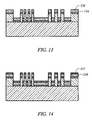
- an adhesion layer 154 is deposited to cover resist layer 140 and portions 144 a , 146 a , 148 a , 150 a and 152 a .
- a first conductive film 156 is deposited to cover adhesion layer 154 , shown in FIG. 13 .
- Adhesion layer 154 and first conductive film 156 may be formed from any suitable material.
- adhesion layer 154 is formed from titanium and first conductive film 156 is formed from aluminum having a thickness in a range of 1,500 to 2,500 angstroms.
- a cap layer 157 is deposited over first conductive film 156 .
- Cap layer 157 functions to prevent compromise of the structural integrity of first conductive film 156 when subjected to etchants.
- any suitable material may be employed to form cap layer 157 , dependent upon the etching chemistries.
- cap layer 157 is formed from titanium or chromium and has a thickness associated therewith that has minimal influence on the desired operational frequency of SAW circuits 32 and 34 , shown in FIG. 2 .
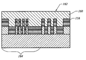
- a second conductive film 158 is formed atop of cap layer 157 .
- Conductive film 158 may be formed from material that is the same or different from the material from which conductive film 156 is formed. The thickness of conductive film 158 is selected to define the frequency of operation for SAW circuit 34 , shown in FIG. 2 , based upon the material employed to form second conductive film 158 , shown in FIG. 15 .
- second conductive film 158 is formed from aluminum (Al) and has a thickness in a range of 2,500 to 4,500 angstroms.
- second resist layer 160 formed atop of second conductive film 158 is a second resist layer 160 .
- Resist layer 160 is deposited to facilitate subsequent patterning and removal thereof so that a portion thereof remains in superimposition with SAW circuit 34 , shown in FIG. 2 , while the portion in superimposition with SAW circuit 32 , shown in FIG. 2 , is removed.
- Resist layer 160 may be deposited using any known process to achieve any known topography. In the present example, resist layer 160 is formed employing a spin-on process to completely cover second conductive film 158 and define a planar surface 162 .
- surface 162 is patterned so that a sub-section of resist layer 160 is developed away to expose a sub-portion of second conductive layer 158 in superimposition with a region 164 of substrate 142 in which SAW circuit 32 , shown in FIG. 2 , is formed.
- a sub-portion of second conductive film 158 in superimposition with region 164 is exposed to an etch process, e.g., wet or dry etch processes. This removes the sub-portion of second conductive film 158 in superimposition with region 164 .
- the presence of cap layer 157 maintains the structural and electrical integrity of conductive film 156 in the presence of the etching chemistry.
- the etch process varies the frequency associated with SAW circuit 32 , shown in FIG. 2 , so that the frequency is defined by the thickness of conductive film 156 in gap 146 , shown in FIG. 18 .
- a lift off technique is employed to remove all material from substrate 142 in superimposition with region 164 , excepting cap layer 157 , conductive film 156 and adhesion layer 154 disposed in gaps 144 , 146 and 148 .
- the lift off technique also removes all material from substrate. 142 in superimposition with region 166 , excepting adhesion layer 154 , as well as first conductive film 156 , cap layer 157 and second conductive film 158 disposed in gaps 150 and 152 .
- SAW circuits 32 and 34 are formed on substrate 142 , shown in FIG. 19 .
Landscapes
- Physics & Mathematics (AREA)
- Acoustics & Sound (AREA)
- Engineering & Computer Science (AREA)
- Manufacturing & Machinery (AREA)
- Surface Acoustic Wave Elements And Circuit Networks Thereof (AREA)
Abstract
Description
Claims (7)
Priority Applications (2)
| Application Number | Priority Date | Filing Date | Title |
|---|---|---|---|
| US10/288,529 US7299528B2 (en) | 2002-11-05 | 2002-11-05 | Method for forming a multi-frequency surface acoustic wave device |
| US11/986,788 US7665196B2 (en) | 2002-11-05 | 2007-11-26 | Method for forming a multi-frequency surface acoustic wave device |
Applications Claiming Priority (1)
| Application Number | Priority Date | Filing Date | Title |
|---|---|---|---|
| US10/288,529 US7299528B2 (en) | 2002-11-05 | 2002-11-05 | Method for forming a multi-frequency surface acoustic wave device |
Related Child Applications (1)
| Application Number | Title | Priority Date | Filing Date |
|---|---|---|---|
| US11/986,788 Division US7665196B2 (en) | 2002-11-05 | 2007-11-26 | Method for forming a multi-frequency surface acoustic wave device |
Publications (2)
| Publication Number | Publication Date |
|---|---|
| US20040083590A1 US20040083590A1 (en) | 2004-05-06 |
| US7299528B2 true US7299528B2 (en) | 2007-11-27 |
Family
ID=32175917
Family Applications (2)
| Application Number | Title | Priority Date | Filing Date |
|---|---|---|---|
| US10/288,529 Expired - Lifetime US7299528B2 (en) | 2002-11-05 | 2002-11-05 | Method for forming a multi-frequency surface acoustic wave device |
| US11/986,788 Expired - Fee Related US7665196B2 (en) | 2002-11-05 | 2007-11-26 | Method for forming a multi-frequency surface acoustic wave device |
Family Applications After (1)
| Application Number | Title | Priority Date | Filing Date |
|---|---|---|---|
| US11/986,788 Expired - Fee Related US7665196B2 (en) | 2002-11-05 | 2007-11-26 | Method for forming a multi-frequency surface acoustic wave device |
Country Status (1)
| Country | Link |
|---|---|
| US (2) | US7299528B2 (en) |
Cited By (1)
| Publication number | Priority date | Publication date | Assignee | Title |
|---|---|---|---|---|
| US20080228452A1 (en) * | 2007-01-15 | 2008-09-18 | Sangpil Yoon | Hybrid Finite Element Method for Simulating Temperature Effects on Surface Acoustic Waves |
Families Citing this family (9)
| Publication number | Priority date | Publication date | Assignee | Title |
|---|---|---|---|---|
| JP2006237118A (en) * | 2005-02-23 | 2006-09-07 | Matsushita Electric Ind Co Ltd | Manufacturing method of piezo-electric element |
| US8925163B2 (en) * | 2006-09-18 | 2015-01-06 | Teknologian Tutkimuskeskus Vtt | Method of manufacturing laterally coupled BAW thin films |
| EP1926211A3 (en) * | 2006-11-21 | 2013-08-14 | Imec | Diamond enhanced thickness shear mode resonator |
| FR2922696B1 (en) * | 2007-10-22 | 2010-03-12 | St Microelectronics Sa | WAVE RESONATOR OF LAMB |
| DE102009056663B4 (en) * | 2009-12-02 | 2022-08-11 | Tdk Electronics Ag | Metallization with high power tolerance and high electrical conductivity and method of manufacture |
| JP5678486B2 (en) * | 2010-06-17 | 2015-03-04 | セイコーエプソン株式会社 | Surface acoustic wave resonator, surface acoustic wave oscillator and electronic device |
| US9379686B2 (en) * | 2014-03-04 | 2016-06-28 | Qualcomm Incorporated | Resonator with a staggered electrode configuration |
| JP6904094B2 (en) * | 2016-06-23 | 2021-07-14 | 三菱マテリアル株式会社 | Manufacturing method of insulated circuit board |
| CN112653407B (en) * | 2020-12-18 | 2024-04-19 | 广东广纳芯科技有限公司 | TC-SAW resonator and manufacturing method thereof |
Citations (16)
| Publication number | Priority date | Publication date | Assignee | Title |
|---|---|---|---|---|
| US5390401A (en) * | 1991-09-27 | 1995-02-21 | Sumitomo Electric Industries, Ltd. | Method for producing a surface acoustic wave device |
| US5589806A (en) * | 1994-01-12 | 1996-12-31 | Matsushita Electric Industrial Co., Ltd. | Surface acoustic wave filter having parallel/serial resonator connection based on transmitting and receiving frequencies |
| JPH10190390A (en) * | 1996-12-25 | 1998-07-21 | Murata Mfg Co Ltd | Manufacture of electronic component and manufacture of surface acoustic wave device |
| US5895996A (en) * | 1994-09-29 | 1999-04-20 | Seiko Epson Corporation | Saw device |
| US6127769A (en) * | 1997-07-07 | 2000-10-03 | Murata Manufacturing Co. Ltd | Surface acoustic wave device |
| US6246148B1 (en) | 1996-10-31 | 2001-06-12 | Clarisay, Inc. | Surface acoustic wave filters |
| US6367133B2 (en) | 2000-03-15 | 2002-04-09 | Murata Manufacturing Co., Ltd. | Method of manufacturing surface acoustic wave apparatus |
| US6495398B1 (en) | 2001-01-05 | 2002-12-17 | Clarisay, Incorporated | Wafer-scale package for surface acoustic wave circuit and method of manufacturing the same |
| US6507097B1 (en) | 2001-11-29 | 2003-01-14 | Clarisay, Inc. | Hermetic package for pyroelectric-sensitive electronic device and method of manufacturing the same |
| US6580197B2 (en) | 2001-01-05 | 2003-06-17 | Clarisay, Inc. | System and method for dissipating static charge generated in a surface acoustic wave device |
| US6593678B1 (en) | 2000-10-24 | 2003-07-15 | Clarisay, Inc. | Surface acoustic wave filter having diminished bandwidth and method of operating the same |
| US6621379B1 (en) | 2001-11-29 | 2003-09-16 | Clarisay, Incorporated | Hermetic package for surface acoustic wave device and method of manufacturing the same |
| US6639150B1 (en) | 2002-04-23 | 2003-10-28 | Clarisay, Inc. | Hermetic package for surface acoustic wave device having exposed device substrate contacts and method of manufacturing the same |
| US6650205B2 (en) | 2001-03-29 | 2003-11-18 | Clarisay, Inc. | Wafer-scale package for surface acoustic wave circuit and method of manufacturing the same |
| US6649446B1 (en) | 2001-11-29 | 2003-11-18 | Clarisay, Inc. | Hermetic package for multiple contact-sensitive electronic devices and methods of manufacturing thereof |
| US6734599B1 (en) | 2001-01-05 | 2004-05-11 | Clarisay, Incorporated | System and method for dissipating static charge generated in a surface acoustic wave device |
Family Cites Families (5)
| Publication number | Priority date | Publication date | Assignee | Title |
|---|---|---|---|---|
| JPS59231911A (en) * | 1983-06-14 | 1984-12-26 | Clarion Co Ltd | Surface acoustic wave element |
| US4952832A (en) * | 1989-10-24 | 1990-08-28 | Sumitomo Electric Industries, Ltd. | Surface acoustic wave device |
| US5221870A (en) * | 1991-09-30 | 1993-06-22 | Sumitomo Electric Industries, Ltd. | Surface acoustic wave device |
| JP3163606B2 (en) * | 1993-01-29 | 2001-05-08 | 住友電気工業株式会社 | Surface acoustic wave device |
| US5872415A (en) * | 1996-08-16 | 1999-02-16 | Kobe Steel Usa Inc. | Microelectronic structures including semiconductor islands |
-
2002
- 2002-11-05 US US10/288,529 patent/US7299528B2/en not_active Expired - Lifetime
-
2007
- 2007-11-26 US US11/986,788 patent/US7665196B2/en not_active Expired - Fee Related
Patent Citations (17)
| Publication number | Priority date | Publication date | Assignee | Title |
|---|---|---|---|---|
| US5390401A (en) * | 1991-09-27 | 1995-02-21 | Sumitomo Electric Industries, Ltd. | Method for producing a surface acoustic wave device |
| US5589806A (en) * | 1994-01-12 | 1996-12-31 | Matsushita Electric Industrial Co., Ltd. | Surface acoustic wave filter having parallel/serial resonator connection based on transmitting and receiving frequencies |
| US5895996A (en) * | 1994-09-29 | 1999-04-20 | Seiko Epson Corporation | Saw device |
| US6246148B1 (en) | 1996-10-31 | 2001-06-12 | Clarisay, Inc. | Surface acoustic wave filters |
| JPH10190390A (en) * | 1996-12-25 | 1998-07-21 | Murata Mfg Co Ltd | Manufacture of electronic component and manufacture of surface acoustic wave device |
| US6127769A (en) * | 1997-07-07 | 2000-10-03 | Murata Manufacturing Co. Ltd | Surface acoustic wave device |
| US6367133B2 (en) | 2000-03-15 | 2002-04-09 | Murata Manufacturing Co., Ltd. | Method of manufacturing surface acoustic wave apparatus |
| US6593678B1 (en) | 2000-10-24 | 2003-07-15 | Clarisay, Inc. | Surface acoustic wave filter having diminished bandwidth and method of operating the same |
| US6495398B1 (en) | 2001-01-05 | 2002-12-17 | Clarisay, Incorporated | Wafer-scale package for surface acoustic wave circuit and method of manufacturing the same |
| US6580197B2 (en) | 2001-01-05 | 2003-06-17 | Clarisay, Inc. | System and method for dissipating static charge generated in a surface acoustic wave device |
| US6734599B1 (en) | 2001-01-05 | 2004-05-11 | Clarisay, Incorporated | System and method for dissipating static charge generated in a surface acoustic wave device |
| US6650205B2 (en) | 2001-03-29 | 2003-11-18 | Clarisay, Inc. | Wafer-scale package for surface acoustic wave circuit and method of manufacturing the same |
| US6744336B1 (en) | 2001-03-29 | 2004-06-01 | Clarisay, Incorporated | Wafer-scale package for surface acoustic wave circuit and method of manufacturing the same |
| US6507097B1 (en) | 2001-11-29 | 2003-01-14 | Clarisay, Inc. | Hermetic package for pyroelectric-sensitive electronic device and method of manufacturing the same |
| US6649446B1 (en) | 2001-11-29 | 2003-11-18 | Clarisay, Inc. | Hermetic package for multiple contact-sensitive electronic devices and methods of manufacturing thereof |
| US6621379B1 (en) | 2001-11-29 | 2003-09-16 | Clarisay, Incorporated | Hermetic package for surface acoustic wave device and method of manufacturing the same |
| US6639150B1 (en) | 2002-04-23 | 2003-10-28 | Clarisay, Inc. | Hermetic package for surface acoustic wave device having exposed device substrate contacts and method of manufacturing the same |
Non-Patent Citations (1)
| Title |
|---|
| Xu et al. A Theoretical and Experimental Study of Waveguide Coupled SAW Resonator Filters, IEEE Transactions on Ultrasonics, Ferroelectrics, and Frequency Control, vol. 42, No. 4, Jul. 1995. |
Cited By (1)
| Publication number | Priority date | Publication date | Assignee | Title |
|---|---|---|---|---|
| US20080228452A1 (en) * | 2007-01-15 | 2008-09-18 | Sangpil Yoon | Hybrid Finite Element Method for Simulating Temperature Effects on Surface Acoustic Waves |
Also Published As
| Publication number | Publication date |
|---|---|
| US7665196B2 (en) | 2010-02-23 |
| US20040083590A1 (en) | 2004-05-06 |
| US20080222864A1 (en) | 2008-09-18 |
Similar Documents
| Publication | Publication Date | Title |
|---|---|---|
| US7665196B2 (en) | Method for forming a multi-frequency surface acoustic wave device | |
| EP1056202B1 (en) | Method of producing a surface acoustic wave device | |
| JP4426748B2 (en) | Bulk acoustic wave filter having different center frequencies on a single substrate and method for providing the same | |
| US7479852B2 (en) | Method for manufacturing surface acoustic wave device and surface acoustic wave device | |
| JP5766457B2 (en) | Elastic wave device and manufacturing method thereof | |
| KR101115185B1 (en) | Elastic wave element, duplexer, communication module, and communication apparatus | |
| US8631547B2 (en) | Method of isolation for acoustic resonator device | |
| JP3368885B2 (en) | Manufacturing method of surface acoustic wave device | |
| US8720022B2 (en) | Method of producing an acoustic wave device | |
| CN109167585B (en) | Bulk acoustic wave resonator, manufacturing method thereof and filter | |
| US8477483B2 (en) | Electronic component and method for manufacturing electronic component | |
| JPH0653768A (en) | Manufacture of sound-wave device | |
| US20070199185A1 (en) | Method of manufacturing an acoustic mirror for piezoelectric resonator and method of manufacturing a piezoelectric resonator | |
| JP2007201772A (en) | Manufacturing method of acoustic wave element, manufacturing method of electronic device, mask and manufacturing method of mask | |
| JP2004135163A (en) | Method of manufacturing saw device | |
| US7095299B2 (en) | Fabrication method of multiple band surface acoustic wave devices | |
| JP7175503B2 (en) | Surface acoustic wave device and manufacturing method thereof | |
| JP5294779B2 (en) | Method for manufacturing thin film piezoelectric resonator | |
| CN112436815A (en) | Temperature compensation type surface acoustic wave device and manufacturing method thereof | |
| JPH1093369A (en) | Surface acoustic wave device and its manufacture | |
| JPH0998043A (en) | Surface acoustic wave device and its production | |
| US6580197B2 (en) | System and method for dissipating static charge generated in a surface acoustic wave device | |
| JP2000059165A (en) | Surface acoustic wave device and manufacture therefor | |
| JPH11312942A (en) | Production of surface acoustic wave device | |
| CN115714587A (en) | Filter and preparation method thereof |
Legal Events
| Date | Code | Title | Description |
|---|---|---|---|
| AS | Assignment |
Owner name: CLARISAY, INC., TEXAS Free format text: ASSIGNMENT OF ASSIGNORS INTEREST;ASSIGNORS:LEE, DAVID M.;LINDARS, PAUL;JONES, CHRISTOPHER ELLIS;AND OTHERS;REEL/FRAME:013899/0403 Effective date: 20021031 |
|
| AS | Assignment |
Owner name: MOUNT HAMILTON PARTNERS, LLC, CALIFORNIA Free format text: ASSIGNMENT OF ASSIGNORS INTEREST;ASSIGNOR:SCOTT M. SEIDEL, IN HIS CAPACITY AS THE TRUSTEE OF THE CHAPTER 7 BANKRUPTCY ESTATE OF CLARISAY, INC.;REEL/FRAME:017019/0340 Effective date: 20050825 |
|
| STCF | Information on status: patent grant |
Free format text: PATENTED CASE |
|
| FEPP | Fee payment procedure |
Free format text: PAT HOLDER NO LONGER CLAIMS SMALL ENTITY STATUS, ENTITY STATUS SET TO UNDISCOUNTED (ORIGINAL EVENT CODE: STOL); ENTITY STATUS OF PATENT OWNER: LARGE ENTITY |
|
| AS | Assignment |
Owner name: CLARISAY, INC., TEXAS Free format text: RELEASE BY SECURED PARTY;ASSIGNOR:JEWELL, ROY;REEL/FRAME:021965/0571 Effective date: 20080417 Owner name: CLARISAY, INC.,TEXAS Free format text: RELEASE BY SECURED PARTY;ASSIGNOR:JEWELL, ROY;REEL/FRAME:021965/0571 Effective date: 20080417 |
|
| AS | Assignment |
Owner name: MASSIMO DIN SOLUTIONS, LLC, DELAWARE Free format text: ASSIGNMENT OF ASSIGNORS INTEREST;ASSIGNOR:MOUNT HAMILTON PARTNERS, LLC;REEL/FRAME:022127/0709 Effective date: 20081212 Owner name: MASSIMO DIN SOLUTIONS, LLC,DELAWARE Free format text: ASSIGNMENT OF ASSIGNORS INTEREST;ASSIGNOR:MOUNT HAMILTON PARTNERS, LLC;REEL/FRAME:022127/0709 Effective date: 20081212 |
|
| FPAY | Fee payment |
Year of fee payment: 4 |
|
| FPAY | Fee payment |
Year of fee payment: 8 |
|
| AS | Assignment |
Owner name: CALLAHAN CELLULAR L.L.C., DELAWARE Free format text: MERGER;ASSIGNOR:MASSIMO DIN SOLUTIONS, LLC;REEL/FRAME:037471/0799 Effective date: 20150827 |
|
| MAFP | Maintenance fee payment |
Free format text: PAYMENT OF MAINTENANCE FEE, 12TH YEAR, LARGE ENTITY (ORIGINAL EVENT CODE: M1553); ENTITY STATUS OF PATENT OWNER: LARGE ENTITY Year of fee payment: 12 |