US7294962B2 - Organic electroluminescent display device and method for manufacturing the same - Google Patents
Organic electroluminescent display device and method for manufacturing the same Download PDFInfo
- Publication number
- US7294962B2 US7294962B2 US10/937,294 US93729404A US7294962B2 US 7294962 B2 US7294962 B2 US 7294962B2 US 93729404 A US93729404 A US 93729404A US 7294962 B2 US7294962 B2 US 7294962B2
- Authority
- US
- United States
- Prior art keywords
- electrode
- curvature
- lower electrode
- radius
- corners
- Prior art date
- Legal status (The legal status is an assumption and is not a legal conclusion. Google has not performed a legal analysis and makes no representation as to the accuracy of the status listed.)
- Expired - Lifetime, expires
Links
Images


Classifications
-
- H—ELECTRICITY
- H05—ELECTRIC TECHNIQUES NOT OTHERWISE PROVIDED FOR
- H05B—ELECTRIC HEATING; ELECTRIC LIGHT SOURCES NOT OTHERWISE PROVIDED FOR; CIRCUIT ARRANGEMENTS FOR ELECTRIC LIGHT SOURCES, IN GENERAL
- H05B33/00—Electroluminescent light sources
- H05B33/12—Light sources with substantially two-dimensional radiating surfaces
- H05B33/26—Light sources with substantially two-dimensional radiating surfaces characterised by the composition or arrangement of the conductive material used as an electrode
-
- H—ELECTRICITY
- H10—SEMICONDUCTOR DEVICES; ELECTRIC SOLID-STATE DEVICES NOT OTHERWISE PROVIDED FOR
- H10K—ORGANIC ELECTRIC SOLID-STATE DEVICES
- H10K77/00—Constructional details of devices covered by this subclass and not covered by groups H10K10/80, H10K30/80, H10K50/80 or H10K59/80
- H10K77/10—Substrates, e.g. flexible substrates
- H10K77/111—Flexible substrates
-
- H—ELECTRICITY
- H10—SEMICONDUCTOR DEVICES; ELECTRIC SOLID-STATE DEVICES NOT OTHERWISE PROVIDED FOR
- H10K—ORGANIC ELECTRIC SOLID-STATE DEVICES
- H10K50/00—Organic light-emitting devices
- H10K50/80—Constructional details
- H10K50/805—Electrodes
- H10K50/81—Anodes
- H10K50/813—Anodes characterised by their shape
-
- H—ELECTRICITY
- H10—SEMICONDUCTOR DEVICES; ELECTRIC SOLID-STATE DEVICES NOT OTHERWISE PROVIDED FOR
- H10K—ORGANIC ELECTRIC SOLID-STATE DEVICES
- H10K59/00—Integrated devices, or assemblies of multiple devices, comprising at least one organic light-emitting element covered by group H10K50/00
- H10K59/80—Constructional details
- H10K59/805—Electrodes
- H10K59/8051—Anodes
- H10K59/80515—Anodes characterised by their shape
-
- H—ELECTRICITY
- H10—SEMICONDUCTOR DEVICES; ELECTRIC SOLID-STATE DEVICES NOT OTHERWISE PROVIDED FOR
- H10K—ORGANIC ELECTRIC SOLID-STATE DEVICES
- H10K59/00—Integrated devices, or assemblies of multiple devices, comprising at least one organic light-emitting element covered by group H10K50/00
- H10K59/10—OLED displays
- H10K59/12—Active-matrix OLED [AMOLED] displays
Definitions
- the present invention relates to an organic electroluminescent display device and method for manufacturing the same. More particularly, the invention is directed to an organic electroluminescent display device and method for fabricating the same, in which corners of a lower (pixel) electrode are rounded off, thereby preventing contamination caused by outgassing and short-induced defects.
- AMOLED active matrix organic light emitting devices
- OELDs organic electroluminescence devices
- FIG. 1A shows a planar structure of a conventional AMOLED having two transistors and a capacitor.
- FIG. 1B is a cross-sectional view taken along the line I-I of FIG. 1A .
- the conventional AMOLED includes an emission region 110 and a non emission region 130 .
- a lower electrode 131 e.g., a pixel electrode
- an organic emission layer 132 and an upper electrode 133 are formed in the emission region 110 .
- two thin film transistors (TFTS) and a capacitor are formed in the non-emission region 130 .
- a buffer layer 140 is formed on a transparent insulating substrate 100 such as a glass substrate, and an amorphous silicon layer is deposited on the buffer layer to form a semiconductor layer 111 .
- the semiconductor layer 111 is formed by performing a crystallization process after patterning the deposited amorphous silicon layer.
- a gate insulating layer 150 is formed on the entire surface of the substrate.
- a metallic material for a gate electrode is deposited and patterned on the gate insulating layer 150 to form a gate 112 on the semiconductor layer 111 .
- a capacitor lower electrode 122 is simultaneously formed at this time.
- a gate line 102 of FIG. 1A is also formed.
- source/drain regions 113 and 114 are formed by ion implantation of, for example, P or N type impurities, into the semiconductor layer 111 .
- an interlayer insulating layer 160 is formed on the entire surface of the substrate. Then the interlayer insulating layer 160 and the gate insulating layer 150 are etched to expose portions of the source/drain regions 113 and 114 , thereby forming contact holes 161 and 162 for source/drain electrodes.
- the source/drain electrodes 115 and 116 are formed to contact with the source/drain regions 113 and 114 through the contact holes 161 and 162 .
- a capacitor upper electrode 126 is formed which extends from any one electrode, for example, the source electrode 115 , of the source/drain electrodes 115 and 116 ; at the same time, a data line 104 and a power line 106 of FIG. 1A are also formed.
- a passivation layer 170 is formed on the interlayer insulating layer 160 .
- the passivation layer 170 is etched as to expose a portion of the other electrode, for example, the drain electrode 116 , of the source/drain electrodes 115 and 116 , thus forming a contact hole 171 for a pixel electrode.
- a transparent conductive layer is deposited on the passivation layer 170 and is patterned to form the lower electrode 131 contacting with the drain electrode 116 through the contact hole 171 for pixel electrode in the emission region 130 .
- an opening 181 is formed to expose the lower electrode 131 .
- An organic emission layer 132 is formed on a planarization layer 180 including the opening 181 , and an upper electrode 133 is formed thereon.
- the insulating layer 180 is similar to a pixel definition layer (PDL) defining the emission region
- the PDL is commonly formed of an organic layer.
- an organic light emitting display device may be formed without such pixel definition layer.
- another problem often experienced in conventional OLEDs formed without pixel definition layers is short-induced defects that generate a dark spot in their corresponding pixels.
- FIG. 2A shows an embodiment of the planar structure of an organic light emitting display device without a pixel definition layer
- FIG. 2B is a cross-sectional view taken along the line II-II of FIG. 2A .
- a thin film transistor and a capacitor are formed on a non emission region 220 in the same manner and structure as illustrated in FIGS. 1A and 1 B.
- a lower electrode 261 is formed by depositing a transparent conductive layer in the emission region on the entire surface of a substrate so as to contact source/drain electrodes formed in the non-emission region through a contact hole 255 b for pixel electrode and patterning the same.
- FIG. 2C is a perspective view showing the steps for forming the lower electrode 261
- FIG. 2D is a plan view of the lower electrode 261
- FIG. 2E is a cross-sectional view taken along the line III-III of FIG. 2D .
- corners of upper and lower portions of the lower electrode 261 are formed in an angle shape. As shown in FIG. 2E , a length L 2 of the lower portion of the lower electrode 261 is formed longer than a length L 1 of the upper portion of the lower electrode 261 . That is, the lower electrode 261 has a side slanted at a tapered angle.
- An organic emission layer 262 is formed on the lower electrode 261 . Then an upper electrode 263 made a metallic material is formed on the organic emission layer.
- the organic emission layer 262 Upon the formation of the organic emission layer 262 on the lower electrode 261 , a step is formed. However, in use, a short-induced defect may be generated due to an open edge phenomenon. Thus, in the case where the upper and lower portions of the transparent conductive layer are angled, the organic emission layer 262 often deteriorates at its corner portion to expose the lower electrode 261 .
- embodiments of the invention provide a lower pixel electrode having rounded corners.
- FIG. 2F shows an enlarged view of an emission region upon the generation of a short-induced defect.
- the present invention is directed to an improved organic electroluminescent display device that has no pixel definition layer.
- Embodiments of the present invention also provide a method for fabricating the same, which prevents outgassing and short-induced defects by forming a lower (e.g. pixel) electrode having corners that are rounded off.
- an organic electroluminescent display device includes a thin film transistor formed in a non-emission region on an insulating substrate, which includes source/drain electrodes.
- the OELD further includes a lower electrode formed in an emission region on the insulating substrate and connected to one electrode of the source/drain electrodes through a contact hole. It also includes an organic emission layer formed in the emission region on the lower electrode, and an upper electrode formed on the organic emission layer, wherein the lower electrode has a surface with its corners rounded off.
- the lower electrode has an upper surface having a center of radius of curvature is at its corners so that the radius of curvature is zero.
- the lower surface of is the lower electrode has a center of radius of curvature at a point on the same axis as an axis perpendicular to a plane on which the center of radius of curvature of the upper surface is positioned so that the radius of curvature is larger than zero. In this manner, curvature is formed at all four corners of the upper and lower surfaces, respectively.
- the upper electrode is a cathode electrode and the lower electrode is an anode electrode.
- a thin film transistor having source/drain electrodes is formed in a non-emission region on an insulating substrate.
- a lower electrode is formed in an emission region on the insulating substrate and connected to one electrode of the source/drain electrodes through a contact hole.
- An organic emission layer is formed in the emission region on the lower electrode.
- An upper electrode is formed on the organic emission layer, wherein the corners of the lower electrode are rounded off.
- the lower electrode has an upper surface whose surface has a rectangular shape in which the center of the radius of curvature is at its corners so that the radius of curvature is zero.
- the lower electrode also has a lower surface in which the center of the radius of curvature is at a point on the same axis as the center of the radius of curvature of the upper surface so that the radius of curvature of the lower surface is larger than zero, wherein curvature is formed at all four corners of the upper and lower surfaces, respectively.
- the lower electrode has an upper surface whose surface is formed rounded and having the center of the radius of curvature at any point thereon, and a lower surface in which the center of the radius of curvature is at a point on the same axis as the center of the radius of curvature of the upper surface so that the radius of curvature of the lower surface is larger than that of the upper surface, wherein curvature is formed at all four corners of the upper and lower surfaces, respectively.
- FIG. 1A shows a planar structure of a conventional AMOLED
- FIG. 1B is a cross-sectional view taken along the line I-I of FIG. 1A ;
- FIG. 2A shows a planar structure of another conventional organic electroluminescent display device
- FIG. 2B is a cross-sectional view taken along the line II-II of FIG. 2A ;
- FIG. 2C is a perspective view showing steps for forming the lower electrode of FIG. 2A ;
- FIG. 2D is a plan view of the lower electrode of FIG. 2C ;
- FIG. 2E is a cross-sectional view taken along the line III-III of FIG. 2D ;
- FIG. 2F is an enlarged photograph of the emission region upon generation of the short-induced defect
- FIG. 3A shows a planar structure of an organic electroluminescent display device according to a first embodiment of the present invention
- FIG. 3B is a cross-sectional view taken along the line IV-IV of FIG. 3A ;
- FIG. 3C is a perspective view showing steps for forming the lower electrode of FIG. 3A ;
- FIG. 3D is a plan view of the lower electrode of FIG. 3C ;
- FIG. 3E is a cross-sectional view taken along the line V-V of FIG. 3D ;
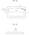
- FIG. 4A shows a planar structure of an organic electroluminescent display device according to a second embodiment of the present invention
- FIG. 4B is a perspective view showing steps for forming the lower electrode of FIG. 4A ;
- FIG. 4C is a plan view of the lower electrode of FIG. 4A ;
- FIG. 4D is a cross-sectional view taken along the line VII-VII of FIG. 4C .
- FIG. 3A shows a planar structure of an active matrix organic electroluminescent display device (AMOLED) according to a first embodiment of the present invention.
- the AMOLED of FIG. 3A illustrates a device consisting of two transistors and a capacitor.
- FIG. 3B shows a cross-sectional view taken along the line IV-IV of FIG. 3A .
- a buffer layer 340 is formed on a transparent insulating substrate 300 , such as a glass substrate.
- the substrate includes a non-emission region 310 and an emission region 330 .
- an amorphous silicon layer is deposited on the buffer layer 340 to form a semiconductor layer 311 .
- the semiconductor layer 311 is formed by performing a crystallization process after patterning the amorphous silicon layer.
- a gate insulating layer 350 is formed on the entire surface of the substrate, and a metallic material for a gate electrode is deposited and patterned on the gate insulating layer 350 to form a gate 312 over the semiconductor layer 311 .
- a capacitor lower electrode 322 is simultaneously formed at this time. Now, upon the formation of the gate 312 and the capacitor lower electrode 322 , a gate line 302 of FIG. 3A is also formed.
- source/drain regions 313 and 314 are formed by ion implantation of, for example, P or N type impurities, into the semiconductor layer 311 .
- an interlayer insulating layer 360 is formed on the entire surface of the substrate, and the interlayer insulating layer 360 and the gate insulating layer 350 are etched to expose a portion of the source/drain regions 313 and 314 . Thereby, contact holes 361 and 362 for source/drain electrodes are formed.
- the source/drain electrodes 315 and 316 are formed to contact with the source/drain regions 313 and 314 through the contact holes 361 and 362 .
- a capacitor upper electrode 326 is formed which extends from any one electrode, for example, the source electrode 315 , of the source/drain electrodes 315 and 316 , and at the same time, a data line 304 and a power line 306 of FIG. 3A are also formed.
- a passivation layer 370 is formed on the interlayer insulating layer 360 .
- the passivation layer 370 is etched to expose a portion of the other electrode, for example, the drain electrode 316 , of the source/drain electrodes 315 and 316 , thus forming a contact hole 371 for a pixel electrode.
- a transparent conductive layer is deposited on the passivation layer 370 in an emission region 330 , and is patterned to form a lower electrode 331 contacting with the drain electrode 316 through the contact hole 371 for the pixel electrode.
- FIGS. 3C to 3E steps for forming the lower electrode 331 of FIG. 3A are illustrated through FIGS. 3C to 3E .
- FIG. 3C is a perspective view showing a whole shape of the lower electrode 331
- FIG. 3D is a plan view of the lower electrode 331
- FIG. 3E is a cross-sectional view taken along the line V-V of FIG. 3D .
- the upper surface 331 a of the lower electrode 331 has a rectangular shape, and a lower surface 331 b of the lower electrode 331 has rounded corners, so that the lower electrode 331 is tapered.
- e 31 is the radius of curvature of the upper surface 331 a
- e 32 is the radius of curvature of the lower surface 331 b
- the lower electrode 331 has the upper surface 331 a in which the center of the radius of curvature e 31 is at its corners so that the radius of curvature is zero.
- the center of the radius of curvature e 32 of the lower surface 331 b is located at a point on the same axis as an axis perpendicular to a plane on which the center of the radius of curvature of the upper surface 331 a is positioned so that the radius of curvature e 32 is larger than zero.
- upper surface 331 a has four angled corners and the lower surface 331 b has four rounded corners. Accordingly, since the four corners of the lower electrode 331 are not angled, an open edge defect due to cut-off of the organic emission layer 332 can be prevented even after the organic emission layer 332 is deposited.
- an organic emission layer 332 is formed on the passivation layer 370 including the lower electrode 331 .
- an upper electrode 333 made of a metallic material is formed thereon, thereby creating the active matrix organic electroluminescent display device.
- the lower electrode acts as an anode electrode and the upper electrode acts as a cathode electrode.
- FIG. 4A shows a planar structure of an active matrix organic electroluminescent display device (AMOLED) according to a second embodiment of the present invention.
- the AMOLED of FIG. 4A illustrates a device having two transistors and a capacitor.
- FIG. 4B A cross-sectional view taken along the line VI-VI of FIG. 4B illustrates structure similar to that shown in FIG. 3B . Additionally, a method of manufacturing the second embodiment of the present invention will be easily understood by a person skilled in the art with reference to the above description given with regard to the first embodiment. Thus, FIG. 4A need not be described in detail.
- FIG. 4B is a perspective view showing a whole shape of the lower electrode 431
- FIG. 4C is a plan view of the lower electrode 431
- FIG. 4D is a cross-sectional view taken along the line VII-VII of FIG. 4C .
- the lower electrode 431 Upon the formation of the lower electrode 431 , shown in FIG. 4C , four corners of an inner portion of an upper surface 431 a are rounded on a plane, four corners of an outer portion of a lower surface 431 b are rounded. As shown in FIG. 4D , the lower electrode is formed to be tapered so that the lower surface 431 b is formed wider than upper surface 431 a.
- e 41 is the radius of curvature of the upper surface 431 a of the lower electrode 431
- e 42 is the radius of curvature of the lower surface 431 b of the lower electrode 431 .
- the lower electrode 431 has the upper surface 431 a whose four corners each have curvature and the center of the curvature is positioned on the upper surface 431 a .
- the center of the radius of curvature e 42 of the lower surface 431 b is at a point on the same axis as an axis perpendicular to a plane including the center of the radius of curvature e 41 of the upper surface 431 a , wherein the radius of curvature e 42 of the lower surface 431 b is larger than that of the upper surface 431 a , and the four corners of the lower surface 431 b are also rounded.
- the upper electrode (see 333 of FIG. 3B ) is formed on the organic emission layer ( 332 of FIG. 3B ) to supply a common power source.
- the lower electrode 431 is an anode electrode and the upper electrode formed on the organic emission layer is a cathode electrode.
- curvature of the lower electrode may also be provided at a side portion so that a shape of the surface of the lower electrode forms an oval or circular shape.
- the lower electrode in manufacturing an AMOLED having no pixel definition layer, is formed of a transparent metallic material and has the corners of its upper and lower surfaces rounded off, to prevent outgassing and short-induced defects.
- Such a configuration improves luminosity and increases the life of the organic electroluminescent display device.
Landscapes
- Physics & Mathematics (AREA)
- Optics & Photonics (AREA)
- Electroluminescent Light Sources (AREA)
- Devices For Indicating Variable Information By Combining Individual Elements (AREA)
Abstract
Description
e31=0,e32 32>0
e42>0,e41>0
Claims (10)
Applications Claiming Priority (2)
| Application Number | Priority Date | Filing Date | Title |
|---|---|---|---|
| KR2003-86154 | 2003-11-29 | ||
| KR1020030086154A KR100686341B1 (en) | 2003-11-29 | 2003-11-29 | Organic light emitting display device and manufacturing method thereof |
Publications (2)
| Publication Number | Publication Date |
|---|---|
| US20050116623A1 US20050116623A1 (en) | 2005-06-02 |
| US7294962B2 true US7294962B2 (en) | 2007-11-13 |
Family
ID=34464782
Family Applications (1)
| Application Number | Title | Priority Date | Filing Date |
|---|---|---|---|
| US10/937,294 Expired - Lifetime US7294962B2 (en) | 2003-11-29 | 2004-09-10 | Organic electroluminescent display device and method for manufacturing the same |
Country Status (5)
| Country | Link |
|---|---|
| US (1) | US7294962B2 (en) |
| EP (1) | EP1536473B1 (en) |
| JP (1) | JP2005327694A (en) |
| KR (1) | KR100686341B1 (en) |
| CN (1) | CN100440574C (en) |
Cited By (5)
| Publication number | Priority date | Publication date | Assignee | Title |
|---|---|---|---|---|
| US20110186846A1 (en) * | 2010-02-03 | 2011-08-04 | Samsung Mobile Display Co., Ltd. | Organic Light Emitting Display Device |
| US20110205198A1 (en) * | 2010-02-24 | 2011-08-25 | Samsung Mobile Display Co., Ltd. | Organic Light Emitting Display Device |
| US20130134452A1 (en) * | 2011-11-30 | 2013-05-30 | Canon Kabushiki Kaisha | Display device |
| US9343514B2 (en) | 2013-04-26 | 2016-05-17 | Samsung Display Co., Ltd. | Organic light emitting diode display and method of manufacturing the same |
| US12490598B2 (en) | 2019-12-31 | 2025-12-02 | Lg Display Co., Ltd. | Display device and method of manufacturing same |
Families Citing this family (11)
| Publication number | Priority date | Publication date | Assignee | Title |
|---|---|---|---|---|
| JP2006120622A (en) * | 2004-09-21 | 2006-05-11 | Canon Inc | Luminescent screen structure and image forming apparatus |
| EP1949455A1 (en) * | 2005-11-18 | 2008-07-30 | Semiconductor Energy Laboratory Co., Ltd. | Photoelectric conversion device |
| WO2009154168A1 (en) * | 2008-06-17 | 2009-12-23 | 株式会社日立製作所 | Organic light-emitting element, method for manufacturing the organic light-emitting element, apparatus for manufacturing the organic light-emitting element, and organic light-emitting device using the organic light-emitting element |
| GB201500748D0 (en) | 2015-01-16 | 2015-03-04 | Cambridge Display Tech Ltd | Method of forming a light-emitting device |
| KR102368849B1 (en) * | 2015-07-30 | 2022-02-28 | 엘지디스플레이 주식회사 | Organic light emitting display device |
| US10593657B2 (en) * | 2016-11-01 | 2020-03-17 | Innolux Corporation | Display devices and methods for forming the same |
| CN108054184B (en) * | 2017-12-11 | 2020-12-25 | 京东方科技集团股份有限公司 | Array substrate, preparation method and display device |
| CN109243305B (en) * | 2018-09-17 | 2021-10-12 | 京东方科技集团股份有限公司 | Display panel, display device, and method for manufacturing display panel |
| WO2021226744A1 (en) | 2020-05-09 | 2021-11-18 | 京东方科技集团股份有限公司 | Display panel and manufacturing method therefor, and display apparatus and manufacturing method therefor |
| US20240292697A1 (en) * | 2021-09-16 | 2024-08-29 | Semiconductor Energy Laboratory Co., Ltd. | Display device |
| US20240407211A1 (en) * | 2021-09-30 | 2024-12-05 | Semiconductor Energy Laboratory Co., Ltd. | Display device |
Citations (10)
| Publication number | Priority date | Publication date | Assignee | Title |
|---|---|---|---|---|
| JPH03105893A (en) | 1989-09-19 | 1991-05-02 | Fuji Electric Co Ltd | Manufacture of thin film electroluminescent device |
| JPH10255975A (en) | 1997-03-07 | 1998-09-25 | Seiko Epson Corp | Luminous display |
| EP0907304A1 (en) | 1996-05-29 | 1999-04-07 | Idemitsu Kosan Company Limited | Organic el device |
| JP2001110575A (en) | 1999-10-04 | 2001-04-20 | Sanyo Electric Co Ltd | Electroluminescence display device |
| JP2003022035A (en) | 2001-07-10 | 2003-01-24 | Sharp Corp | Organic EL panel and manufacturing method thereof |
| JP2003076332A (en) | 2001-08-31 | 2003-03-14 | Sanyo Electric Co Ltd | Driving circuit of display panel |
| EP1333497A2 (en) | 2002-02-01 | 2003-08-06 | Seiko Epson Corporation | Circuit substrate, electro-optical device and electronic appliances |
| US20030203527A1 (en) | 1999-05-27 | 2003-10-30 | Lg Philips Lcd Co., Ltp | Electro-luminescent display and a method of manufacturing the same |
| JP2003332082A (en) | 2002-05-15 | 2003-11-21 | Victor Co Of Japan Ltd | Organic electroluminescent device |
| JP2004355918A (en) | 2003-05-28 | 2004-12-16 | Sony Corp | Laminated structure and manufacturing method thereof, display element, and display device |
-
2003
- 2003-11-29 KR KR1020030086154A patent/KR100686341B1/en not_active Expired - Fee Related
-
2004
- 2004-06-23 JP JP2004185199A patent/JP2005327694A/en active Pending
- 2004-09-10 US US10/937,294 patent/US7294962B2/en not_active Expired - Lifetime
- 2004-09-29 CN CNB2004100117914A patent/CN100440574C/en not_active Expired - Lifetime
- 2004-11-29 EP EP04090474A patent/EP1536473B1/en not_active Expired - Lifetime
Patent Citations (11)
| Publication number | Priority date | Publication date | Assignee | Title |
|---|---|---|---|---|
| JPH03105893A (en) | 1989-09-19 | 1991-05-02 | Fuji Electric Co Ltd | Manufacture of thin film electroluminescent device |
| EP0907304A1 (en) | 1996-05-29 | 1999-04-07 | Idemitsu Kosan Company Limited | Organic el device |
| JPH10255975A (en) | 1997-03-07 | 1998-09-25 | Seiko Epson Corp | Luminous display |
| US20030203527A1 (en) | 1999-05-27 | 2003-10-30 | Lg Philips Lcd Co., Ltp | Electro-luminescent display and a method of manufacturing the same |
| JP2001110575A (en) | 1999-10-04 | 2001-04-20 | Sanyo Electric Co Ltd | Electroluminescence display device |
| US6727871B1 (en) | 1999-10-04 | 2004-04-27 | Sanyo Electric Co., Ltd. | Electroluminescence display apparatus |
| JP2003022035A (en) | 2001-07-10 | 2003-01-24 | Sharp Corp | Organic EL panel and manufacturing method thereof |
| JP2003076332A (en) | 2001-08-31 | 2003-03-14 | Sanyo Electric Co Ltd | Driving circuit of display panel |
| EP1333497A2 (en) | 2002-02-01 | 2003-08-06 | Seiko Epson Corporation | Circuit substrate, electro-optical device and electronic appliances |
| JP2003332082A (en) | 2002-05-15 | 2003-11-21 | Victor Co Of Japan Ltd | Organic electroluminescent device |
| JP2004355918A (en) | 2003-05-28 | 2004-12-16 | Sony Corp | Laminated structure and manufacturing method thereof, display element, and display device |
Non-Patent Citations (1)
| Title |
|---|
| European Search Report dated Feb. 23, 2005. |
Cited By (8)
| Publication number | Priority date | Publication date | Assignee | Title |
|---|---|---|---|---|
| US20110186846A1 (en) * | 2010-02-03 | 2011-08-04 | Samsung Mobile Display Co., Ltd. | Organic Light Emitting Display Device |
| US8461592B2 (en) | 2010-02-03 | 2013-06-11 | Samsung Display Co., Ltd. | Organic light emitting display device |
| US20110205198A1 (en) * | 2010-02-24 | 2011-08-25 | Samsung Mobile Display Co., Ltd. | Organic Light Emitting Display Device |
| US8664848B2 (en) | 2010-02-24 | 2014-03-04 | Samsung Display Co., Ltd. | Organic light emitting display device |
| US20130134452A1 (en) * | 2011-11-30 | 2013-05-30 | Canon Kabushiki Kaisha | Display device |
| US9012927B2 (en) * | 2011-11-30 | 2015-04-21 | Canon Kabushiki Kaisha | Display device |
| US9343514B2 (en) | 2013-04-26 | 2016-05-17 | Samsung Display Co., Ltd. | Organic light emitting diode display and method of manufacturing the same |
| US12490598B2 (en) | 2019-12-31 | 2025-12-02 | Lg Display Co., Ltd. | Display device and method of manufacturing same |
Also Published As
| Publication number | Publication date |
|---|---|
| CN1622728A (en) | 2005-06-01 |
| JP2005327694A (en) | 2005-11-24 |
| EP1536473B1 (en) | 2012-06-06 |
| KR100686341B1 (en) | 2007-02-22 |
| EP1536473A1 (en) | 2005-06-01 |
| CN100440574C (en) | 2008-12-03 |
| US20050116623A1 (en) | 2005-06-02 |
| KR20050052290A (en) | 2005-06-02 |
Similar Documents
| Publication | Publication Date | Title |
|---|---|---|
| US7492096B2 (en) | Flat panel display device capable of reducing or preventing a voltage drop and method of fabricating the same | |
| US7294962B2 (en) | Organic electroluminescent display device and method for manufacturing the same | |
| JP2006140145A (en) | Organic electroluminescence display | |
| KR100765522B1 (en) | Electroluminescent element and manufacturing method | |
| JP2005157312A (en) | Active matrix organic light emitting display device and method for manufacturing the same | |
| CN1700828B (en) | Organic el display and fabricating method thereof | |
| US20130119362A1 (en) | Organic light emitting diode display | |
| US7576354B2 (en) | Organic light emitting diode display and method of fabricating the same | |
| CN101834200B (en) | Organic RL display and fabricating method thereof | |
| KR20050099027A (en) | Top emission oled using assistant electrode to prevent ir drop and fabricating the same | |
| KR100617193B1 (en) | Bidirectional organic EL display device and manufacturing method thereof | |
| KR100741966B1 (en) | Organic light emitting display device and manufacturing method thereof | |
| CN1292394C (en) | Electroluminescent display device and manufacturing method thereof | |
| US20240215385A1 (en) | Display Apparatus Having an Auxiliary Electrode | |
| KR20100065685A (en) | Dual panel type organic electro luminescent device and method of fabricating the same | |
| KR100617114B1 (en) | Dual type organic EL display panel and its manufacturing method | |
| KR100638085B1 (en) | Organic electroluminescent display | |
| KR100739579B1 (en) | OLED display and manufacturing method thereof | |
| KR100728790B1 (en) | OLED display and manufacturing method thereof | |
| KR20180133308A (en) | Pattern structure for display device and manufacturing method thereof |
Legal Events
| Date | Code | Title | Description |
|---|---|---|---|
| AS | Assignment |
Owner name: SAMSUNG SDI CO., LTD., KOREA, REPUBLIC OF Free format text: ASSIGNMENT OF ASSIGNORS INTEREST;ASSIGNORS:KIM, MU-HYUN;KIM, KYONG-DO;REEL/FRAME:015787/0805 Effective date: 20040811 |
|
| STCF | Information on status: patent grant |
Free format text: PATENTED CASE |
|
| FEPP | Fee payment procedure |
Free format text: PAYOR NUMBER ASSIGNED (ORIGINAL EVENT CODE: ASPN); ENTITY STATUS OF PATENT OWNER: LARGE ENTITY |
|
| AS | Assignment |
Owner name: SAMSUNG MOBILE DISPLAY CO., LTD., KOREA, REPUBLIC Free format text: ASSIGNMENT OF ASSIGNORS INTEREST;ASSIGNOR:SAMSUNG SDI CO., LTD.;REEL/FRAME:022024/0026 Effective date: 20081212 Owner name: SAMSUNG MOBILE DISPLAY CO., LTD.,KOREA, REPUBLIC O Free format text: ASSIGNMENT OF ASSIGNORS INTEREST;ASSIGNOR:SAMSUNG SDI CO., LTD.;REEL/FRAME:022024/0026 Effective date: 20081212 |
|
| FPAY | Fee payment |
Year of fee payment: 4 |
|
| AS | Assignment |
Owner name: SAMSUNG DISPLAY CO., LTD., KOREA, REPUBLIC OF Free format text: MERGER;ASSIGNOR:SAMSUNG MOBILE DISPLAY CO., LTD.;REEL/FRAME:028884/0453 Effective date: 20120702 |
|
| FEPP | Fee payment procedure |
Free format text: PAYOR NUMBER ASSIGNED (ORIGINAL EVENT CODE: ASPN); ENTITY STATUS OF PATENT OWNER: LARGE ENTITY Free format text: PAYER NUMBER DE-ASSIGNED (ORIGINAL EVENT CODE: RMPN); ENTITY STATUS OF PATENT OWNER: LARGE ENTITY |
|
| FPAY | Fee payment |
Year of fee payment: 8 |
|
| MAFP | Maintenance fee payment |
Free format text: PAYMENT OF MAINTENANCE FEE, 12TH YEAR, LARGE ENTITY (ORIGINAL EVENT CODE: M1553); ENTITY STATUS OF PATENT OWNER: LARGE ENTITY Year of fee payment: 12 |