JP2006120622A - Luminescent screen structure and image forming apparatus - Google Patents
Luminescent screen structure and image forming apparatus Download PDFInfo
- Publication number
- JP2006120622A JP2006120622A JP2005258742A JP2005258742A JP2006120622A JP 2006120622 A JP2006120622 A JP 2006120622A JP 2005258742 A JP2005258742 A JP 2005258742A JP 2005258742 A JP2005258742 A JP 2005258742A JP 2006120622 A JP2006120622 A JP 2006120622A
- Authority
- JP
- Japan
- Prior art keywords
- strip
- electron
- metal back
- light emitting
- screen structure
- Prior art date
- Legal status (The legal status is an assumption and is not a legal conclusion. Google has not performed a legal analysis and makes no representation as to the accuracy of the status listed.)
- Pending
Links
- 239000002184 metal Substances 0.000 claims abstract description 84
- 239000000463 material Substances 0.000 claims abstract description 16
- 239000000758 substrate Substances 0.000 claims description 54
- 230000015572 biosynthetic process Effects 0.000 claims description 2
- 239000011159 matrix material Substances 0.000 abstract description 35
- OAICVXFJPJFONN-UHFFFAOYSA-N Phosphorus Chemical compound [P] OAICVXFJPJFONN-UHFFFAOYSA-N 0.000 abstract description 27
- 239000010408 film Substances 0.000 description 22
- 238000010894 electron beam technology Methods 0.000 description 16
- 238000010586 diagram Methods 0.000 description 14
- 238000000034 method Methods 0.000 description 10
- 230000015556 catabolic process Effects 0.000 description 6
- 230000006378 damage Effects 0.000 description 6
- 239000011521 glass Substances 0.000 description 5
- 230000007547 defect Effects 0.000 description 4
- 230000002542 deteriorative effect Effects 0.000 description 4
- 238000004519 manufacturing process Methods 0.000 description 4
- 238000007740 vapor deposition Methods 0.000 description 4
- 230000005684 electric field Effects 0.000 description 3
- 239000010409 thin film Substances 0.000 description 3
- 230000001133 acceleration Effects 0.000 description 2
- 239000003990 capacitor Substances 0.000 description 2
- 238000007639 printing Methods 0.000 description 2
- OKTJSMMVPCPJKN-UHFFFAOYSA-N Carbon Chemical compound [C] OKTJSMMVPCPJKN-UHFFFAOYSA-N 0.000 description 1
- 206010034972 Photosensitivity reaction Diseases 0.000 description 1
- NIXOWILDQLNWCW-UHFFFAOYSA-N acrylic acid group Chemical group C(C=C)(=O)O NIXOWILDQLNWCW-UHFFFAOYSA-N 0.000 description 1
- 230000002411 adverse Effects 0.000 description 1
- 239000011230 binding agent Substances 0.000 description 1
- 239000012141 concentrate Substances 0.000 description 1
- 239000000470 constituent Substances 0.000 description 1
- 238000000151 deposition Methods 0.000 description 1
- 230000008021 deposition Effects 0.000 description 1
- 238000007599 discharging Methods 0.000 description 1
- 230000000694 effects Effects 0.000 description 1
- 239000000839 emulsion Substances 0.000 description 1
- 238000010304 firing Methods 0.000 description 1
- 229910002804 graphite Inorganic materials 0.000 description 1
- 239000010439 graphite Substances 0.000 description 1
- 230000003760 hair shine Effects 0.000 description 1
- 239000011810 insulating material Substances 0.000 description 1
- 150000002500 ions Chemical class 0.000 description 1
- 239000004973 liquid crystal related substance Substances 0.000 description 1
- 238000001259 photo etching Methods 0.000 description 1
- 238000000206 photolithography Methods 0.000 description 1
- 230000036211 photosensitivity Effects 0.000 description 1
- 238000001556 precipitation Methods 0.000 description 1
- 238000007650 screen-printing Methods 0.000 description 1
- 238000007789 sealing Methods 0.000 description 1
- 239000007921 spray Substances 0.000 description 1
- 238000004544 sputter deposition Methods 0.000 description 1
- 239000000126 substance Substances 0.000 description 1
- 238000001771 vacuum deposition Methods 0.000 description 1
Images


Classifications
-
- H—ELECTRICITY
- H01—ELECTRIC ELEMENTS
- H01J—ELECTRIC DISCHARGE TUBES OR DISCHARGE LAMPS
- H01J29/00—Details of cathode-ray tubes or of electron-beam tubes of the types covered by group H01J31/00
- H01J29/02—Electrodes; Screens; Mounting, supporting, spacing or insulating thereof
- H01J29/08—Electrodes intimately associated with a screen on or from which an image or pattern is formed, picked-up, converted or stored, e.g. backing-plates for storage tubes or collecting secondary electrons
- H01J29/085—Anode plates, e.g. for screens of flat panel displays
-
- H—ELECTRICITY
- H01—ELECTRIC ELEMENTS
- H01J—ELECTRIC DISCHARGE TUBES OR DISCHARGE LAMPS
- H01J1/00—Details of electrodes, of magnetic control means, of screens, or of the mounting or spacing thereof, common to two or more basic types of discharge tubes or lamps
- H01J1/02—Main electrodes
- H01J1/30—Cold cathodes, e.g. field-emissive cathode
-
- H—ELECTRICITY
- H01—ELECTRIC ELEMENTS
- H01J—ELECTRIC DISCHARGE TUBES OR DISCHARGE LAMPS
- H01J29/00—Details of cathode-ray tubes or of electron-beam tubes of the types covered by group H01J31/00
- H01J29/02—Electrodes; Screens; Mounting, supporting, spacing or insulating thereof
- H01J29/10—Screens on or from which an image or pattern is formed, picked up, converted or stored
- H01J29/18—Luminescent screens
- H01J29/28—Luminescent screens with protective, conductive or reflective layers
-
- H—ELECTRICITY
- H01—ELECTRIC ELEMENTS
- H01J—ELECTRIC DISCHARGE TUBES OR DISCHARGE LAMPS
- H01J31/00—Cathode ray tubes; Electron beam tubes
- H01J31/08—Cathode ray tubes; Electron beam tubes having a screen on or from which an image or pattern is formed, picked up, converted, or stored
- H01J31/10—Image or pattern display tubes, i.e. having electrical input and optical output; Flying-spot tubes for scanning purposes
- H01J31/12—Image or pattern display tubes, i.e. having electrical input and optical output; Flying-spot tubes for scanning purposes with luminescent screen
- H01J31/123—Flat display tubes
- H01J31/125—Flat display tubes provided with control means permitting the electron beam to reach selected parts of the screen, e.g. digital selection
- H01J31/127—Flat display tubes provided with control means permitting the electron beam to reach selected parts of the screen, e.g. digital selection using large area or array sources, i.e. essentially a source for each pixel group
-
- H—ELECTRICITY
- H01—ELECTRIC ELEMENTS
- H01J—ELECTRIC DISCHARGE TUBES OR DISCHARGE LAMPS
- H01J2329/00—Electron emission display panels, e.g. field emission display panels
- H01J2329/02—Electrodes other than control electrodes
- H01J2329/08—Anode electrodes
-
- H—ELECTRICITY
- H01—ELECTRIC ELEMENTS
- H01J—ELECTRIC DISCHARGE TUBES OR DISCHARGE LAMPS
- H01J2329/00—Electron emission display panels, e.g. field emission display panels
- H01J2329/18—Luminescent screens
- H01J2329/28—Luminescent screens with protective, conductive or reflective layers
Abstract
Description
本発明は、フィールドエミッションディスプレイ(FED)などの電子線を利用した平面型の画像形成装置において、電子線照射によって発光して画像を形成する発光スクリーン構造と、該発光スクリーン構造を用いた画像形成装置に関する。 The present invention relates to a planar image forming apparatus using an electron beam such as a field emission display (FED), a light emitting screen structure that emits light by electron beam irradiation to form an image, and an image formation using the light emitting screen structure Relates to the device.
従来、電子放出素子の利用形態としては、画像形成装置が挙げられる。例えば、冷陰極電子放出素子を多数形成した電子源基板と、電子放出素子から放出された電子を加速するメタルバック或いは透明電極、及び蛍光体を具備した対向基板とを平行に対向させ、真空に排気した平面型の電子線表示パネルが知られている。平面型の電子線表示パネルは、現在広く用いられている陰極線管(CRT)表示装置に比べ、軽量化、大画面化を図ることができ、好ましい。また、液晶を利用した平面型表示パネルやプラズマ・ディスプレイ、エレクトロルミネッセント・ディスプレイ等の他の平面型表示パネルに比べて、より高輝度、高品質な画像を提供することができる。 2. Description of the Related Art Conventionally, an image forming apparatus is used as an application form of an electron-emitting device. For example, an electron source substrate on which a large number of cold cathode electron-emitting devices are formed and a counter substrate having a metal back or transparent electrode for accelerating electrons emitted from the electron-emitting devices and a phosphor and facing each other in parallel are evacuated. An exhausted flat type electron beam display panel is known. A flat-type electron beam display panel is preferable because it can achieve lighter weight and larger screen than a cathode ray tube (CRT) display device that is widely used at present. In addition, it is possible to provide an image with higher brightness and higher quality than other flat display panels such as a flat display panel using liquid crystal, a plasma display, and an electroluminescent display.
このように、冷陰極電子放出素子から放出された電子を加速するために、メタルバックや透明電極等の対向電極と電子放出素子との間に電圧を印加するタイプの画像形成装置においては、発光輝度を最大限得るために高電圧を印加するのが有利である。電子放出素子の種類によって放出される電子線は対向電極に到達するまでに発散するので、高解像度のディスプレーを実現しようとすると、電子源基板と対向基板との基板間距離が短いのが好ましい。 Thus, in an image forming apparatus of a type in which a voltage is applied between a counter electrode such as a metal back or a transparent electrode and an electron-emitting device in order to accelerate electrons emitted from the cold cathode electron-emitting device, light emission It is advantageous to apply a high voltage in order to obtain the maximum brightness. Since the electron beam emitted by the type of the electron-emitting device diverges before reaching the counter electrode, it is preferable that the distance between the electron source substrate and the counter substrate is short in order to realize a high-resolution display.
しかしながら、基板間距離が短くなると必然的に該基板間が高電界となるため、不慮の放電により電子放出素子が破壊される現象が、まれに発生する場合がある。この場合、蛍光体の一部に集中して電流が流れるため、表示画面の一部が光る現象などが生じる。 However, when the distance between the substrates is shortened, a high electric field is inevitably generated between the substrates, so that a phenomenon that the electron-emitting device is destroyed due to accidental discharge may occur in rare cases. In this case, since a current flows concentrated on a part of the phosphor, a phenomenon that a part of the display screen shines occurs.
このような問題の解決のためには不慮の放電の頻度を減らすか、放電破壊を生じにくくする必要がある。 In order to solve such a problem, it is necessary to reduce the frequency of accidental discharge or to make it difficult to cause discharge breakdown.
電子放出素子の放電破壊の原因としては、短時間に1点に集中して大電流が流入して生じる発熱や、電子放出素子にかかる電圧が瞬時に上昇し、過電圧が印加されることによると考えられる。 The cause of the discharge breakdown of the electron-emitting device is that heat is generated when a large current flows in a single point in a short time, or the voltage applied to the electron-emitting device rises instantaneously and an overvoltage is applied. Conceivable.
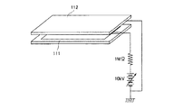
放電破壊の原因となる電流を減らす手段としては、図11に示すように制限抵抗を直列に挿入する方法が考えられる(図中の111は陽極であるフェースプレート、112は電子放出素子を備えたリアプレート)。しかし、例えば、縦500素子×横1000素子がマトリクス配線され、線順次で駆動されると、同時におよそ1000程度の素子がON状態となるため、本デバイスにこの方法を採用すると次のような問題が生じる。 As a means for reducing the current causing the discharge breakdown, a method of inserting a limiting resistor in series as shown in FIG. 11 is conceivable (in the figure, 111 is a face plate which is an anode, and 112 is provided with an electron-emitting device). Rear plate). However, for example, when 500 vertical elements × 1000 horizontal elements are arranged in a matrix and are driven in line sequence, about 1000 elements are simultaneously turned on. Occurs.
10kVの高電圧を陽極に印加した状態で、1000程度の素子がON状態となる場合に、1素子あたりの放出電流を5μAと仮定すると、画像パターン(点灯パターン)によって、0〜5mAの範囲で、陽極への流入電流が変動することになる。図11のように、1MΩの直列抵抗を陽極に接続する例では、直列抵抗部分での電圧降下が0〜5kVとなり、最大50%程度の輝度ムラを生じてしまう。 When a high voltage of 10 kV is applied to the anode and about 1000 elements are turned on, assuming that the emission current per element is 5 μA, the range of 0 to 5 mA depending on the image pattern (lighting pattern). The current flowing into the anode will fluctuate. As shown in FIG. 11, in the example in which a series resistance of 1 MΩ is connected to the anode, the voltage drop in the series resistance portion is 0 to 5 kV, and the luminance unevenness is about 50% at the maximum.
また、対向する平板に高電圧が印加されているので、コンデンサーとして蓄積される電荷は、例えば図11のフェースプレート111、リアプレート112の面積が100cm2、その間隔が1mm、両基板間の電位差が10kVとすると10-6クーロンに達する。これは、1μsecで放電しても1箇所に1Aの電流が集中する事になる。この放電電流が原因で素子破壊をもたらすので、前述の輝度むら問題が無いとしても、外部直列抵抗付加では問題の充分な解決とはならない。
Further, since a high voltage is applied to the opposing flat plates, the charge accumulated as a capacitor is, for example, the area of the
これらの課題に対し本出願人は、電圧を印加する電極を走査配線の方向と非平行に分割し、電極と加速電圧印加手段との間に抵抗体を設けることにより、対向する平板で発生する放電電流の抑制を行うことを提案した(特許文献1参照)。図12はその1例を示したものであり、図13はその等価回路を示したものである。図中、121は分割された電極(例えばITO膜)であり、片側を抵抗体122(例えばNiO膜)を介し、共通電極125で束ねてある。そして高電圧を端子123から印加できるようにしている。また、131はフェースプレート、132はリアプレートである。
In response to these problems, the present applicant divides an electrode to which a voltage is applied in a direction non-parallel to the direction of the scanning wiring, and generates a resistor between the electrode and the acceleration voltage applying means, thereby generating on an opposing flat plate. It has been proposed to suppress the discharge current (see Patent Document 1). FIG. 12 shows an example thereof, and FIG. 13 shows an equivalent circuit thereof. In the figure,
図13のようにフェースプレート131の電極を分割し、それぞれに高抵抗R1を挿入することでコンデンサー容量を低減させ、放電電流Ib2を低減している。これによって放電電流Ib2による、素子への印加電圧の変動も軽減され、放電時のダメージも改善される。
As shown in FIG. 13, the electrodes of the
しかしながら、放電時に電子放出素子にダメージを与えないと言う観点からは、さらに放電電流を低減するための構成が望まれていた。 However, from the viewpoint of not damaging the electron-emitting device during discharge, a configuration for further reducing the discharge current has been desired.
本発明は、輝度低下を伴わず、放電電流をさらに低減するための発光スクリーン構造を提供するものである。また、該発光スクリーン構造を用いた画像形成装置においては、不慮の放電による電子放出素子への悪影響を緩和し、良好な耐久性、長寿命化を実現することを目的とする。 The present invention provides a light emitting screen structure for further reducing the discharge current without lowering the luminance. Another object of the image forming apparatus using the light emitting screen structure is to alleviate the adverse effect on the electron-emitting device due to accidental discharge, and to achieve good durability and long life.
本発明の第一は、基板と、
前記基板上に位置する複数の発光部材と、
第一の方向及び該第一の方向と非平行な第二の方向に分割され、各々が少なくとも一つの前記発光部材を覆う複数のメタルバックと、
前記複数のメタルバックの内の少なくとも一部を電気的に接続し、前記第一の方向に延びる複数の短冊状抵抗体と
を有する発光スクリーン構造であって、
前記短冊状抵抗体は、前記第二の方向におけるメタルバックの間隙部において不連続であることを特徴とする。
The first of the present invention is a substrate,
A plurality of light emitting members located on the substrate;
A plurality of metal backs divided in a first direction and a second direction non-parallel to the first direction, each covering at least one light emitting member;
A light emitting screen structure having a plurality of strip-shaped resistors that electrically connect at least a part of the plurality of metal backs and extend in the first direction,
The strip-shaped resistor is discontinuous in the gap portion of the metal back in the second direction.
本発明の第二は、複数の電子放出素子と、前記第一の方向に平行であって、前記複数の電子放出素子のうちの少なくとも一部の電子放出素子を電気的に接続する複数の信号配線と、前記第二の方向に平行であって、前記複数の電子放出素子のうちの少なくとも一部の電子放出素子を電気的に接続する複数の走査配線とを備えた電子源と、前記電子放出素子から放出された電子の照射によって発光する発光スクリーン構造とを備えた画像形成装置であって、前記発光スクリーン構造が、上記本発明第一の発光スクリーン構造であることを特徴とする。 According to a second aspect of the present invention, there are provided a plurality of electron-emitting devices and a plurality of signals that are parallel to the first direction and electrically connect at least some of the plurality of electron-emitting devices. An electron source comprising a wiring and a plurality of scanning wirings parallel to the second direction and electrically connecting at least some of the plurality of electron-emitting devices; An image forming apparatus including a light emitting screen structure that emits light by irradiation of electrons emitted from an emitting element, wherein the light emitting screen structure is the first light emitting screen structure of the present invention.
本発明では、走査配線と非平行に分割されている短冊状抵抗体を用いるため、駆動時の電圧降下が低減され、さらにX方向(第二の方向であり、好ましくは走査配線方向)において、該短冊状抵抗体が隣接するメタルバック電極の間隙において不連続である。これによって、メタルバック電極間の抵抗が大きく、発光体基板(発光スクリーン構造)と電子源基板と間で不慮の放電が生じた際にも、該放電による電子放出素子のダメージが小さい。よって、本発明によれば、放電による電子放出素子のダメージが緩和され、良好な耐久性、長寿命化を図った信頼性の高い画像形成装置が提供される。 In the present invention, since a strip-shaped resistor that is divided non-parallel to the scanning wiring is used, the voltage drop during driving is reduced, and in the X direction (second direction, preferably the scanning wiring direction), The strip-shaped resistor is discontinuous in the gap between adjacent metal back electrodes. As a result, the resistance between the metal back electrodes is large, and even when an unexpected discharge occurs between the light emitter substrate (light emitting screen structure) and the electron source substrate, damage to the electron-emitting device due to the discharge is small. Therefore, according to the present invention, it is possible to provide a highly reliable image forming apparatus in which damage to the electron-emitting device due to discharge is mitigated and good durability and long life are achieved.
本発明の発光体基板においては、X方向において複数に分割された短冊状抵抗体が、X方向において少なくとも2以上に分割されたメタルバック電極の電極間隙において不連続になるように、好ましくはメタルバック電極内側に配置されている。この構成により、X方向において隣接するメタルバック電極間の抵抗が高抵抗に保持され、X方向におけるメタルバック電極間の放電電流の流れ込みが防止される。まずはじめに、当該作用について、X方向において短冊状抵抗体が、隣接するメタルバック電極の間隙において連続する構成と比較して説明する。 In the light emitter substrate of the present invention, the strip-shaped resistor divided into a plurality in the X direction is preferably a metal so that it is discontinuous in the electrode gap of the metal back electrode divided into at least two in the X direction. Arranged inside the back electrode. With this configuration, the resistance between the metal back electrodes adjacent in the X direction is maintained at a high resistance, and the discharge current between the metal back electrodes in the X direction is prevented from flowing. First, the operation will be described in comparison with a configuration in which strip resistors are continuous in the gap between adjacent metal back electrodes in the X direction.
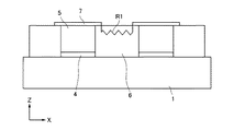
図14は、本発明の発光体基板の好ましい実施形態における、基板に直交する方向の部分断面図(後述する図1(a)のA−A’断面図に相当する)である。図中、1は基板、4は短冊状抵抗体、5は蛍光体(発光部材)、6はブラックマトリクス(黒色部材)、7はメタルバック電極であり、短冊状抵抗体4がメタルバック電極7内に配置している。また、図15は、短冊状抵抗体4がX方向においてメタルバック電極7間隙において連続する(短冊状抵抗体4がメタルバック電極7間隙を跨ぐ)構成の部分断面図である。
FIG. 14 is a partial cross-sectional view (corresponding to a cross-sectional view taken along the line A-A ′ of FIG. 1A described later) in a direction perpendicular to the substrate in the preferred embodiment of the light emitter substrate of the present invention. In the figure, 1 is a substrate, 4 is a strip resistor, 5 is a phosphor (light emitting member), 6 is a black matrix (black member), 7 is a metal back electrode, and the
図14,図15の構成において、ブラックマトリクス6の膜厚方向(Z方向)の抵抗値をR2、膜面方向(X方向)の抵抗値をR1とし、短冊状抵抗体4の抵抗は無視できるとすると、図14の構成では、X方向におけるメタルバック電極7間の抵抗RはR1である。一方、図15の構成では、隣接するメタルバック電極7間の電流経路として、膜面方向に進む経路と、ブラックマトリクス6を膜厚方向に移動して短冊状抵抗体4を経由する経路とが存在する。このため、隣接するメタルバック電極7間の合成抵抗値R’は、R’=1/{(1/R1)+(1/2R2)}=(R1・2R2)/(2R2+R1)である。一方、図14のRと比較すると、R=R1=R1(2R2+R1)/(2R2+R1)={(2R1・R2)+(R1)2}/(2R2+R1)=R’+{(R1)2/(2R2+R1)}となる。つまり、本発明である図14の構成は、図15の構成に比較して、メタルバック電極7間の抵抗値が(R1)2/(2R2+R1)分だけ高抵抗化し、よって放電電流の流れ込みを低減できるのである。
14 and 15, the resistance value in the film thickness direction (Z direction) of the
尚、上記説明においては、本発明の発光体基板として好ましい、短冊状抵抗体4がメタルバック電極7の内側に配置した構成を示した。しかし、本発明においては、図15に示したような、ブラックマトリクス6内の膜厚方向と短冊状抵抗体4を介した電流経路が、形成されない範囲であれば、短冊状抵抗体4がメタルバック電極7間隙に配置していても構わない。具体的には、ブラックマトリクスの膜厚方向と短冊状抵抗体4を経由する抵抗が、ブラックマトリクス6の膜面方向の抵抗よりも大きくなるように、短冊状抵抗体4を不連続にすればよい。
In the above description, a configuration in which the strip-
また、Y方向(第一の方向)においては、隣接するメタルバック電極7間の距離がX方向(第二の方向)よりも大きいため、短冊状抵抗体4がメタルバック電極7間に配置されていても抵抗を大きくすることができ、放電電流に与える影響は小さい。
Further, in the Y direction (first direction), the distance between the adjacent metal back
以下、本発明の発光体基板(フェースプレートと記述する場合もある)の基本構成について、図1を用いて説明する。 Hereinafter, a basic configuration of a light emitter substrate (sometimes referred to as a face plate) of the present invention will be described with reference to FIG.
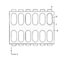
図1は本発明の発光体基板の好ましい一実施形態の構成を示す模式図であり、図1(a)は平面図、(b)は(a)のA−A’断面図であり、(a)は各々の位置関係を分かりやすくするために、部材の一部を切り欠いて示している。図1において、1はガラス等透明絶縁材からなる基板、2は共通電極、3は直列抵抗体、4はX方向において複数に分割された短冊状抵抗体である。5は蛍光体(発光部材)であり、短冊状抵抗体4は該蛍光体5の下部に配置されている。さらに短冊状抵抗体4は直列抵抗体3を介して共通電極2に接続されており、高圧印加端子(不図示)を介して高電圧が印加される。6は隣接する蛍光体5間を遮光するブラックマトリクス(黒色部材)である。7はメタルバック電極(以下、メタルバックと記す)であり、本実施形態では蛍光体5に対応して(即ち画素毎に)、X及びY方向において分割されており、蛍光体5の前面(後述するリアプレート側)に位置するように配置されている。
FIG. 1 is a schematic view showing a configuration of a preferred embodiment of a light emitter substrate of the present invention, FIG. 1 (a) is a plan view, FIG. 1 (b) is a cross-sectional view along AA ′ of FIG. In FIG. 5A, a part of the member is notched for easy understanding of the positional relationship. In FIG. 1, 1 is a substrate made of a transparent insulating material such as glass, 2 is a common electrode, 3 is a series resistor, and 4 is a strip-shaped resistor divided into a plurality in the X direction.
本発明において、短冊状抵抗体4は、X方向において隣接するメタルバック間に渡って位置しないようにするため、メタルバック7のY方向に平行なエッジよりも内側に配置されていることが好ましく、蛍光体5の下部に配置するのが好ましい。また、短冊状抵抗体4は抵抗を制御できるものであれば良く、蛍光体5の下部に配置する場合は透明電極を用いることができる。その場合ITO等を用いることができる。
In the present invention, the strip-shaped
また、メタルバック7は、X方向において少なくとも2以上に分割され、各メタルバック7はブラックマトリクス6により短冊状抵抗体4と電気的に接続されている。
The metal back 7 is divided into at least two or more in the X direction, and each metal back 7 is electrically connected to the strip-shaped
図1の様に1蛍光体単位でメタルバック7を分割した方が許容される電圧降下の範囲内で短冊状抵抗体4の抵抗を高くできるので、より放電電流を低減することができ、好ましい。しかし、メタルバックの大きさはこれに限られるものではなく、例えば、図5や図7で示されるような3蛍光体単位(例えば、R,G,B)や図8で示されるような6画素単位と適宜選択することができる。
As shown in FIG. 1, it is preferable to divide the metal back 7 in units of one phosphor, because the resistance of the strip-shaped
X方向に平行な走査配線に非平行に、即ち図1の実施形態においてはY方向に平行に配置される短冊状抵抗体4は、画像形成装置の駆動時に電圧降下による輝度低下が著しく発生しない程度の抵抗値であればよい。具体的には、1電子放出素子の放出電流が1〜10μAの場合、短冊状抵抗体の抵抗は、1kΩ〜1GΩが好ましい。短冊状抵抗体の抵抗値の実用的な上限は、電圧降下が印加電圧の1〜数割程度以下で輝度ムラを生じない範囲で決められる。
The strip-
短冊状抵抗体4と共通電極2とをつなぐ直列抵抗体3の抵抗値は、共通電極2近傍で放電が発生した場合においても、リアプレートに流れる放電電流を制限しなければならない。よって、具体的には、10kΩ〜1GΩの間が好ましく、さらに10kΩ〜10MGの間であると好適である。
The resistance value of the
本実施形態において、ブラックマトリクス6は、短冊状抵抗体4とメタルバック7を電気的に接続している。放電電流を制限する目的から、ブラックマトリクスの抵抗は、各々のメタルバック7間において1kΩ〜1GΩとするのが好ましく、1kΩ〜1MΩの間であるとより好適である。ブラックマトリクス6の材料としては、通常用いられている黒鉛を主成分とする材料の他、光の透過及び反射が少ない材料であれば、用いることができる。
In the present embodiment, the
図2に本発明の発光体基板を用いた画像形成装置の一例として、表面伝導型の電子放出素子を用いてなる表示パネルの概略構成図を示す。図2は一部を切り欠いた状態の表示パネルを示している。図中、11は電子源基板、17は陽極(アノード)基板であるフェースプレート、16は外枠、15はリアプレートであり、これらにより真空外囲器18を構成している。14は電子放出素子である。12は走査配線(走査電極)、13は信号配線(信号電極)であり、それぞれ、電子放出素子14の素子電極に接続されている。フェースプレート17の構成部材については、図1と同じ符号を付した。
FIG. 2 shows a schematic configuration diagram of a display panel using a surface conduction electron-emitting device as an example of an image forming apparatus using the light emitter substrate of the present invention. FIG. 2 shows the display panel with a part cut away. In the figure, 11 is an electron source substrate, 17 is a face plate which is an anode (anode) substrate, 16 is an outer frame, and 15 is a rear plate, and these constitute a
この表示パネルにおいて画像を形成するには、マトリクス状に配置された走査配線12と信号配線13に所定の電圧を順次印加することで、マトリクスの交点に位置する所定の電子放出素子14を選択的に駆動する。これによって放出された電子を蛍光体5に照射させ、所定の位置に輝点を得る。尚、メタルバック7は、放出電子を加速してより高い輝度の輝点を得るために、電子放出素子14に対して高電位となるように高電圧Hvが印加される。ここで、印加される電圧は、蛍光体5の性能にもよるが、数百V〜数十kV程度の電圧である。従って、リアプレート11とフェースプレート17間の距離は、この印加電圧によって真空の絶縁破壊(即ち放電)が生じないようにするため、百μm〜数mm程度に設定されるのが一般的である。
In order to form an image on this display panel, a predetermined voltage is sequentially applied to the
カラーの蛍光膜の場合は、R(赤)、G(緑)、B(青)の各色の蛍光体5を用い、基板1に蛍光体5を塗布する方法としては、モノクローム、カラーによらず、沈殿法、印刷法等が採用できる。
In the case of a color fluorescent film, the
メタルバック7を用いる目的は、蛍光体5の発光のうち内面側への光を基板1側へ鏡面反射させることにより輝度を向上させることである。また電子ビームの加速電圧を印加するための電極として作用させること、真空外囲器18内で発生した負イオンの衝突によるダメージから蛍光体5を保護すること等である。
The purpose of using the metal back 7 is to improve the luminance by specularly reflecting the light emitted from the
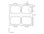
尚、メタルバック7の形状は方形の角部に曲率を持たせた形状にすることが好ましい。フェースプレート17とリアプレート11間で放電が生じた場合に、隣接するメタルバック7間に電位差が生じるため、角部に曲率を持たないと電界が集中し、沿面放電を生じる場合があるためである。角部に曲率を有するメタルバックの一例を図3,図6に示す。図中、31は電子ビーム形状である。このような角部が曲率を有する場合、曲率としてはなるべく大きいほうが放電のしにくさを考えると好ましいが、電子ビームの照射エリア、形状を鑑み、設定する必要がある。本発明に用いられる表面伝導型電子放出素子(SEC)では照射される電子ビーム形状31は円弧形状のため、ビームの2次元形状に対応した曲率に近くすることがさらに好ましい。
In addition, it is preferable that the shape of the metal back 7 is a shape in which a corner of the square has a curvature. When a discharge is generated between the
このような分割されたメタルバック7を形成するには、通常の方法で蛍光体5が形成された基板全面にメタルバックを形成し、フォトエッチングによりパターニングする方法が利用できる。また、所望の開口を有するメタルマスクを遮蔽部材として用いて蒸着する(通常マスク蒸着と呼ぶ)方法等を適時選択することができる。
In order to form such a divided metal back 7, it is possible to use a method in which a metal back is formed on the entire surface of the substrate on which the
さらに、本発明の発光体基板を用いて画像形成装置を作製する場合に、真空外囲器18内を長期間に渡り高真空に維持するためにゲッター材を有していてもよい。その場合、電子放出素子14から放出された電子線が照射される電子線照射領域を避けて、ゲッター材を配置することが好ましい。電子照射領域にゲッタ材を配置すると、電子線のエネルギーを低下させ、所望の輝度が得られなくなってしまうからである。図9,図10にゲッター材を配置した構成例の模式図を示す。図中、93は電子放出素子14から放出された電子線、94は電子線93の照射範囲、95はゲッター材である。また、図9は部分断面図、図10はリアプレート側から見たフェースプレート17の平面図である。尚、ゲッター材の被覆面は、ゲッターの形成量を増加させるため粗面であることが望ましい。
Furthermore, when an image forming apparatus is manufactured using the light emitter substrate of the present invention, a getter material may be included in order to maintain a high vacuum in the
(実施例1)
図1に示す構成のフェースプレートを作製した。作製方法を説明する。
(Example 1)
A face plate having the structure shown in FIG. 1 was produced. A manufacturing method will be described.
基板1として厚さ2.8mmのガラス基板(PD200、旭硝子社製)を用い、全面に厚さ100nmのITO膜を形成した後、フォトリソグラフィー工程で幅185μmの短冊形状にパターニングし、短冊状抵抗体4を形成した。短冊状抵抗体4の抵抗が200MΩ程度になるようにITO膜のシート抵抗は60kΩ/□に調整した。
A glass substrate (PD200, manufactured by Asahi Glass Co., Ltd.) having a thickness of 2.8 mm is used as the
次に短冊状抵抗体4の両側に直列抵抗体3としてパターニングしたNiO膜を形成し、全ての抵抗体3と接するようにAgペーストを用いて共通電極2を形成した。直列抵抗体3の抵抗値は10MΩとした。
Next, a patterned NiO film was formed as a
上記短冊状抵抗体4上に、ブラックマトリクス6(NP−7803D、ノリタケ機材(株)製)を印刷し、隣接するメタルバック7間の抵抗(個別抵抗)が100kΩ程度になるようにした。さらに、蛍光体5を塗布焼成した。
A black matrix 6 (NP-7803D, manufactured by Noritake Equipment Co., Ltd.) was printed on the strip-shaped
最後に、蛍光体4の上に島状のAl膜を厚さ80nmに蒸着し、メタルバック7を形成した。このようにして、短冊状抵抗体4が、X方向において隣接するメタルバック間において連続しない構成のフェースプレートを作成した。
Finally, an island-shaped Al film was deposited on the
上述で作製したフェースプレート17を用い、図2に示した画像形成装置を作成した。具体的には、走査配線12、信号配線13、電子放出素子14を形成した電子源基板11をリアプレート15上に配置し、リアプレートと上述のフェースプレートとを外枠16を介在させて封着した。尚、フェースプレートを除いて、画像形成装置の構成及び作成方法は上述の特開平10−326583号公報に記載された画像形成装置と同様ゆえ、詳述は省略する。
Using the
得られた画像形成装置について、パネル内部の真空度を悪化させることにより耐放電テストを行った。その結果、放電時にフェースプレート17と電子源基板11に流れる電流が、メタルバック7を縦横に分割しない構成のものと比較して低減されていることが確認できた。さらに、放電個所に点欠陥も発生せず、放電前の状態を維持することができた。
The obtained image forming apparatus was subjected to a discharge resistance test by deteriorating the degree of vacuum inside the panel. As a result, it was confirmed that the current flowing through the
また、短冊状抵抗体4内の抵抗を、電圧降下許容範囲に設定することができたので、画像形成装置の駆動時における短冊状抵抗体での電圧降下は250V以下になり、輝度低下も目視で確認する上では問題が無かった。
In addition, since the resistance in the strip-shaped
本実施例では短冊状抵抗体4の両端を直列抵抗体3を介して共通電極2に接続しているが、駆動時の電圧降下が許容範囲内に収まるのであれば、片側だけに共通電極2を設けても良い。
In this embodiment, both ends of the strip-shaped
(実施例2)
メタルバック7のパターン形状を図3に示す角部に曲率を持たせた形状とした以外は基本的に実施例1と同様の構成の発光体基板、さらには画像形成装置を作製した。尚、メタルバック7はマスク蒸着により分割したAl薄膜とし、厚みは100nmとした。またメタルバック7のサイズは600μm×300μmとし、角部の曲率はビームの形状31を考慮し、半径50μmとした。
(Example 2)
A light-emitting substrate having the same configuration as that of Example 1 and an image forming apparatus were manufactured except that the pattern shape of the metal back 7 was changed to a shape having a curved corner as shown in FIG. The metal back 7 was an Al thin film divided by mask vapor deposition and had a thickness of 100 nm. The size of the metal back 7 was 600 μm × 300 μm, and the curvature of the corner was 50 μm in consideration of the
図4に本例の発光体基板の製造工程を示す。 FIG. 4 shows a manufacturing process of the light emitter substrate of this example.
まず、基板1上に膜厚が100nm、幅が200μmのITO膜をスパッタリング法を用いて成膜し、短冊状抵抗体4を形成した〔図4(a)〕。
First, an ITO film having a film thickness of 100 nm and a width of 200 μm was formed on the
次に基板1上に感光性ブラックマトリクス材料をスクリーン印刷にて全面に印刷、乾燥した。さらに所望のパターンのマスクを用いて露光した後、現像、焼成することでブラックマトリクス6を形成した。尚、この時、現像時間を通常より長くすることにより、図4に示すように断面形状がアンダーカットを生じた形状になるように制御した。一般に感光性ブラックマトリクスはネガタイプであり、そもそも黒いため感光性が低く、露光量を大きくしても底部では感光しにくいため、露光量と現像時間を制御することでこのような形状を比較的容易に形成可能である〔図4(b)〕。
Next, a photosensitive black matrix material was printed on the entire surface of the
次にブラックマトリクス6の開口部に蛍光体5を印刷、焼成により形成した。この時蛍光体5はブラックマトリクス6のオーバーハング部分に接触しないように形成する。これは後工程のAl蒸着でブラックマトリクス部分とブラックマトリクスの開口部分でAlの段切れを生じさせる必要があるためである〔図4(c)〕。
Next, the
次にフィルミング材(結着材とアクリルエマルジョン)41を画面領域にスプレイ塗布、乾燥した後、メタルバック7としてAl膜を真空蒸着法により画面領域に100nm厚さで形成した。この時蛍光体5上とブラックマトリクス6上とのAl膜は段切れを生じ、分離されたものであった〔図4(d)〕。
Next, a filming material (binder and acrylic emulsion) 41 was spray-coated on the screen region and dried, and then an Al film was formed as a metal back 7 with a thickness of 100 nm on the screen region by vacuum deposition. At this time, the Al film on the
次に450℃、60分間の焼成を行い、フィルミング材41を焼失させ、フェースプレートを得た。尚、この時ブラックマトリクス6上のAl膜は密着性が悪いため、焼成時に全てブラックマトリクス6上から剥離された。このように作製したメタルバック7は、セルフアライメント的に分割ができること、さらにブラックマトリクス6上のAl部分を除去できること、によって、容量低減とメタルバック7間の耐圧向上が確実に行える。
Next, baking was performed at 450 ° C. for 60 minutes to burn out the
上述で作製したフェースプレートを用い、実施例1と同様に図2に示した画像形成装置を作製した。この画像形成装置を実施例1と同様に、様々な画像を表示させながら5000時間の耐久試験を行ったところ、2回放電が発生したが、隣接するメタルバック7間での沿面放電によるダメージも生じず安定で良好な画像を保持していた。このことから、本発明の画像形成装置が、隣接するメタルバック間の耐圧向上に有効であることが示された。
Using the face plate produced above, the image forming apparatus shown in FIG. When this image forming apparatus was subjected to an endurance test for 5000 hours while displaying various images in the same manner as in Example 1, two discharges were generated, but damage due to creeping discharge between
(実施例3)
本発明の第3の実施例として、図5に示す構成のフェースプレートを、実施例1と同様の作製方法により作製した。本例が実施例1と異なる点は、蛍光体(R、G、B)の3画素を1つのユニットとして、1つのメタルバック7で覆うように形成した点と、1つのメタルバック7に対して1つの短冊状抵抗体4を配置した点である。
(Example 3)
As a third example of the present invention, a face plate having the structure shown in FIG. 5 was produced by the same production method as in Example 1. This example is different from Example 1 in that three pixels of phosphors (R, G, B) are formed as one unit so as to be covered with one metal back 7 and to one metal back 7 The point is that one strip-shaped
本例では基板1として、厚さ2.8mmのガラス基板(PD200、旭硝子社製)を用いた。また短冊状抵抗体4は、幅が185μm、厚さが100nmのITO膜とし、抵抗が70MΩ程度になるようにシート抵抗を20kΩ/□に調整した。さらに、隣接するメタルバック7間の抵抗(個別抵抗)が200kΩ程度になるように、ブラックマトリクス7のシート抵抗を2MΩ/□に調整した。また、直列抵抗体3の抵抗値は10MΩとした。尚、図5に示すように、短冊状抵抗体4は、X方向において隣接するメタルバック7間に渡って位置しないように配置した。
In this example, a glass substrate (PD200, manufactured by Asahi Glass Co., Ltd.) having a thickness of 2.8 mm was used as the
得られたフェースプレートを用い、実施例1と同様にして図2に示した画像形成装置を作製した。この画像形成装置をパネル内部の真空度を悪化させることにより耐放電テストを行ったところ、放電時にフェースプレート17とリアプレート11に流れる電流が、メタルバック7を縦横に分割しない構成のものと比較して低減されていることが確認できた。さらに、放電個所に点欠陥も発生せず、放電前の状態を維持することができた。
Using the obtained face plate, the image forming apparatus shown in FIG. 2 was produced in the same manner as in Example 1. When this image forming apparatus was subjected to a discharge resistance test by deteriorating the degree of vacuum inside the panel, the current flowing through the
また、短冊状抵抗体4の抵抗を電圧降下許容範囲に設定することができたので、画像形成装置の駆動時における、短冊状抵抗体での電圧降下(電極内抵抗による)は275V以下になり、輝度低下も目視で確認する上では問題が無かった。
Further, since the resistance of the strip-shaped
本例では短冊状抵抗体4の両端を直列抵抗体3を介して共通電極2に接続しているが、駆動時の電圧降下が許容範囲内に収まるのであれば、片側だけでも良い。
In this example, both ends of the strip-shaped
また、本例では1つのメタルバック7に対して1つの短冊状抵抗体4を配置していたが、本発明はこれに制限されることは無く、1つの蛍光体5に対して1つの短冊状抵抗体4を配置しても構わない。その際には、1つのメタルバックにおいて、複数の短冊状抵抗体4が並列に接続されてしまうため、各々の短冊抵抗体の抵抗を、高くすれば良い。
In this example, one strip-shaped
さらに、メタルバック7の角部に電界が集中し、沿面放電を生じさせないように、図6に示すように角部に曲率を持たせても良い。 Further, the corners may have a curvature as shown in FIG. 6 so that the electric field concentrates on the corners of the metal back 7 and the creeping discharge does not occur.
(実施例4)
本発明の第4の実施例として、図7に示した構成のフェースプレートを実施例1と同様にして作製した。本例ではブラックマトリクス6の下に短冊状抵抗体4が配置されている点が、実施例3と異なっている。
(Example 4)
As a fourth example of the present invention, a face plate having the structure shown in FIG. This embodiment is different from the third embodiment in that the strip-shaped
本例では基板1として、厚さ2.8mmのガラス基板(PD200、旭硝子社製)を用いた。短冊状抵抗体4は、幅が40μm、抵抗が150MΩ程度になるようにシート抵抗を100kΩ/□に調整したITO膜とした。さらに、メタルバック7間の抵抗(個別抵抗)を200kΩ程度になるように、ブラックマトリクス6のシート抵抗を2MΩ/□に調整した。また、直列抵抗体3の抵抗は10MΩとした。尚、本例においても、図7に示すように、短冊状抵抗体4は、X方向において隣接するメタルバック7間に渡って位置しないように配置した。
In this example, a glass substrate (PD200, manufactured by Asahi Glass Co., Ltd.) having a thickness of 2.8 mm was used as the
得られたフェースプレートを用い、実施例1と同様にして図2に示した画像形成装置を作製した。この画像形成装置をパネル内部の真空度を悪化させることにより耐放電テストを行った。本構成でも、上述の各実施例と同様に、放電時にフェースプレート17と電子源基板11に流れる電流が、メタルバック7を縦横に分割しない構成のものと比較して低減されていることが確認できた。さらに、放電個所に点欠陥も発生せず、放電前の状態を維持することができた。
Using the obtained face plate, the image forming apparatus shown in FIG. 2 was produced in the same manner as in Example 1. This image forming apparatus was subjected to a discharge resistance test by deteriorating the degree of vacuum inside the panel. Also in this configuration, it is confirmed that the current flowing through the
また、短冊状抵抗体4の抵抗を電圧降下許容範囲に設定することができたので、画像形成装置の駆動時における短冊状抵抗体での電圧降下は275V以下になり、輝度低下も目視で確認する上では問題が無かった。
In addition, since the resistance of the strip-shaped
(実施例5)
本発明の第5の実施例として、図8に示した構成のフェースプレートを実施例1と同様にして作製した。本例と実施例1、3との違いは、本例が蛍光体5の6画素を1つのユニットとして、1つのメタルバック7で覆うように形成した点である。
(Example 5)
As a fifth example of the present invention, a face plate having the structure shown in FIG. The difference between this example and Examples 1 and 3 is that this example is formed so that six pixels of the
本例では基板1として、厚さ2.8mmのガラス基板(PD200、旭硝子社製)を用いた。短冊状抵抗体4は、幅が140μm、抵抗が50MΩ程度になるようにシート抵抗を15kΩ/□に調整したITO膜とした。さらに、メタルバック7間の抵抗(個別抵抗)が200kΩ程度になるように、ブラックマトリクス6のシート抵抗を1MΩ/□に調整した。また、直列抵抗体3の抵抗は1MΩとした。
In this example, a glass substrate (PD200, manufactured by Asahi Glass Co., Ltd.) having a thickness of 2.8 mm was used as the
得られたフェースプレートを用い、実施例1と同様にして図2に示した画像形成装置を作製した。この画像形成装置をパネル内部の真空度を悪化させることにより耐放電テストを行った。本実施例においても、上述の各実施例と同様に、放電時にフェースプレート17とリアプレート11に流れる電流が、メタルバック7を縦横に分割しない構成のものと比較して低減されていることが確認できた。さらに、放電個所に点欠陥も発生せず、放電前の状態を維持することができた。
Using the obtained face plate, the image forming apparatus shown in FIG. 2 was produced in the same manner as in Example 1. This image forming apparatus was subjected to a discharge resistance test by deteriorating the degree of vacuum inside the panel. Also in the present embodiment, as in the above-described embodiments, the current flowing through the
また、短冊状抵抗体4の抵抗を電圧降下許容範囲に設定することができたので、画像形成装置の駆動時における短冊状抵抗体での電圧降下は275V以下になり、輝度低下も目視で確認する上では問題が無かった。
In addition, since the resistance of the strip-shaped
(実施例6)
本発明の第6の実施例として、図9,図10に示した構成の画像形成装置を作製した。
(Example 6)
As a sixth embodiment of the present invention, an image forming apparatus having the configuration shown in FIGS. 9 and 10 was produced.
本例の画像形成装置においては、電子放出素子14より放出された電子線93はメタルバック7により加速され、蛍光体5に入射され発光する。
In the image forming apparatus of this example, the
本例のフェースプレートは、メタルバック7形成までを実施例1と同様に作製した。その後、図10に示すように、表面が粗いブラックマトリクス6上に、マスク蒸着法で厚さ500nmのTi薄膜を形成し、さらに、封着直前の基板ベークと同時にTiの活性化を行いゲッター材95とした。
The face plate of this example was manufactured in the same manner as in Example 1 until the metal back 7 was formed. Thereafter, as shown in FIG. 10, a Ti thin film having a thickness of 500 nm is formed on the
得られたフェースプレートを用い、実施例1と同様にして図2に示した画像形成装置を作製した。この画像形成装置を実施例1と同様に、様々な画像を表示させながら、5000時間の耐久試験を行ったところ、2回放電が発生したが、メタルバック7及びTi薄膜のダメージも生じず安定で良好な画像を保持していた。 Using the obtained face plate, the image forming apparatus shown in FIG. 2 was produced in the same manner as in Example 1. When this image forming apparatus was subjected to a durability test for 5000 hours while displaying various images in the same manner as in Example 1, a discharge occurred twice, but the metal back 7 and the Ti thin film were not damaged, and were stable. And kept a good image.
1 基板
2 共通電極
3 抵抗体
4 短冊状抵抗体
5 蛍光体
6 ブラックマトリクス
7 メタルバック電極
11 電子源基板
12 走査配線
13 信号配線
14 電子放出素子
15 リアプレート
16 外枠
17 フェースプレート
18 真空外囲器
31 ビーム形状
41 フィルミング材
93 電子線
94 ビーム照射範囲
95 ゲッター材
111 フェースプレート
112 リアプレート
121 分割電極
122 抵抗体
123 高圧端子
124 高抵抗領域
125 共通電極
131 フェースプレート
132 リアプレート
DESCRIPTION OF
Claims (6)
前記基板上に位置する複数の発光部材と、
第一の方向及び該第一の方向と非平行な第二の方向に分割され、各々が少なくとも一つの前記発光部材を覆う複数のメタルバックと、
前記複数のメタルバックの内の少なくとも一部を電気的に接続し、前記第一の方向に延びる複数の短冊状抵抗体と
を有する発光スクリーン構造であって、
前記短冊状抵抗体は、前記第二の方向におけるメタルバックの間隙部において不連続であることを特徴とする発光スクリーン構造。 A substrate,
A plurality of light emitting members located on the substrate;
A plurality of metal backs divided in a first direction and a second direction non-parallel to the first direction, each covering at least one light emitting member;
A light emitting screen structure having a plurality of strip-shaped resistors that electrically connect at least a part of the plurality of metal backs and extend in the first direction,
The strip-shaped resistor is discontinuous in the gap portion of the metal back in the second direction.
Priority Applications (5)
| Application Number | Priority Date | Filing Date | Title |
|---|---|---|---|
| JP2005258742A JP2006120622A (en) | 2004-09-21 | 2005-09-07 | Luminescent screen structure and image forming apparatus |
| US11/226,260 US20060061258A1 (en) | 2004-09-21 | 2005-09-15 | Light emitting screen structure and image forming apparatus |
| EP05020234A EP1638129A3 (en) | 2004-09-21 | 2005-09-16 | Light emitting screen structure and image forming apparatus |
| KR1020050087589A KR100733854B1 (en) | 2004-09-21 | 2005-09-21 | Light emitting screen structure and image forming apparatus |
| CN2005101099833A CN1783412B (en) | 2004-09-21 | 2005-09-21 | Light emitting screen structure and image forming apparatus |
Applications Claiming Priority (2)
| Application Number | Priority Date | Filing Date | Title |
|---|---|---|---|
| JP2004272794 | 2004-09-21 | ||
| JP2005258742A JP2006120622A (en) | 2004-09-21 | 2005-09-07 | Luminescent screen structure and image forming apparatus |
Publications (2)
| Publication Number | Publication Date |
|---|---|
| JP2006120622A true JP2006120622A (en) | 2006-05-11 |
| JP2006120622A5 JP2006120622A5 (en) | 2008-10-16 |
Family
ID=35517988
Family Applications (1)
| Application Number | Title | Priority Date | Filing Date |
|---|---|---|---|
| JP2005258742A Pending JP2006120622A (en) | 2004-09-21 | 2005-09-07 | Luminescent screen structure and image forming apparatus |
Country Status (5)
| Country | Link |
|---|---|
| US (1) | US20060061258A1 (en) |
| EP (1) | EP1638129A3 (en) |
| JP (1) | JP2006120622A (en) |
| KR (1) | KR100733854B1 (en) |
| CN (1) | CN1783412B (en) |
Cited By (5)
| Publication number | Priority date | Publication date | Assignee | Title |
|---|---|---|---|---|
| EP2073247A2 (en) | 2007-12-20 | 2009-06-24 | Canon Kabushiki Kaisha | Light-emitting substrate and display apparatus using the same |
| EP2141728A2 (en) | 2008-07-04 | 2010-01-06 | Canon Kabushiki Kaisha | Image displaying apparatus |
| EP2175471A2 (en) | 2008-10-09 | 2010-04-14 | Canon Kabushiki Kaisha | Image display apparatus |
| EP2249371A2 (en) | 2009-05-08 | 2010-11-10 | Canon Kabushiki Kaisha | Light-emitting substrate including light-emitting members and image display apparatus including the light-emitting substrate |
| US8164248B2 (en) | 2008-11-05 | 2012-04-24 | Canon Kabushiki Kaisha | Image display apparatus |
Families Citing this family (9)
| Publication number | Priority date | Publication date | Assignee | Title |
|---|---|---|---|---|
| JP2006126260A (en) * | 2004-10-26 | 2006-05-18 | Canon Inc | Image display device |
| JP4750413B2 (en) * | 2004-12-27 | 2011-08-17 | キヤノン株式会社 | Image display device |
| JP2008066280A (en) | 2006-08-08 | 2008-03-21 | Canon Inc | Image display device |
| US8018133B2 (en) * | 2006-12-25 | 2011-09-13 | Canon Kabushiki Kaisha | Image display apparatus |
| JP2008159449A (en) * | 2006-12-25 | 2008-07-10 | Canon Inc | Display device |
| US7972461B2 (en) * | 2007-06-27 | 2011-07-05 | Canon Kabushiki Kaisha | Hermetically sealed container and manufacturing method of image forming apparatus using the same |
| JP5011142B2 (en) * | 2008-01-31 | 2012-08-29 | 株式会社日立製作所 | Radio base station and scheduling method |
| JP2010146748A (en) * | 2008-12-16 | 2010-07-01 | Canon Inc | Light-emitter substrate and image display device |
| JP2012022837A (en) * | 2010-07-13 | 2012-02-02 | Canon Inc | Image display unit |
Citations (3)
| Publication number | Priority date | Publication date | Assignee | Title |
|---|---|---|---|---|
| JPH10326583A (en) * | 1997-03-21 | 1998-12-08 | Canon Inc | Electron emitting device, and image forming device and voltage applying device using this electron emitting device |
| JP2001325904A (en) * | 1997-03-21 | 2001-11-22 | Canon Inc | Electron emitting device and image forming device and voltage applying device using the same |
| JP2001351510A (en) * | 2000-06-05 | 2001-12-21 | Futaba Corp | Anode substrate for luminescent element and electroluminescent element |
Family Cites Families (15)
| Publication number | Priority date | Publication date | Assignee | Title |
|---|---|---|---|---|
| FR2725072A1 (en) * | 1994-09-28 | 1996-03-29 | Pixel Int Sa | ELECTRICAL PROTECTION OF A FLAT DISPLAY ANODE |
| JP3066573B2 (en) * | 1996-10-30 | 2000-07-17 | 双葉電子工業株式会社 | Field emission display device |
| US5931713A (en) * | 1997-03-19 | 1999-08-03 | Micron Technology, Inc. | Display device with grille having getter material |
| JPH11135018A (en) * | 1997-08-29 | 1999-05-21 | Canon Inc | Manufacture of image formation device, its manufacturing equipment, and image formation device |
| FR2790329B1 (en) * | 1999-02-26 | 2001-05-18 | Pixtech Sa | RESISTIVE FLAT SCREEN ANODE |
| US6771236B1 (en) * | 1999-03-05 | 2004-08-03 | Sony Corporation | Display panel and display device to which the display panel is applied |
| JP2002343241A (en) * | 2001-05-10 | 2002-11-29 | Toshiba Corp | Method of forming phosphor screen metal back and image display unit |
| JP3667301B2 (en) * | 2001-06-15 | 2005-07-06 | キヤノン株式会社 | Vacuum container and method of manufacturing image forming apparatus using the vacuum container |
| JP2003068237A (en) * | 2001-08-24 | 2003-03-07 | Toshiba Corp | Image display device and manufacture thereof |
| JP3944396B2 (en) * | 2002-01-31 | 2007-07-11 | 株式会社東芝 | Fluorescent screen with metal back and image display device |
| JP2003242911A (en) * | 2002-02-20 | 2003-08-29 | Toshiba Corp | Image display device |
| CN1279563C (en) * | 2002-07-23 | 2006-10-11 | 佳能株式会社 | Image display device and its mfg. method |
| US7138758B2 (en) * | 2003-05-15 | 2006-11-21 | Canon Kabushiki Kaisha | Image forming apparatus having a high-resistance coated spacer in electrical contact with wirings components at predetermined intervals |
| KR100686341B1 (en) * | 2003-11-29 | 2007-02-22 | 삼성에스디아이 주식회사 | Organic Electro Luminescence Display device and Fabrication Method thereof |
| US7459841B2 (en) * | 2004-01-22 | 2008-12-02 | Canon Kabushiki Kaisha | Electron beam apparatus, display apparatus, television apparatus, and spacer |
-
2005
- 2005-09-07 JP JP2005258742A patent/JP2006120622A/en active Pending
- 2005-09-15 US US11/226,260 patent/US20060061258A1/en not_active Abandoned
- 2005-09-16 EP EP05020234A patent/EP1638129A3/en not_active Withdrawn
- 2005-09-21 CN CN2005101099833A patent/CN1783412B/en not_active Expired - Fee Related
- 2005-09-21 KR KR1020050087589A patent/KR100733854B1/en not_active IP Right Cessation
Patent Citations (3)
| Publication number | Priority date | Publication date | Assignee | Title |
|---|---|---|---|---|
| JPH10326583A (en) * | 1997-03-21 | 1998-12-08 | Canon Inc | Electron emitting device, and image forming device and voltage applying device using this electron emitting device |
| JP2001325904A (en) * | 1997-03-21 | 2001-11-22 | Canon Inc | Electron emitting device and image forming device and voltage applying device using the same |
| JP2001351510A (en) * | 2000-06-05 | 2001-12-21 | Futaba Corp | Anode substrate for luminescent element and electroluminescent element |
Cited By (8)
| Publication number | Priority date | Publication date | Assignee | Title |
|---|---|---|---|---|
| EP2073247A2 (en) | 2007-12-20 | 2009-06-24 | Canon Kabushiki Kaisha | Light-emitting substrate and display apparatus using the same |
| US8159122B2 (en) | 2007-12-20 | 2012-04-17 | Canon Kabushiki Kaisha | Light-emitting substrate and display apparatus using the same |
| EP2141728A2 (en) | 2008-07-04 | 2010-01-06 | Canon Kabushiki Kaisha | Image displaying apparatus |
| US7939997B2 (en) | 2008-07-04 | 2011-05-10 | Canon Kabushiki Kaisha | Image displaying apparatus |
| EP2175471A2 (en) | 2008-10-09 | 2010-04-14 | Canon Kabushiki Kaisha | Image display apparatus |
| US8319414B2 (en) | 2008-10-09 | 2012-11-27 | Canon Kabushiki Kaisha | Image display apparatus with low-potential electrode set |
| US8164248B2 (en) | 2008-11-05 | 2012-04-24 | Canon Kabushiki Kaisha | Image display apparatus |
| EP2249371A2 (en) | 2009-05-08 | 2010-11-10 | Canon Kabushiki Kaisha | Light-emitting substrate including light-emitting members and image display apparatus including the light-emitting substrate |
Also Published As
| Publication number | Publication date |
|---|---|
| CN1783412B (en) | 2010-12-15 |
| EP1638129A3 (en) | 2007-11-07 |
| CN1783412A (en) | 2006-06-07 |
| US20060061258A1 (en) | 2006-03-23 |
| KR20060051462A (en) | 2006-05-19 |
| KR100733854B1 (en) | 2007-06-29 |
| EP1638129A2 (en) | 2006-03-22 |
Similar Documents
| Publication | Publication Date | Title |
|---|---|---|
| JP2006120622A (en) | Luminescent screen structure and image forming apparatus | |
| JP4027386B2 (en) | Luminescent screen structure and image forming apparatus | |
| US6703791B2 (en) | Image display device | |
| JP2008159449A (en) | Display device | |
| JP2006202528A (en) | Image display device | |
| JP2005011700A (en) | Image display device | |
| EP1801841A1 (en) | Image display device | |
| EP1833074B1 (en) | Image display device | |
| JP4494301B2 (en) | Image display device | |
| JP2005011701A (en) | Image display device | |
| EP1821331A1 (en) | Image display device | |
| EP1760757A1 (en) | Image display device and method for manufacturing the same | |
| JPWO2005096398A1 (en) | Image display device | |
| JP2000251682A (en) | Wiring forming method, matrix wiring forming method, manufacture of multi-electron beam source, and recording medium | |
| JP3825703B2 (en) | Image display device | |
| JP2003109521A (en) | Display panel and its sealing method and image display device having the same | |
| JP2003249183A (en) | Image forming device | |
| JPH11339697A (en) | Image display device | |
| JPH08138591A (en) | Fluorescent display tube | |
| WO2006003834A1 (en) | Display unit | |
| WO2007097252A1 (en) | Flat panel display device and its manufacturing method | |
| JP2006107924A (en) | Display | |
| JP2008282759A (en) | Flat image display device, and its manufacturing method | |
| JP2003077387A (en) | Electron source substrate and its manufacturing method as well as image forming device using the electron source substrate | |
| JP2008041530A (en) | Image display device |
Legal Events
| Date | Code | Title | Description |
|---|---|---|---|
| A521 | Request for written amendment filed |
Free format text: JAPANESE INTERMEDIATE CODE: A523 Effective date: 20080829 |
|
| A621 | Written request for application examination |
Free format text: JAPANESE INTERMEDIATE CODE: A621 Effective date: 20080829 |
|
| A977 | Report on retrieval |
Free format text: JAPANESE INTERMEDIATE CODE: A971007 Effective date: 20110729 |
|
| A131 | Notification of reasons for refusal |
Free format text: JAPANESE INTERMEDIATE CODE: A131 Effective date: 20120403 |
|
| A02 | Decision of refusal |
Free format text: JAPANESE INTERMEDIATE CODE: A02 Effective date: 20120904 |