US7279063B2 - Method of making an OLED display device with enhanced optical and mechanical properties - Google Patents
Method of making an OLED display device with enhanced optical and mechanical properties Download PDFInfo
- Publication number
- US7279063B2 US7279063B2 US10/759,914 US75991404A US7279063B2 US 7279063 B2 US7279063 B2 US 7279063B2 US 75991404 A US75991404 A US 75991404A US 7279063 B2 US7279063 B2 US 7279063B2
- Authority
- US
- United States
- Prior art keywords
- cover plate
- flow
- adhesive material
- oled devices
- preventing
- Prior art date
- Legal status (The legal status is an assumption and is not a legal conclusion. Google has not performed a legal analysis and makes no representation as to the accuracy of the status listed.)
- Expired - Lifetime, expires
Links
- 230000003287 optical effect Effects 0.000 title description 9
- 238000004519 manufacturing process Methods 0.000 title description 4
- 239000000463 material Substances 0.000 claims abstract description 130
- 239000000853 adhesive Substances 0.000 claims abstract description 115
- 230000001070 adhesive effect Effects 0.000 claims abstract description 115
- 239000000758 substrate Substances 0.000 claims abstract description 99
- 230000009969 flowable effect Effects 0.000 claims abstract description 73
- 238000000034 method Methods 0.000 claims abstract description 42
- 238000003892 spreading Methods 0.000 claims description 21
- 230000007480 spreading Effects 0.000 claims description 21
- 230000005855 radiation Effects 0.000 claims description 14
- 238000009736 wetting Methods 0.000 claims description 2
- 239000010410 layer Substances 0.000 description 66
- 238000001723 curing Methods 0.000 description 22
- 238000005538 encapsulation Methods 0.000 description 14
- 230000008569 process Effects 0.000 description 8
- 230000004888 barrier function Effects 0.000 description 7
- 230000007613 environmental effect Effects 0.000 description 7
- 238000003475 lamination Methods 0.000 description 7
- 239000011347 resin Substances 0.000 description 6
- 229920005989 resin Polymers 0.000 description 6
- 239000004020 conductor Substances 0.000 description 5
- 239000011159 matrix material Substances 0.000 description 5
- 230000002829 reductive effect Effects 0.000 description 5
- 230000003595 spectral effect Effects 0.000 description 5
- 230000035515 penetration Effects 0.000 description 4
- 229920000642 polymer Polymers 0.000 description 4
- QVGXLLKOCUKJST-UHFFFAOYSA-N atomic oxygen Chemical compound [O] QVGXLLKOCUKJST-UHFFFAOYSA-N 0.000 description 3
- 239000011324 bead Substances 0.000 description 3
- 239000002800 charge carrier Substances 0.000 description 3
- 238000010168 coupling process Methods 0.000 description 3
- 238000005859 coupling reaction Methods 0.000 description 3
- 239000011261 inert gas Substances 0.000 description 3
- 229910052760 oxygen Inorganic materials 0.000 description 3
- 239000001301 oxygen Substances 0.000 description 3
- 238000004806 packaging method and process Methods 0.000 description 3
- 238000007789 sealing Methods 0.000 description 3
- 239000003566 sealing material Substances 0.000 description 3
- 230000001235 sensitizing effect Effects 0.000 description 3
- 229920001621 AMOLED Polymers 0.000 description 2
- 229910052581 Si3N4 Inorganic materials 0.000 description 2
- 239000012790 adhesive layer Substances 0.000 description 2
- 239000000919 ceramic Substances 0.000 description 2
- 238000004140 cleaning Methods 0.000 description 2
- 230000008602 contraction Effects 0.000 description 2
- 239000002274 desiccant Substances 0.000 description 2
- 238000009826 distribution Methods 0.000 description 2
- 230000000694 effects Effects 0.000 description 2
- 239000012530 fluid Substances 0.000 description 2
- 239000007789 gas Substances 0.000 description 2
- 239000011521 glass Substances 0.000 description 2
- TWNQGVIAIRXVLR-UHFFFAOYSA-N oxo(oxoalumanyloxy)alumane Chemical compound O=[Al]O[Al]=O TWNQGVIAIRXVLR-UHFFFAOYSA-N 0.000 description 2
- BPUBBGLMJRNUCC-UHFFFAOYSA-N oxygen(2-);tantalum(5+) Chemical compound [O-2].[O-2].[O-2].[O-2].[O-2].[Ta+5].[Ta+5] BPUBBGLMJRNUCC-UHFFFAOYSA-N 0.000 description 2
- 230000036961 partial effect Effects 0.000 description 2
- 229920002120 photoresistant polymer Polymers 0.000 description 2
- 238000003825 pressing Methods 0.000 description 2
- 230000004044 response Effects 0.000 description 2
- 238000010008 shearing Methods 0.000 description 2
- HQVNEWCFYHHQES-UHFFFAOYSA-N silicon nitride Chemical compound N12[Si]34N5[Si]62N3[Si]51N64 HQVNEWCFYHHQES-UHFFFAOYSA-N 0.000 description 2
- 238000001228 spectrum Methods 0.000 description 2
- 229910001936 tantalum oxide Inorganic materials 0.000 description 2
- 239000010409 thin film Substances 0.000 description 2
- CDSULTPOCMWJCM-UHFFFAOYSA-N 4h-chromene-2,3-dione Chemical compound C1=CC=C2OC(=O)C(=O)CC2=C1 CDSULTPOCMWJCM-UHFFFAOYSA-N 0.000 description 1
- 238000005299 abrasion Methods 0.000 description 1
- 230000009471 action Effects 0.000 description 1
- 230000002411 adverse Effects 0.000 description 1
- 229910021417 amorphous silicon Inorganic materials 0.000 description 1
- 238000013459 approach Methods 0.000 description 1
- 238000000231 atomic layer deposition Methods 0.000 description 1
- 230000005540 biological transmission Effects 0.000 description 1
- 239000007844 bleaching agent Substances 0.000 description 1
- 230000015556 catabolic process Effects 0.000 description 1
- 239000003086 colorant Substances 0.000 description 1
- 230000008878 coupling Effects 0.000 description 1
- 238000006731 degradation reaction Methods 0.000 description 1
- 239000012776 electronic material Substances 0.000 description 1
- 238000005530 etching Methods 0.000 description 1
- 238000002474 experimental method Methods 0.000 description 1
- 238000010438 heat treatment Methods 0.000 description 1
- 238000010348 incorporation Methods 0.000 description 1
- 238000002347 injection Methods 0.000 description 1
- 239000007924 injection Substances 0.000 description 1
- 230000000670 limiting effect Effects 0.000 description 1
- 239000004973 liquid crystal related substance Substances 0.000 description 1
- 238000003754 machining Methods 0.000 description 1
- 229910052751 metal Inorganic materials 0.000 description 1
- 239000002184 metal Substances 0.000 description 1
- 239000000203 mixture Substances 0.000 description 1
- 238000012986 modification Methods 0.000 description 1
- 230000004048 modification Effects 0.000 description 1
- 239000012044 organic layer Substances 0.000 description 1
- 230000002093 peripheral effect Effects 0.000 description 1
- 238000000206 photolithography Methods 0.000 description 1
- 239000004417 polycarbonate Substances 0.000 description 1
- 229920000515 polycarbonate Polymers 0.000 description 1
- 230000001681 protective effect Effects 0.000 description 1
- 239000010453 quartz Substances 0.000 description 1
- 230000006798 recombination Effects 0.000 description 1
- 238000005215 recombination Methods 0.000 description 1
- 230000000717 retained effect Effects 0.000 description 1
- VYPSYNLAJGMNEJ-UHFFFAOYSA-N silicon dioxide Inorganic materials O=[Si]=O VYPSYNLAJGMNEJ-UHFFFAOYSA-N 0.000 description 1
- 229910052814 silicon oxide Inorganic materials 0.000 description 1
- 150000003384 small molecules Chemical class 0.000 description 1
- 238000004544 sputter deposition Methods 0.000 description 1
- 238000003860 storage Methods 0.000 description 1
- 238000001029 thermal curing Methods 0.000 description 1
- 238000007736 thin film deposition technique Methods 0.000 description 1
- 238000007740 vapor deposition Methods 0.000 description 1
- 230000000007 visual effect Effects 0.000 description 1
- 238000012800 visualization Methods 0.000 description 1
Images


Classifications
-
- H—ELECTRICITY
- H10—SEMICONDUCTOR DEVICES; ELECTRIC SOLID-STATE DEVICES NOT OTHERWISE PROVIDED FOR
- H10K—ORGANIC ELECTRIC SOLID-STATE DEVICES
- H10K59/00—Integrated devices, or assemblies of multiple devices, comprising at least one organic light-emitting element covered by group H10K50/00
- H10K59/80—Constructional details
- H10K59/87—Passivation; Containers; Encapsulations
- H10K59/871—Self-supporting sealing arrangements
- H10K59/8722—Peripheral sealing arrangements, e.g. adhesives, sealants
-
- H—ELECTRICITY
- H10—SEMICONDUCTOR DEVICES; ELECTRIC SOLID-STATE DEVICES NOT OTHERWISE PROVIDED FOR
- H10K—ORGANIC ELECTRIC SOLID-STATE DEVICES
- H10K50/00—Organic light-emitting devices
- H10K50/80—Constructional details
- H10K50/84—Passivation; Containers; Encapsulations
- H10K50/842—Containers
- H10K50/8426—Peripheral sealing arrangements, e.g. adhesives, sealants
-
- H—ELECTRICITY
- H10—SEMICONDUCTOR DEVICES; ELECTRIC SOLID-STATE DEVICES NOT OTHERWISE PROVIDED FOR
- H10K—ORGANIC ELECTRIC SOLID-STATE DEVICES
- H10K50/00—Organic light-emitting devices
- H10K50/80—Constructional details
- H10K50/84—Passivation; Containers; Encapsulations
- H10K50/846—Passivation; Containers; Encapsulations comprising getter material or desiccants
-
- H—ELECTRICITY
- H10—SEMICONDUCTOR DEVICES; ELECTRIC SOLID-STATE DEVICES NOT OTHERWISE PROVIDED FOR
- H10K—ORGANIC ELECTRIC SOLID-STATE DEVICES
- H10K2102/00—Constructional details relating to the organic devices covered by this subclass
- H10K2102/301—Details of OLEDs
- H10K2102/302—Details of OLEDs of OLED structures
- H10K2102/3023—Direction of light emission
- H10K2102/3026—Top emission
-
- H—ELECTRICITY
- H10—SEMICONDUCTOR DEVICES; ELECTRIC SOLID-STATE DEVICES NOT OTHERWISE PROVIDED FOR
- H10K—ORGANIC ELECTRIC SOLID-STATE DEVICES
- H10K59/00—Integrated devices, or assemblies of multiple devices, comprising at least one organic light-emitting element covered by group H10K50/00
- H10K59/80—Constructional details
- H10K59/87—Passivation; Containers; Encapsulations
- H10K59/874—Passivation; Containers; Encapsulations including getter material or desiccant
Definitions
- the present invention relates to protective packaging of top-emitting or bottom-emitting OLED devices. More particularly, the present invention is directed to a method of forming a structural buffer layer (SBL) for bonding a transparent cover plate over a plurality of OLED devices while keeping electrical interconnect areas of such devices free of SBL materials.
- SBL structural buffer layer
- OLED organic light-emitting diode
- EL organic electroluminescent
- OLED devices include active matrix image displays, passive matrix image displays, and area lighting devices such as, for example, selective desktop lighting devices. Irrespective of the particular OLED device configuration tailored to these broad fields of applications, all OLEDs function on the same general principles.
- An organic electroluminescent (EL) medium structure is sandwiched between two electrodes. At least one of the electrodes is light transmissive. These electrodes are commonly referred to as an anode and a cathode in analogy to the terminals of a conventional diode. When an electrical potential is applied between the electrodes so that the anode is connected to the positive terminal of a voltage source and the cathode is connected to the negative terminal, the OLED is said to be forward biased.
- EL organic electroluminescent
- Positive charge carriers are injected from the anode into the EL medium structure, and negative charge carriers (electrons) are injected from the cathode.
- Such charge carrier injection causes current flow from the electrodes through the EL medium structure. Recombination of holes and electrons within a zone of the EL medium structure results in emission of light from this zone that is, appropriately, called the light-emitting zone or interface. The emitted light is directed towards an observer, or towards an object to be illuminated, through the light transmissive electrode. If the light transmissive electrode is between the substrate and the light emissive elements of the OLED device, the device is called a bottom-emitting OLED device. Conversely, if the light transmissive electrode is not between the substrate and the light emissive elements, the device is referred to as a top-emitting OLED device.
- the organic EL medium structure can be formed of a stack of sublayers that can include small molecule layers and polymer layers. Such organic layers and sublayers are well known and understood by those skilled in the OLED art.
- top-emitting OLED devices In top-emitting OLED devices, light is emitted through an upper electrode or top electrode which has to be sufficiently light transmissive, while the lower electrode(s) or bottom electrode(s) can be made of relatively thick and electrically conductive metal compositions which can be optically opaque. Consequently, the lower electrodes (anodes) can be formed over relatively complex drive circuitry in an active matrix OLED image display.
- Top-emitting OLED displays offer the potential to improve display performance compared with bottom-emitting OLED displays by:
- bottom-emitting OLED devices continue to find widespread use in displays of data or in the field of advertising.
- Unprotected OLED display devices irrespective of device configuration, are prone to relatively rapid degradation of performance due to adverse effects of moisture and/or oxygen present in the ambient environment. Additionally, unprotected devices can be subject to mechanical damage caused by abrasion.
- Various efforts have been directed at providing packaged OLED displays in which the packaging approaches offer improved operational lifetime of displays which is, however, still limited so that widespread adoption of OLED display devices is currently restricted.
- FIG. 1 is a schematic sectional view of a conventionally packaged OLED device in which a transparent cover plate is sealed to a device substrate by a perimeter seal. Moisture-absorbing desiccant material is provided in portions of the spacing between an uppermost surface of the OLED device and a lower surface of the cover plate.
- U.S. Patent Application Publication 2002/0187775A1 by Maruyama et al. incorporates an inert gas in the space between a device substrate and a second substrate which functions as a cover plate.
- a perimeter seal is proposed by Maruyama et al. which is formed between two concave grooves disposed near perimeter areas of an OLED device. Since these concave grooves accept overflow of perimeter seal material during the pressing of a grooved cover plate to the device substrate, they do not prevent flow of the perimeter seal material into the concave grooves. Maruyama et al. do not disclose any flow-preventing elements for flowable material residing over the display area of an OLED device.
- All trench configurations in Wei et al. at edges of the lamination plate are perimeter trench configurations which accept overflow of excess resin material.
- the trenches in Wei et al. do not prevent flow of the perimeter seal material into the concave grooves.
- a trench is disposed on at least one of the cover plate or device substrate to prevent perimeter sealing material from contacting the display area of the OLED device. During pressing of the cover plate to the substrate, excess perimeter sealing material resin flows into the trench, and the sealing material is prevented from contacting the display area.
- perimeter seals offer improved moisture protection
- the lack of structural buffer layer between the OLED device surface and the lower surface of the cover plate can cause mechanical and optical problems.
- Mechanical problems include excessive stress to the perimeter seal caused by thermal expansion and contraction under normal device operating conditions leading to leakage of the perimeter seal. Expansion of the gas in the space between the OLED device surface and the lower surface of the cover plate can lead to breakage of the device substrate or cover plate when subjected to lowered environmental pressure, especially for larger-sized displays.
- Optical problems include undesirable reflective or refractive optical effects at both surfaces of a transparent cover plate which is used in a top-emitting OLED display device.
- U.S. Pat. No. 6,268,695 assigned to Battelle Memorial Institute, describes an environmental barrier for an OLED in which a glass cover plate is not used.
- the foundation and the cover plate are coated with three layers: a first polymer layer; a ceramic layer; and a second polymer layer.
- a first polymer layer a ceramic layer
- a second polymer layer a polymer layer that is substantially transparent to the light emitted by the OLED.
- This invention creates an environmental barrier for an OLED display, but does not provide mechanical protection for the OLED display, especially from pressure points such as those created when a user touches the surface of the display with his or her finger.
- encapsulation layer which can be formed by known thin-film deposition methods such as, for example, thermal vapor deposition, sputter deposition, or atomic layer deposition.
- Materials particularly suitable as encapsulation layer materials include aluminum oxide (Al 2 O x ), silicon nitride (SiN), silicon-oxinitride (SiO x N 1-x ), and tantalum oxide (TaO x ).
- OLED display devices In manufacturing OLED display devices, a plurality of devices are typically manufactured on a device substrate, and are subsequently singulated or cut and separated from the device substrate. Each OLED display device includes a pixelated display area and an electrical interconnect area which is used to connect the singulated OLED display device to external electrical power and control electronics.
- a method of bonding a cover plate over OLED devices formed on a surface of a device substrate wherein each one of the OLED devices includes at least one electrical interconnect area comprising:
- FIG. 1 is a schematic sectional view of a packaged OLED device having a cover plate bonded by a prior art method
- FIG. 2A is a schematic plan view of a transparent cover plate and showing a plurality of dispensed drops of a flowable and curable adhesive material;
- FIG. 2B is a schematic plan view of a device substrate having a plurality of OLED devices including a pixelated display area and an electrical interconnect area;
- FIG. 2C depicts schematically an aligned assembly of the device substrate of FIG. 2B and the cover plate of FIG. 2A and showing spreading of the dispensed drops of the flowable adhesive material;
- FIG. 3A is a schematic plan view of a transparent cover plate having provided thereon a plurality of a first embodiment of rectilinear flow-preventing dam patterns and showing a dispensed drop of a flowable and curable adhesive material within each flow-preventing pattern, in accordance with an aspect of the present invention
- FIG. 3B is the same plan view of the device substrate as shown in FIG. 2B ;
- FIG. 3C indicates schematically an aligned assembly of the device substrate of FIG. 3B and the cover plate of FIG. 3A and showing uniform spreading of the flowable adhesive material within each flow-preventing pattern, and preventing flow of adhesive material into at least the outermost portions of electrical interconnect areas, in accordance with an aspect of the present invention
- FIG. 4 is a schematic sectional view of a pixel of the assembly of FIG. 3C ;
- FIG. 5A is a schematic plan view of a transparent cover plate having provided thereon a plurality of a second embodiment of rectilinear flow-preventing dam patterns and showing a dispensed drop of a flowable and curable adhesive material within each flow-preventing pattern;
- FIG. 5B is the same plan view of the device substrate as shown in FIG. 2B ;
- FIG. 6 is a schematic plan view of a transparent cover plate having provided thereon a plurality of a third embodiment of rectilinear flow-preventing dam patterns and showing a dispensed drop of a flowable and curable adhesive material within each flow-preventing pattern;
- FIG. 7 is a schematic plan view of a transparent cover plate having provided thereon a plurality of a fourth embodiment of rectilinear flow-preventing dam patterns and showing a dispensed drop of a flowable and curable adhesive material within each flow-preventing pattern;
- FIG. 8A is a schematic plan view of a transparent cover plate having provided thereon a plurality of a fifth embodiment of rectilinear interconnect area flow-preventing dam patterns and showing a dispensed drop of a flowable and curable adhesive material between the flow-preventing patterns, in accordance with an aspect of the present invention
- FIG. 8B is the same plan view of the device substrate as shown in FIG. 2B ;
- FIG. 9A is a schematic plan view of a transparent cover plate having provided thereon a plurality of a sixth embodiment of sets of two interconnect area flow-preventing dam patterns and showing a dispensed drop of a flowable and curable adhesive material between the sets of interconnect area flow-preventing patterns, in accordance with an aspect of the present invention
- FIG. 9B is a schematic plan view of a device substrate having a plurality of OLED devices including a pixelated display area and two electrical interconnect areas;
- FIG. 10A is a schematic plan view of a transparent cover plate having provided thereon a plurality of a seventh embodiment of unidirectional sets of two flow-preventing dam patterns and showing a dispensed line of a flowable and curable adhesive material between the sets of unidirectional flow-preventing patterns, in accordance with an aspect of the present invention
- FIG. 10B is the same plan view of the device substrate as shown in FIG. 2B ;
- FIG. 11 is a schematic plan view of a transparent cover plate having provided thereon a plurality of an eighth embodiment of rectilinear flow-preventing groove patterns and showing a dispensed drop of a flowable and curable adhesive material within each flow-preventing pattern, in accordance with an aspect of the present invention
- FIG. 12 is a schematic plan view of a transparent cover plate having provided thereon a plurality of a ninth embodiment of unidirectional sets of two flow-preventing groove patterns and showing a dispensed line of a flowable and curable adhesive material between the sets of unidirectional flow-preventing patterns, in accordance with an aspect of the present invention
- FIG. 13A is a schematic plan view of a transparent cover plate having provided thereon a plurality of a tenth embodiment of unidirectional flow-preventing single-groove patterns and showing dispensed drops of a flowable and curable adhesive material between the groove patterns, in accordance with an aspect of the present invention
- FIG. 13B is a schematic plan view of a device substrate having a plurality of more closely spaced OLED devices
- FIG. 14A is a schematic sectional view of a portion of a transparent cover plate having formed therein a flow-preventing pattern of grooves corresponding to one portion of the rectilinear groove pattern of FIG. 11 ;
- FIG. 14B is a schematic sectional view of a portion of a transparent cover plate having formed therein a flow-preventing pattern of grooves corresponding to another portion of the rectilinear groove pattern of FIG. 11 ;
- FIG. 14C is a schematic plan view of a portion of a transparent cover plate having formed therein a flow-preventing groove corresponding to the single-groove pattern of FIG. 13A ;
- FIG. 15 is a schematic plan view of the aligned assembly of FIG. 3C and showing curing radiation directed through the transparent cover plate for curing the adhesive material and the flow-preventing pattern to provide a transparent structural buffer layer;
- FIG. 16 is a schematic perspective view of a singulated packaged OLED device made by the method of the present invention and operative to provide light emission from a pixel;
- FIG. 17 is a flow chart indicating major process elements of the inventive method.
- the drawings are necessarily of a schematic nature since layer thicknesses are frequently in the sub-micrometer range and pixel dimensions can be in a range of from 10-250 micrometer, while lateral dimensions of device substrates and of cover plates can be in a range of from 10-50 centimeter. Accordingly, the drawings are scaled for ease of visualization rather than for dimensional accuracy.
- the term “transparent” refers to an encapsulation layer, a structural buffer layer, as well as anode electrode layer(s) and a device substrate in a bottom-emitting OLED device configuration, and a cover plate, and denotes an optical transmission of between 80% to 98% of light directed perpendicularly at a surface of such layers or plate, or device substrate.
- the term “pixel” is generally used to designate the smallest addressable element of a pixelated OLED display, and denotes herein the light-emitting portion of a pixel.
- FIG. 1 a conventionally packaged OLED device 100 having a transparent cover plate 150 bonded by prior art method is shown as a schematic sectional view in FIG. 1 .
- the conventionally packaged OLED device 100 includes a device substrate 102 on which is formed, in sequence, an anode electrode layer 104 , an organic electroluminescent (EL) medium structure, and a cathode electrode layer 106 .
- the cathode electrode layer 106 can be formed of a transparent electrically conductive material, and the anode electrode layer 104 as well as the device substrate 102 can be optically opaque.
- the cathode electrode layer 106 can be optically opaque, and the anode electrode layer 104 , as well as the device substrate 102 , are transparent members.
- the anode electrode layer 104 is in electrical contact with a metallized conductor (not identified in the drawing) which extends laterally outwardly along a device substrate surface to provide an electrical interconnect area 124 for the anode or for each one of a plurality of anode electrode layers.
- a metallized conductor (not identified in the drawing) is in electrical contact with the cathode electrode layer 106 , and extends laterally outwardly along the device substrate surface to provide an electrical interconnect area 126 for the cathode or for each one of a plurality of cathode electrode layers.
- a perimeter seal 130 is in sealing engagement with portions of the metallized conductors which provide the electrical interconnect areas 124 and 126 , respectively, and the perimeter seal 130 is in sealing engagement with a peripheral area of a transparent cover plate 150 .
- a spacing or a gap 155 exists between an upper surface of the cathode electrode layer 106 and a lower surface (not identified in drawing) of the cover plate 150 .
- a dessicant material 140 is shown disposed within a portion of the spacing or gap 155 where light emission through the cover plate is not impeded in a top-emitting OLED device.
- Maruyama et al. propose to fill the spacing 155 with an inert gas, as described in U.S. Patent Application Publication 2002/0187775 A1. It should be pointed out, however, that Maruyama et al. do not disclose or suggest the important feature of the electrical interconnect areas 124 and 126 .
- the perimeter seal 130 can be subject to mechanical failure or to leakage caused by normal thermally induced expansion or contraction of the cover plate 150 , or of the device substrate 102 , or of both elements, either during periods of device operation or during periods of device storage.
- the spacing or gap 155 can result in undesirable optical effects which at least include a reduced effectiveness of optical coupling between light generated within the EL medium structure and light directed to an observer through the transparent cover plate 150 .
- undesirable optical effects are related to reflective and/or refractive effects at both cover plate surfaces (not identified in the drawing).
- the perimeter seal 130 can be subject to a shearing load when the cover plate 150 experiences a downwardly directed force such as, for example, a force created in a central location of the cover plate 150 by the touch of an observer's hand or finger.
- the perimeter seal 130 can experience a shearing load whenever cleaning of the upper surface of the cover plate is required such as, for example, cleaning of an OLED-based computer display panel.
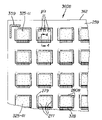
- FIG. 2A is a schematic plan view of a transparent cover plate configuration 250 A which does not have an inventive flow-preventing pattern.
- a transparent cover plate 252 has dispensed on a first surface 253 a plurality of drops or dots 270 of a flowable and curable adhesive material. Each drop or dot 270 contains an identical selected amount of the adhesive material.
- the adhesive material has a preferred viscosity in a range of from 50-1000 centipoise (cp), and can be obtained from, for example, Electronic Materials, Inc. of Breckenridge, Colo., U.S.A., or from Emerson & Cuming, Inc. of Billerica, Mass., U.S.A.
- the cover plate 252 includes an alignment mark 257 on the first cover plate surface 253 , and the drops or dots 270 are dispensed from a dispensing apparatus to form a two-dimensional array as indicated by x-direction and y-direction coordinates.
- the transparent cover plate can be a glass plate, a quartz plate, or a polymer plate such as, for example, a polycarbonate plate.
- FIG. 2B is a schematic plan view of an OLED device configuration 300 which includes a plurality of OLED devices formed in a two-dimensional array on a first surface 303 of a device substrate 302 .
- Each OLED device includes a pixelated display area 325 having picture elements or pixels “pix”, and one electrical interconnect area 328 .
- Neighbor OLED devices are separated by a spacing sx 1 along an x-direction and by a spacing sy 1 along a y-direction.
- Also formed on the first device substrate surface 303 is an alignment mark 357 .
- the pixelated structure of an OLED display area is indicated schematically within the display area of only one OLED device. Also, the positions of only three pixelated OLED display areas 325 within the two-dimensional array are indicated at 325 - 11 , corresponding to a position 1 ; 1 , 325 - 31 , corresponding to a position 3 ; 1 , and 325 - 14 , corresponding to a position 1 ; 4 .
- the pixelated display areas 325 can be those of passive matrix OLED devices, or the pixelated display areas can be associated with active matrix OLED devices.
- the drops or dots 270 of the flowable and curable adhesive material are dispensed in a pattern which corresponds to the positions of the OLED devices within the two-dimensional array. More particularly, the drops or dots 270 are dispensed so that their centers are approximately aligned with a center position of each OLED display area 325 , as indicated schematically by a dotted reference line (not identified) extending between FIGS. 2A and 2B .
- the curved arrows (not identified) shown between the cover plate configuration 250 A and the OLED device configuration 300 are intended to indicate the engagement of the cover plate's first surface 253 in alignment with the first surface 303 of the device substrate 302 .
- the surface 303 of the device substrate can be brought into aligned engagement with the first cover plate surface 253 .
- a video camera system monitors the positions of the alignment marks 257 and 357 at a proximity position between the cover plate configuration 250 A and the OLED device configuration 300 .
- One of these configurations is retained within a precision carriage such as, for example, a vacuum frame carriage, which can be translated manually or automatically in an x-direction, a y-direction, and a rotational direction to ensure alignment between the two configurations at engagement.
- a precision carriage such as, for example, a vacuum frame carriage, which can be translated manually or automatically in an x-direction, a y-direction, and a rotational direction to ensure alignment between the two configurations at engagement.
- a flowable and curable adhesive material is aimed at forming a transparent structural buffer layer (“SBL”) of radiation-cured adhesive material for uniformly bonding the cover plate configuration with at least the display areas 325 of each one of the OLED devices, while leaving at least the outermost portions of the electrical interconnect areas 328 clear of adhesive material.
- SBL transparent structural buffer layer
- FIG. 2C depicts schematically a plan view, viewed through the cover plate 252 , of an engaged and aligned assembly 360 A, and indicating aligned alignment marks 359 by shading, as well as common edges 362 of the aligned cover plate 252 with the device substrate 302 .
- the selected amount of flowable adhesive material dispensed as drops or dots 270 is shown to have been excessive since the unrestrained spread 275 of the drops or dots 270 by mere capillary action extends not only over the OLED display areas 325 as intended, but also over substantially the entire electrical interconnect areas 328 .
- Flow-preventing patterns provided in the form of dams are shown in bold outline.
- Flow-preventing patterns provided in the form of grooves are shown in fine outline.
- Flow-preventing patterns include a pattern of at least one dam feature on the cover plate or a pattern of at least one groove feature in the cover plate.
- Flow-preventing patterns using a dam feature can be included not only on the cover plate, but on the device substrate or other portions of the OLED devices, as will be apparent to those skilled in the art.
- FIGS. 3A and 3B schematic plan views are shown of a cover plate configuration 250 B which do have an inventive flow-preventing pattern and of an OLED device configuration 300 , respectively.
- the OLED device configuration 300 is identical with the configuration described with reference to FIG. 2B .
- the cover plate configuration 250 B has provided over a first surface 253 of a transparent cover plate 252 a plurality of rectilinear flow-preventing dam patterns 280 B, each pattern having one opening 281 .
- the dam patterns are provided in a dispensing apparatus (not shown) which dispenses a substantially viscous non-flowable and curable adhesive material having a viscosity in a preferred range of 25,000-250,000 centipoise (cp).
- cp centipoise
- the plurality of rectilinear dam patterns 280 B are arranged in a two-dimensional layout which corresponds to the two-dimensional array of OLED devices provided on the first surface 303 of the device substrate 302 .
- lower segments of the dam patterns 280 B align with such portions of the electrical interconnect areas 328 which are located in close proximity to the pixelated OLED display areas 325 .
- Upper segments of the dam patterns 280 B project to positions above upper edges (not identified in the drawings) of the pixelated OLED display areas 325 .
- a selected amount of a flowable and curable adhesive material is dispensed in the form of drops or dots 270 within each flow-preventing dam pattern 280 B.
- the flowable and curable adhesive material has been described with reference to FIG. 2A .
- inventive flow-preventing patterns in the form of dams or in the form of grooves is to prevent spreading of the flowable adhesive material into at least the outermost portions of the electrical interconnect areas 328 of the OLED devices, and to provide uniform spreading of the flowable adhesive material to a nearest edge or to nearest edges of the flow-preventing patterns so that, upon curing of the adhesive, a uniform transparent structural buffer layer provides uniform bonding between adhesive-containing areas of the cover plate 252 and at least the display areas 325 of each of the plurality of OLED devices on the device substrate 302 .
- FIG. 3C is a schematic plan view of an engaged and aligned assembly configuration 360 B as seen through the transparent cover plate 252 from the second cover plate surface 259 . Engaging the cover plate 252 with the device substrate occurs without externally applied forces.
- Controlled spreading of the flowable adhesive material is indicated at 277 , the spreading being controlled or confined by the flow-preventing dam patterns 280 B.
- the selected amount of the flowable adhesive material flows to spread to a nearest edge or to nearest edges of the flow-preventing pattern(s), and being prevented from flowing or spreading into the flow-preventing pattern(s) so that outermost portions of the electrical interconnect areas 328 remain free from any adhesive material.
- Overflow 279 of any excess amount of flowable adhesive material can take place through the opening(s) 281 (see FIG. 3A ) in the flow-preventing dam pattern 280 B.
- FIG. 4 is a schematic sectional view of a pixel “pix”, taken along the section lines 4 - 4 of the assembly configuration 360 B of FIG. 3C .
- a device substrate 302 has opposing first and second surfaces 303 and 305 , respectively.
- the pixel includes an anode electrode layer 304 formed on the first surface 303 of the device substrate 302 .
- the anode electrode layer 304 is in electrical contact with a metallized conductor (not identified) which is a portion of the electrical interconnect area 328 .
- An organic EL medium structure is provided over a portion of the anode electrode layer 304
- a cathode electrode layer 306 is provided over a portion of the EL medium structure.
- An electrical interconnect element or elements dedicated to the cathode electrode layer(s) is not shown in this drawing.
- a transparent encapsulation layer 310 fully encapsulates the pixel to provide an effective barrier against moisture penetration and oxygen penetration.
- the flow-preventing dam pattern 280 B is formed at a height dimension H to be in engagement with portions of the encapsulation layer 310 and with portions of the electrical interconnect area 328 .
- the dam pattern 280 B can also be included on the substrate.
- the dam pattern 280 B has been provided on the first surface 253 of the cover plate 252 , and the dam pattern provides for a uniform spacing 355 between the encapsulation layer 310 and the first cover plate surface 253 over the light-emitting portion “pix”. This uniform spacing is filled uniformly with the spread adhesive material 277 in a form of a controlled spread of drops or dots which is in fluid engagement with the cover plate surface 253 , and with an upper surface (not identified) of the encapsulation layer 310 .
- a second surface of the cover plate 252 is indicated at 259 .
- the height dimension H of the flow-preventing dam pattern 280 B is selected so that (1) the height dimension H extends vertically beyond topological features of the encapsulated OLED devices, and (2) the height dimension provides the uniform spacing 355 between the encapsulation layer 310 and the first cover plate surface 253 so that such uniform spacing can be filled uniformly with the spread adhesive material 277 .
- FIG. 5A is a schematic plan view of a cover plate configuration 250 C showing another embodiment of rectilinear flow-preventing dam patterns 280 C provided on a first surface 253 of a transparent cover plate 252 .
- Each dam pattern 280 C includes a continuous segment 280 C 1 extending along an x-direction, and interrupted darn segments 280 C 2 extending in an x-direction and a y-direction.
- the interrupted dam segments 280 C 2 provide a plurality of openings 283 .
- the continuous dam segment(s) 280 C 1 are positioned so as to align with such portions of electrical interconnect areas 328 which are in proximity to OLED display areas 325 , as indicated by a dotted reference line between FIG. 5A and FIG. 5B .
- FIG. 5B shows the configuration 300 of OLED devices having one electrical interconnect area, as described above with reference to FIG. 2B .
- Drops or dots 270 of a flowable and curable adhesive material are shown dispensed within each one of the plurality of flow-preventing patterns 280 C, as described with reference to FIG. 3A .
- FIG. 6 is a schematic plan view of a cover plate configuration 250 D showing another embodiment of rectilinear flow-preventing dam patterns 280 D provided on a first surface 253 of a transparent cover plate 252 or on the substrate.
- the dam pattern 280 D has a plurality of closed rectangular dams each of which has a drop 270 of a selected amount of a flowable and curable adhesive material dispensed within.
- a non-venting-type flow-preventing dam pattern such as rectilinear flow-preventing dam pattern 280 D, may require the assembly of the cover plate 252 to the device substrate be performed in a low pressure environment, e.g., 10 Pascal. Said low pressure environment will avoid entrapped gas preventing proper flow and spreading of drop 270 .
- FIG. 7 is a schematic plan view of a cover plate configuration 250 E showing another embodiment of rectilinear flow-preventing dam patterns 280 E provided on a first surface 253 of a transparent cover plate 252 .
- the dam pattern 280 E includes continuous dams 280 E 1 and perpendicular dam segments 280 E 2 which provide four openings 285 within each individual pattern.
- Each one of the plurality of darn patterns 280 E has a drop 270 of a selected amount of a flowable and curable adhesive material dispensed within.
- Both cover plate configurations 250 D and 250 E include an alignment mark 257 for aligning each of these cover plate configurations with respect to a device substrate in a manner described previously with reference to FIG. 3C .
- FIG. 8A is a schematic plan view of a cover plate configuration 250 F showing a plurality of interconnect area flow-preventing dam patterns 280 F provided on a first surface 253 of a transparent cover plate 252 .
- FIG. 8B shows the OLED device configuration 300 described previously with reference to FIG. 2B .
- the interconnect area flow-preventing dam patterns 280 F are positioned or arranged so that they align with respect to the electrical interconnect areas 328 of corresponding pixelated OLED devices, as indicated by dotted reference lines extending between FIG. 8A and FIG. 8B .
- Drops 270 of a selected amount of a flowable and curable adhesive material are dispensed at positions with respect to the patterns 280 F so that the drops establish fluid contact with an upper surface of an encapsulation layer (not identified) of respectively corresponding OLED display areas 325 , as is also indicated by a dotted reference line extending between FIG. 8A and FIG. 8B .
- FIG. 9A is a schematic plan view of a cover plate configuration 250 G showing a plurality of dual-interconnect area flow-preventing dam patterns 280 G provided on a first surface 253 of a transparent cover plate 252 or on the substrate.
- FIG. 9B is a schematic plan view of an OLED device configuration 300 - 2 in which each one of a plurality of OLED devices includes a pixelated display area and two electrical interconnect areas 328 and 329 .
- each flow-preventing pattern 280 G includes a first interconnect area flow-preventing dam pattern 280 G 1 to prevent spreading of a flowable and curable adhesive material into at least the outermost portions of a corresponding electrical interconnect area 328 , and a second interconnect area flow-preventing dam pattern 280 G 2 to prevent spreading of the flowable adhesive material into at least the outermost portions of a corresponding second electrical interconnect area 329 .
- a corresponding interconnect area flow-preventing dam pattern can be provided on the cover plate surface 253 or on the substrate.
- the OLED devices in device configuration 300 - 2 are shown having the same pixelated display areas 325 - 11 , 325 - 31 , and 325 - 14 as described above with reference to FIG. 2B . Therefore, the spacing sy 1 between neighbor devices in a y-direction remains, but the spacing sx 2 along an x-direction is reduced with respect to the spacing sx 1 by the introduction of the second electrical interconnect area 329 .
- Drops or dots 270 of a flowable and curable adhesive material are dispensed on the cover plate surface 253 in registration with the pattern 280 G, and in a manner described with reference to FIG. 2A and FIG. 3A .
- FIG. 10A is a schematic plan view of a cover plate configuration 250 H showing a plurality of sets of two unidirectional flow-preventing dam patterns 280 H, and a unidirectionally dispensed line or bead of a flowable and curable adhesive material formed between neighbor sets of the dam patterns 280 H.
- FIG. 10B shows the OLED device configuration 300 described previously with reference to FIG. 2B .
- one unidirectional flow-preventing dam of the set aligns with such portions of the OLED electrical interconnect areas 328 which are located in proximity to corresponding OLED display areas 325 .
- the other unidirectional flow-preventing dam of the set aligns in spaced relationship with edges of the display areas 325 which are located opposite the interconnect areas 328 .
- the unidirectionally dispensed lines or beads 272 align with the pixelated display areas 325 and extend along an x-direction across and between such display areas.
- a height dimension H of the flow-preventing dam patterns is selected on the basis of topological features of the OLED devices.
- An amount of the flowable adhesive material 277 is then selected to be dispensed, such selected amount, in turn, corresponding to the selected height dimension H.
- the flowable adhesive material 277 spreads laterally until the spreading stops at the inner edge or at the inner edges of the flow-preventing dam pattern(s).
- Spreading of the flowable adhesive material can be facilitated by concurrently engaging and heating the cover plate 252 and the device substrate 302 to a temperature in a range from 40-80° C. Such temperature is insufficient to cause thermally-induced curing of the adhesive materials.
- the flow-preventing dam patterns can be formed on the device substrate 102 , and the flowable adhesive material can be dispensed into the flow-preventing dam patterns formed on the device substrate.
- the flowable adhesive material can be dispensed on the cover plate in registration with the flow-preventing dam patterns formed on the device substrate.
- FIGS. 11 , 12 , and 13 A show flow-preventing patterns provided in the form of grooves which can be made to extend partially into a transparent cover plate 252 from a cover plate surface 253 .
- Grooves and groove configurations can be made, for example, by machining or by etching through openings in an overcoated and patterned photoresist layer which is subsequently removed.
- groove patterns can be effective flow-preventing patterns if (1) the grooves have sharp edges preferably without chips or imperfections at the first cover plate surface 253 ; and (2) a groove depth is a minimum of 50 micrometers but more preferably 300 micrometers; and (3) a groove width is a minimum of 0.5 mm but more preferably 1.0 mm.
- surfaces within the groove are preferably smooth and possess surface tension characteristics that do not facilitate the wetting of the flowable and curable adhesive material.
- FIG. 11 is a schematic plan view of a cover plate configuration 250 I showing a plurality of rectilinear flow-preventing groove patterns 280 I, depicted in dashed outline along lateral centers of the grooves that may also define the location of the OLED device edges for singulation.
- Each flow-preventing groove pattern 280 I includes interconnect area flow-preventing grooves 280 I 1 ; flow-preventing grooves 280 I 2 ; and flow-preventing grooves 280 I 3 .
- Flow-preventing grooves 280 I 2 also prevent spreading of the flowable adhesive material into the electrical interconnect area(s) from spreading adhesive material contained in vertically adjacent rows of OLED devices.
- a selected amount of a flowable and curable adhesive material is dispensed in the form of drops or dots 270 within each groove pattern 280 I.
- FIG. 12 is a schematic plan view of a cover plate configuration 250 J showing another embodiment of a flow-preventing groove pattern 280 J, indicated schematically in dashed outline along lateral centers of this unidirectional pattern which includes grooves 280 J 1 and grooves 280 J 2 .
- Grooves 280 J 1 are interconnect area flow-preventing grooves which can also serve as singulation markers for cover plate singulation over device interconnect areas. Grooves 280 J 2 are flow-preventing grooves which can also serve as singulation markers for device substrate singulation and for cover plate singulation.
- a selected amount of a flowable and curable adhesive material is dispensed in the form of a unidirectional line or bead 272 within each groove pattern 280 J.
- FIG. 13A and FIG. 13B schematic plan views are shown of a cover plate configuration 250 K and of an alternative OLED device configuration 300 A, respectively.
- the alternative OLED device configuration 300 A includes a plurality of OLED devices which are provided over a first surface 303 of a device substrate 302 .
- Each OLED device includes a pixelated (not identified in this drawing) display area 325 and an electrical interconnect area 328 .
- Three display areas are indicated at 325 - 11 , 325 - 21 , and 325 - 13 .
- An alternative alignment mark 367 is provided on the first surface 303 .
- the spacing between neighbor OLED devices along an x-direction and along a y-direction is shown reduced, compared to the previously described OLED device configuration 300 .
- the spacing sy 2 is substantially smaller than the spacing sy 1 of configuration 300
- the spacing sx 3 is shown to be less than the spacing sx 1 of configuration 300 .
- the cover plate configuration 250 K includes a unidirectional flow-preventing groove pattern 280 K which comprises relatively wide parallel single grooves.
- An alternative alignment mark 267 is provided on the first surface 253 of the cover plate 252 .
- a selected amount of a flowable and curable adhesive material is dispensed in the form of drops or dots 270 between grooves 280 K and in correspondence with positions of display areas 325 of the OLED devices in the device configuration 300 A.
- the positional relationships between the OLED devices and the grooves 280 K, and with the drops 270 is depicted by dotted reference lines extending between FIG. 13A and FIG. 13B .
- FIG. 14A-14C are schematic sectional views of a cover plate 252 having opposing first and second surfaces 253 and 259 , respectively, and showing groove patterns extending partially into the cover plate from the first surface 253 .
- FIG. 14A depicts the grooves 280 I 3 of the groove pattern 280 I of FIG. 11 .
- FIG. 14B shows the grooves 280 I 1 and 280 I 2 of the groove pattern 280 I of FIG. 11 .
- FIG. 14C indicates a groove 280 K of the unidirectional groove pattern of FIG. 13A .
- FIG. 15 a preferred curing process is indicated schematically in curing the spread adhesive material 277 in a form of controlled spread of drops or dots of the engaged and aligned assembly configuration 360 B of FIG. 3C .
- Curing radiation 700 is directed at the second surface 259 of the transparent cover plate 252 (see FIG. 3A ). At least a fraction of the curing radiation 700 is transmitted through the cover plate for impinging on the adhesive material and curing it to provide a structural buffer layer extending at least over the display area 325 of each OLED device.
- the cured adhesive layer e.g., the structural buffer layer, is designated at 277 c .
- the structural buffer layer 277 c can have a thickness in a range of from 1-50 micrometer.
- the curing radiation 700 cures the flow-preventing dam patterns 280 B to provide a cured dam pattern 280 Bc.
- curing of both the flowable adhesive material and the substantially viscous adhesive material forming the flow-preventing dam patterns is achieved by using curing radiation which includes a spectral distribution extending into the near-ultraviolet region.
- spectral sensitizing materials can be incorporated into radiation-responsive materials such as, for example, photoresist materials, so as to extend the radiation response of such materials into the visible region of the spectrum.
- sensitizing materials which bleach while being exposed to radiation in a spectral region including blue light in a wavelength range of 400-500 nm.
- An exemplary class of sensitizing materials useful in extending the spectral range of curing radiation into a blue light wavelength range of 400-450 nm includes keto-coumarin materials. Accordingly, curing the adhesive materials in the assembly 360 B is not restricted to using curing radiation 700 having the spectral distribution extending into the near-ultraviolet region.
- FIG. 16 a schematic perspective view is shown of a singulated packaged OLED device 360 Bs having the structural buffer layer in the form of the cured adhesive material 277 c and disposed within the cured flow-preventing dam pattern 280 Bc.
- the singulated device substrate 302 s and the singulated transparent cover plate 252 s share common singulated dimensions along three edges.
- the singulation of the cover plate is offset laterally with respect to the device substrate along the interconnect area.
- First and second surfaces 303 and 305 , respectively, of the singulated device substrate 302 s are shown. Also indicated is the second surface 259 of the singulated transparent cover plate 252 s.
- Light emission 390 from a pixel is directed toward an observer through the cover plate and its second surface 259 .
- Light emission, of any one pixel at an instant of time occurs in response to electrical drive signals and electrical control signals provided at the electrical interconnect area 328 by electrical leads 528 connected there to.
- Electrical leads 528 are the output leads issuing from an output terminal 510 of a power supply, scan line generator, and signal processor 500 which, in turn, receives an input signal at an input terminal 504 via a signal lead 502 .
- the pixelated display area 325 - xy (and its associated electrical interconnect area 328 ) can be that of any of the OLED devices singulated from the assembly 360 B of FIG. 15 .
- the inventive method can be used equally effectively to bond a transparent cover plate over a plurality of encapsulated bottom-emitting OLED devices formed on a surface of a transparent device substrate.
- Such bottom-emitting OLED devices can be active matrix or passive matrix devices.
- the cover plate is transparent so that curing radiation can be transmitted through the cover plate for curing the spread adhesive material and flow-preventing dam pattern(s), thereby forming the structural buffer layer.
- FIG. 17 is a flow chart indicating major process elements of the invention.
- Element 610 includes providing a device substrate having a plurality of OLED devices formed thereon.
- Element 620 includes providing a transparent cover plate.
- Element 630 includes providing a plurality of flow-preventing patterns on a surface of the cover plate.
- Element 640 includes dispensing a selected amount of flowable and curable adhesive material in a spatial relationship with each flow-preventing pattern.
- Element 650 includes engaging the cover plate in alignment with the device substrate and spreading the flowable adhesive material.
- Element 660 includes curing the spread adhesive material to provide uniform bonding between selected areas of the device substrate and the cover plate.
- Element 670 includes singulating the device substrate and the cover plate. In element 680 , individual OLED devices are obtained having a cover plate bonded by a structural buffer layer. The process ends at 690 .
Landscapes
- Physics & Mathematics (AREA)
- Optics & Photonics (AREA)
- Electroluminescent Light Sources (AREA)
Abstract
Description
- 1) increasing the aperture ratio, therefore permitting pixels of the display to operate at a lower current density which results in improved operational stability;
- 2) permitting more complex drive circuitry to enable improved control of pixel current, leading to enhanced display uniformity and to improved display stability;
- 3) enabling the use of lower mobility materials, e.g., amorphous silicon, to be considered in forming the thin-film transistor (TFT) drive circuitry; and
- 4) permitting incorporation of elements which can increase the out-coupling of light generated within the organic EL medium structure to provide increased efficiency of emitted light.
- 100 conventionally packaged OLED device (prior art)
- 102 device substrate
- 104 anode electrode layer
- 106 cathode electrode layer
- 124 anode(s) electrical interconnect area
- 126 cathode(s) electrical interconnect area
- 130 perimeter seal
- 140 desiccant material
- 150 cover plate
- 155 spacing or a gap between upper surface of cathode electrode layer (106) and lower surface of cover plate (150)
- 250 cover plate configuration
- 250A cover plate configuration without flow-preventing pattern
- 250B cover plate configuration with a first flow-preventing dam pattern
- 250C cover plate configuration with a second flow-preventing dam pattern
- 250D cover plate configuration with a third flow-preventing dam pattern
- 250E cover plate configuration with a fourth flow-preventing dam pattern
- 250F cover plate configuration with a fifth flow-preventing dam pattern
- 250G cover plate configuration with a sixth flow-preventing dam pattern
- 250H cover plate configuration with a seventh flow-preventing dam pattern
- 250I cover plate configuration with an eighth flow-preventing groove pattern
- 250J cover plate configuration with an ninth flow-preventing groove pattern
- 205K cover plate configuration with an tenth flow-preventing groove pattern
- 252 cover plate
- 252 s singulated portion of cover plate
- 253 first surface of cover plate (252)
- 257 alignment mark(s) on first cover plate surface (253)
- 259 second surface of cover plate (252)
- 267 alternative alignment mark(s) on first cover plate surface (253)
- 270 dispensed drops or dots of a flowable and curable adhesive material
- 272 dispensed lines of a flowable and curable adhesive material
- 275 unrestrained spread of drops or dots (270)
- 277 controlled spread of drops or dots (270)
- 277 c cured adhesive layer, or structural buffer layer (“SBL”)
- 279 overflow of excess flowable adhesive material
- 280B rectilinear flow-preventing dam pattern(s) with one opening (281)
- 280Bc cured flow-preventing dam pattern (280B)
- 280C rectilinear flow-preventing dam pattern(s) with continuous dam segments (280C1) and interrupted dam segments (280C2) providing a plurality of openings (283)
- 280C1 continuous dam segment(s)
- 280C2 interrupted dam segment(s)
- 280D closed rectilinear flow-preventing dam pattern(s)
- 280E rectilinear flow-preventing dam pattern(s) with continuous dams (280E1) and perpendicular dam segments (280E2) providing four openings (285)
- 280E1 continuous dam(s)
- 280E2 perpendicular dam segment(s)
- 280F interconnect area flow-preventing dam pattern(s)
- 280G dual-interconnect area flow-preventing darn pattern(s)
- 280G1 first interconnect area (328) flow-preventing darn pattern(s)
- 280G2 second interconnect area (329) flow-preventing dam pattern(s)
- 280H unidirectional flow-preventing darn pattern(s)
- 280I rectilinear flow-preventing groove pattern(s)
- 280I1 interconnect area flow-preventing groove(s)
- 280I2 flow-preventing groove(s)
- 280I3 flow-preventing groove(s)
- 280J unidirectional flow-preventing groove pattern(s)
- 280J1 interconnect area flow-preventing groove(s)
- 280J2 flow-preventing groove(s)
- 280K unidirectional flow-preventing groove pattern(s)
- 281 opening in flow-preventing
dam pattern 280B - 283 plurality of openings in flow-preventing
darn pattern 280C - 285 four openings in flow-preventing
darn pattern 280E - 300 configuration of OLED devices with one electrical interconnect area
- 300A alternative configuration of OLED devices
- 300-2 configuration of OLED devices with two electrical interconnect areas
- 302 device substrate
- 302 s singulated device substrate
- 303 first surface of device substrate (302)
- 304 anode electrode layer
- 305 second surface of device substrate
- 306 cathode electrode layer
- 310 encapsulation layer
- 325 pixelated display area
- 325-11 pixelated OLED display area at a position (1;1)
- 325-13 pixelated OLED display area at a position (1;3)
- 325-14 pixelated OLED display area at a position (1;4)
- 325-21 pixelated OLED display area at a position (2;1)
- 325-31 pixelated OLED display area at a position (3;1)
- 325-xy pixelated OLED display area at a position (x;y)
- 328 outermost portion(s) of electrical interconnect area(s)
- 329 outermost portion(s) of second electrical interconnect area(s)
- 355 spacing between upper surface of encapsulation layer (310) and first surface (253) of cover plate (252)
- 357 alignment mark(s) on first surface (303) of device substrate (302)
- 359 aligned alignment marks (257 and 357)
- 360A engaged and aligned assembly configuration “A”
- 360B engaged and aligned assembly configuration “B”
- 360Bs singulated packaged OLED device (from
assembly configuration 360B) - 362 common edge(s) of aligned cover plate (252) and device substrate (302)
- 367 alternative alignment mark(s) on first surface (303) of device substrate
- 390 light emission from a pixel
- 500 power supply, scan line generator, and signal processor
- 502 signal lead
- 504 input terminal
- 510 output terminal
- 528 electrical leads
- 600 start of process
- 610 providing device substrate
- 620 providing transparent cover plate
- 630 providing flow-preventing pattern
- 640 dispensing flowable and curable adhesive material
- 650 engaging cover plate in alignment with device substrate
- 660 curing spread adhesive material
- 670 singulating device substrate and bonded cover plate
- 680 obtaining individual OLED devices having bonded cover plate
- 690 end of process
- 700 curing radiation
- EL organic electroluminescent (“EL”) medium structure
- H height dimension of flow-preventing dam pattern(s)
- pix light-emitting portion of a pixel
- sx1 spacing between OLED devices along an x-direction
- sx2 spacing between OLED devices along an x-direction, where sx2<sx1
- sx3 spacing between OLED devices along an x-direction, where sx3<sx1
- sy1 spacing between OLED devices along a y-direction
- sy2 spacing between OLED devices along a y-direction where sy2<<sy1
- x x-direction
- y y-direction
Claims (16)
Priority Applications (1)
| Application Number | Priority Date | Filing Date | Title |
|---|---|---|---|
| US10/759,914 US7279063B2 (en) | 2004-01-16 | 2004-01-16 | Method of making an OLED display device with enhanced optical and mechanical properties |
Applications Claiming Priority (1)
| Application Number | Priority Date | Filing Date | Title |
|---|---|---|---|
| US10/759,914 US7279063B2 (en) | 2004-01-16 | 2004-01-16 | Method of making an OLED display device with enhanced optical and mechanical properties |
Publications (2)
| Publication Number | Publication Date |
|---|---|
| US20050155704A1 US20050155704A1 (en) | 2005-07-21 |
| US7279063B2 true US7279063B2 (en) | 2007-10-09 |
Family
ID=34749797
Family Applications (1)
| Application Number | Title | Priority Date | Filing Date |
|---|---|---|---|
| US10/759,914 Expired - Lifetime US7279063B2 (en) | 2004-01-16 | 2004-01-16 | Method of making an OLED display device with enhanced optical and mechanical properties |
Country Status (1)
| Country | Link |
|---|---|
| US (1) | US7279063B2 (en) |
Cited By (13)
| Publication number | Priority date | Publication date | Assignee | Title |
|---|---|---|---|---|
| US20080149380A1 (en) * | 2004-09-28 | 2008-06-26 | Rohm Co., Ltd. | Material Board for Producing Hybrid Circuit Board with Metallic Terminal Plate and Method for Producing Hybrid Circuit Board |
| US20090267891A1 (en) * | 2008-04-25 | 2009-10-29 | Bamidele Ali | Virtual paper |
| US20100107214A1 (en) * | 2008-10-27 | 2010-04-29 | Ganz | Temporary user account for a virtual world website |
| US20140346477A1 (en) * | 2013-05-24 | 2014-11-27 | Innolux Corporation | Organic light emitting display device |
| US20140346476A1 (en) * | 2013-05-24 | 2014-11-27 | Boe Technology Group Co., Ltd. | Oled display panel and the packaging method thereof, display device |
| CN104183614A (en) * | 2013-05-24 | 2014-12-03 | 群创光电股份有限公司 | Organic light emitting display device |
| WO2015180343A1 (en) * | 2014-05-29 | 2015-12-03 | 京东方科技集团股份有限公司 | Light-emitting display panel and manufacturing method therefor |
| US9978820B2 (en) * | 2015-12-31 | 2018-05-22 | Lg Display Co., Ltd. | Organic light emitting display device having a triple dam structure |
| US20190036234A1 (en) * | 2017-07-25 | 2019-01-31 | Lockheed Martin Corporation | Cable with nanoparticle paste |
| US20190234864A1 (en) * | 2013-12-12 | 2019-08-01 | G.M.S Global Mobile Solutions Ltd. | Sample holder for home testing device |
| CN110910777A (en) * | 2019-05-29 | 2020-03-24 | 友达光电股份有限公司 | Light emitting diode panel and splicing display device |
| US20230158888A1 (en) * | 2020-07-14 | 2023-05-25 | Japan Display Inc. | Display device |
| US20250261341A1 (en) * | 2024-02-11 | 2025-08-14 | Bizlink International Corp. | Small form factor transceiver module |
Families Citing this family (47)
| Publication number | Priority date | Publication date | Assignee | Title |
|---|---|---|---|---|
| DE112005000839B4 (en) * | 2004-04-22 | 2019-01-17 | Osram Oled Gmbh | Encapsulation for an organic electronic component and use |
| JP2006049308A (en) * | 2004-08-04 | 2006-02-16 | Samsung Electronics Co Ltd | Display device, manufacturing method thereof, and manufacturing device thereof |
| EP1655790B1 (en) * | 2004-10-21 | 2010-08-04 | LG Display Co., Ltd. | Organic electroluminescent device and method of manufacturing the same |
| US7843134B2 (en) * | 2005-10-31 | 2010-11-30 | Idemitsu Kosan Co., Ltd. | Organic EL emission devices connected in series |
| KR100685853B1 (en) * | 2006-01-25 | 2007-02-22 | 삼성에스디아이 주식회사 | Organic light emitting display device and manufacturing method |
| KR100801623B1 (en) * | 2006-06-23 | 2008-02-11 | 삼성전자주식회사 | Method for manufacturing display device, apparatus for manufacturing display device used therefor, and display device manufactured thereby |
| US20080216952A1 (en) * | 2007-03-06 | 2008-09-11 | Cheng Uei Precision Industry Co., Ltd. | Adhesive Method Of Optical Components |
| WO2009094558A2 (en) * | 2008-01-24 | 2009-07-30 | Brewer Science Inc. | Method for reversibly mounting a device wafer to a carrier substrate |
| WO2009099425A2 (en) * | 2008-02-07 | 2009-08-13 | Qd Vision, Inc. | Flexible devices including semiconductor nanocrystals, arrays, and methods |
| KR100953654B1 (en) | 2008-06-26 | 2010-04-20 | 삼성모바일디스플레이주식회사 | OLED display and manufacturing method thereof |
| JP5513020B2 (en) * | 2009-06-19 | 2014-06-04 | パナソニック液晶ディスプレイ株式会社 | THIN FILM TRANSISTOR SUBSTRATE AND METHOD FOR PRODUCING THIN FILM TRANSISTOR SUBSTRATE |
| WO2011047385A1 (en) | 2009-10-17 | 2011-04-21 | Qd Vision, Inc. | An optical, component, products including same, and methods for making same |
| KR101100955B1 (en) * | 2010-03-11 | 2011-12-29 | 삼성모바일디스플레이주식회사 | Organic light emitting display device and manufacturing method |
| KR101146994B1 (en) * | 2010-06-10 | 2012-05-22 | 삼성모바일디스플레이주식회사 | A display apparatus and a method for manufacturing the same |
| US8852391B2 (en) | 2010-06-21 | 2014-10-07 | Brewer Science Inc. | Method and apparatus for removing a reversibly mounted device wafer from a carrier substrate |
| US9263314B2 (en) | 2010-08-06 | 2016-02-16 | Brewer Science Inc. | Multiple bonding layers for thin-wafer handling |
| SG179299A1 (en) * | 2010-09-13 | 2012-04-27 | Trimech Technology Pte Ltd | A display panel substrate assembly, an apparatus and a method for forming a display panel substrate assembly |
| KR102037700B1 (en) | 2012-05-23 | 2019-10-30 | 삼성디스플레이 주식회사 | Portable display device and method of assembling the same |
| US9608029B2 (en) * | 2013-06-28 | 2017-03-28 | Stmicroelectronics Pte Ltd. | Optical package with recess in transparent cover |
| KR20150025994A (en) * | 2013-08-30 | 2015-03-11 | 엘지디스플레이 주식회사 | Organic light emitting diode display device and method of fabricating the same |
| WO2015116951A2 (en) | 2014-01-31 | 2015-08-06 | Canon U.S.A., Inc. | Optical probe, light intensity detection, imaging method and system |
| CN106028909B (en) | 2014-01-31 | 2019-05-17 | 佳能美国公司 | Device for color endoscopy |
| EP2960962B1 (en) | 2014-06-25 | 2020-04-01 | LG Display Co., Ltd. | Organic light emitting display apparatus |
| CN104461203B (en) * | 2014-12-22 | 2017-10-27 | 合肥鑫晟光电科技有限公司 | Cover plate and the film adhered method of touch-control sensing and touch-screen |
| CN104659269B (en) * | 2015-02-06 | 2017-05-17 | 深圳市华星光电技术有限公司 | OLED encapsulation method and OLED encapsulation structure |
| US10194065B2 (en) | 2015-08-05 | 2019-01-29 | Canon U.S.A., Inc. | Endoscope probes and systems, and methods for use therewith |
| US10966597B2 (en) | 2015-08-05 | 2021-04-06 | Canon U.S.A., Inc. | Forward and angle view endoscope |
| US9869854B2 (en) * | 2015-12-16 | 2018-01-16 | Canon U.S.A, Inc. | Endoscopic system |
| JP2019502519A (en) | 2015-12-28 | 2019-01-31 | キヤノン ユーエスエイ, インコーポレイテッドCanon U.S.A., Inc | Optical probe, light intensity detection, imaging method and system |
| US10551245B2 (en) | 2016-02-12 | 2020-02-04 | Canon U.S.A., Inc. | Simple monolithic optical element for forward-viewing spectrally encoded endoscopy |
| US10321810B2 (en) | 2016-06-13 | 2019-06-18 | Canon U.S.A., Inc. | Spectrally encoded endoscopic probe having a fixed fiber |
| KR102610024B1 (en) * | 2016-06-16 | 2023-12-06 | 삼성디스플레이 주식회사 | Display device |
| US10401610B2 (en) | 2016-07-15 | 2019-09-03 | Canon Usa, Inc. | Spectrally encoded probe with multiple diffraction orders |
| US10234694B2 (en) | 2016-07-15 | 2019-03-19 | Canon U.S.A., Inc. | Spectrally encoded probes |
| KR102284835B1 (en) | 2016-08-26 | 2021-07-30 | 몰레큘러 임프린츠 인코퍼레이티드 | Edge sealant confinement and halo reduction for optical devices |
| JP2019534069A (en) | 2016-09-23 | 2019-11-28 | キヤノン ユーエスエイ, インコーポレイテッドCanon U.S.A., Inc | Spectral-coded endoscopy apparatus and method |
| US10898068B2 (en) | 2016-11-01 | 2021-01-26 | Canon U.S.A., Inc. | Multi-bandwidth spectrally encoded endoscope |
| JP2018094395A (en) | 2016-11-03 | 2018-06-21 | キヤノン ユーエスエイ, インコーポレイテッドCanon U.S.A., Inc | Diagnostic spectrally encoded endoscopy apparatus and system, and methods for use therewith |
| KR102795249B1 (en) * | 2017-02-14 | 2025-04-14 | 삼성디스플레이 주식회사 | Display device and manufacturing method of the same |
| US10825152B2 (en) | 2017-09-14 | 2020-11-03 | Canon U.S.A., Inc. | Distortion measurement and correction for spectrally encoded endoscopy |
| KR102360094B1 (en) * | 2017-09-15 | 2022-02-09 | 삼성디스플레이 주식회사 | Display device |
| WO2019241398A1 (en) | 2018-06-12 | 2019-12-19 | Wendong Xing | Edge sealant application for optical devices |
| CN117310920A (en) | 2018-07-23 | 2023-12-29 | 奇跃公司 | Optical device vent gaps for edge sealants and laminate dams |
| CN115625829A (en) | 2018-10-16 | 2023-01-20 | 奇跃公司 | A method of forming a waveguide portion having a predetermined shape |
| CN109542269B (en) * | 2018-11-20 | 2022-05-03 | 信利(惠州)智能显示有限公司 | Touch display screen and touch display device |
| CN113471256B (en) * | 2021-06-16 | 2023-04-18 | 武汉华星光电技术有限公司 | Display panel and preparation method thereof |
| CN114078396A (en) * | 2021-11-30 | 2022-02-22 | 云谷(固安)科技有限公司 | Bonding method and bonding apparatus |
Citations (12)
| Publication number | Priority date | Publication date | Assignee | Title |
|---|---|---|---|---|
| US4657341A (en) * | 1983-08-03 | 1987-04-14 | Siemens Aktiengesellschaft | Connector for light waveguides and method of producing same |
| US6198217B1 (en) * | 1997-05-12 | 2001-03-06 | Matsushita Electric Industrial Co., Ltd. | Organic electroluminescent device having a protective covering comprising organic and inorganic layers |
| US6268695B1 (en) | 1998-12-16 | 2001-07-31 | Battelle Memorial Institute | Environmental barrier material for organic light emitting device and method of making |
| US20020074931A1 (en) * | 2000-12-20 | 2002-06-20 | Koninklijke Philips Electronics N.V. | Device, particularly an electroluminescent display device, and method of manufacturing such a device |
| US20020155320A1 (en) | 2001-04-20 | 2002-10-24 | Lg.Philips Lcd Co., Ltd. | Organic electroluminescent device |
| US20020187775A1 (en) | 1999-12-13 | 2002-12-12 | Louis Corrigan | WAP service personalisation, management and billing object oriented platform |
| US20020193035A1 (en) | 2001-06-14 | 2002-12-19 | Mao-Kuo Wei | Package method and apparatus for organic electro-luminescent display |
| US20030067268A1 (en) * | 2001-09-28 | 2003-04-10 | Hideki Matsuoka | Method of manufacturing electroluminescence panel |
| US20030218442A1 (en) * | 2002-05-25 | 2003-11-27 | Motorola, Inc. | Methods and devices for controlling stepper motors |
| US20030218422A1 (en) * | 2002-05-23 | 2003-11-27 | Samsung Sdi Co., Ltd. | Method for encapsulating organic electroluminescent device and an organic electroluminescent panel using the same |
| US20050002081A1 (en) * | 2001-09-14 | 2005-01-06 | Fabien Beteille | Functional safety glazing unit |
| US6867539B1 (en) * | 2000-07-12 | 2005-03-15 | 3M Innovative Properties Company | Encapsulated organic electronic devices and method for making same |
-
2004
- 2004-01-16 US US10/759,914 patent/US7279063B2/en not_active Expired - Lifetime
Patent Citations (12)
| Publication number | Priority date | Publication date | Assignee | Title |
|---|---|---|---|---|
| US4657341A (en) * | 1983-08-03 | 1987-04-14 | Siemens Aktiengesellschaft | Connector for light waveguides and method of producing same |
| US6198217B1 (en) * | 1997-05-12 | 2001-03-06 | Matsushita Electric Industrial Co., Ltd. | Organic electroluminescent device having a protective covering comprising organic and inorganic layers |
| US6268695B1 (en) | 1998-12-16 | 2001-07-31 | Battelle Memorial Institute | Environmental barrier material for organic light emitting device and method of making |
| US20020187775A1 (en) | 1999-12-13 | 2002-12-12 | Louis Corrigan | WAP service personalisation, management and billing object oriented platform |
| US6867539B1 (en) * | 2000-07-12 | 2005-03-15 | 3M Innovative Properties Company | Encapsulated organic electronic devices and method for making same |
| US20020074931A1 (en) * | 2000-12-20 | 2002-06-20 | Koninklijke Philips Electronics N.V. | Device, particularly an electroluminescent display device, and method of manufacturing such a device |
| US20020155320A1 (en) | 2001-04-20 | 2002-10-24 | Lg.Philips Lcd Co., Ltd. | Organic electroluminescent device |
| US20020193035A1 (en) | 2001-06-14 | 2002-12-19 | Mao-Kuo Wei | Package method and apparatus for organic electro-luminescent display |
| US20050002081A1 (en) * | 2001-09-14 | 2005-01-06 | Fabien Beteille | Functional safety glazing unit |
| US20030067268A1 (en) * | 2001-09-28 | 2003-04-10 | Hideki Matsuoka | Method of manufacturing electroluminescence panel |
| US20030218422A1 (en) * | 2002-05-23 | 2003-11-27 | Samsung Sdi Co., Ltd. | Method for encapsulating organic electroluminescent device and an organic electroluminescent panel using the same |
| US20030218442A1 (en) * | 2002-05-25 | 2003-11-27 | Motorola, Inc. | Methods and devices for controlling stepper motors |
Cited By (29)
| Publication number | Priority date | Publication date | Assignee | Title |
|---|---|---|---|---|
| US7943860B2 (en) * | 2004-09-28 | 2011-05-17 | Rohm Co., Ltd. | Material board for producing hybrid circuit board with metallic terminal plate and method for producing hybrid circuit board |
| US20080149380A1 (en) * | 2004-09-28 | 2008-06-26 | Rohm Co., Ltd. | Material Board for Producing Hybrid Circuit Board with Metallic Terminal Plate and Method for Producing Hybrid Circuit Board |
| US20090267891A1 (en) * | 2008-04-25 | 2009-10-29 | Bamidele Ali | Virtual paper |
| US20100107214A1 (en) * | 2008-10-27 | 2010-04-29 | Ganz | Temporary user account for a virtual world website |
| US8516553B2 (en) | 2008-10-27 | 2013-08-20 | Ganz | Temporary user account for a virtual world website |
| US8826383B2 (en) | 2008-10-27 | 2014-09-02 | Ganz | Temporary user account for a virtual world website |
| CN104183614B (en) * | 2013-05-24 | 2017-06-06 | 群创光电股份有限公司 | Organic Light Emitting Display Device |
| US20140346477A1 (en) * | 2013-05-24 | 2014-11-27 | Innolux Corporation | Organic light emitting display device |
| US20140346476A1 (en) * | 2013-05-24 | 2014-11-27 | Boe Technology Group Co., Ltd. | Oled display panel and the packaging method thereof, display device |
| CN104183614A (en) * | 2013-05-24 | 2014-12-03 | 群创光电股份有限公司 | Organic light emitting display device |
| US8969904B2 (en) * | 2013-05-24 | 2015-03-03 | Innolux Corporation | Organic light emitting display device |
| US10935484B2 (en) | 2013-12-12 | 2021-03-02 | Mes Medical Electronic Systems Ltd. | Automated assessment of sperm samples |
| US20190234864A1 (en) * | 2013-12-12 | 2019-08-01 | G.M.S Global Mobile Solutions Ltd. | Sample holder for home testing device |
| US10859488B2 (en) * | 2013-12-12 | 2020-12-08 | Mes Medical Electronic Systems Ltd. | Sample holder for home testing device |
| WO2015180343A1 (en) * | 2014-05-29 | 2015-12-03 | 京东方科技集团股份有限公司 | Light-emitting display panel and manufacturing method therefor |
| US9985244B2 (en) | 2014-05-29 | 2018-05-29 | Boe Technology Group Co., Ltd. | Light emitting display panel and manufacturing method thereof |
| US9502678B2 (en) | 2014-05-29 | 2016-11-22 | Boe Technology Group Co., Ltd. | Light emitting display panel and manufacturing method thereof |
| US10916604B2 (en) | 2015-12-31 | 2021-02-09 | Lg Display Co., Ltd. | Organic light emitting display device having a multi-directional dam structure |
| US10304916B2 (en) | 2015-12-31 | 2019-05-28 | Lg Display Co., Ltd. | Organic light emitting display device having a non-display area dam structure |
| US9978820B2 (en) * | 2015-12-31 | 2018-05-22 | Lg Display Co., Ltd. | Organic light emitting display device having a triple dam structure |
| US11552141B2 (en) | 2015-12-31 | 2023-01-10 | Lg Display Co, Ltd. | Organic light emitting display device including curve-shaped third dam structure |
| US11968860B2 (en) | 2015-12-31 | 2024-04-23 | Lg Display Co., Ltd. | Organic light emitting display device including dam structure and alignment mark |
| US20190036234A1 (en) * | 2017-07-25 | 2019-01-31 | Lockheed Martin Corporation | Cable with nanoparticle paste |
| US11031704B2 (en) * | 2017-07-25 | 2021-06-08 | Lockheed Martin Corporation | Cable with nanoparticle paste |
| CN110910777A (en) * | 2019-05-29 | 2020-03-24 | 友达光电股份有限公司 | Light emitting diode panel and splicing display device |
| US11195970B2 (en) * | 2019-05-29 | 2021-12-07 | Au Optronics Corporation | Light emitting diode panel and tiling display apparatus |
| US20230158888A1 (en) * | 2020-07-14 | 2023-05-25 | Japan Display Inc. | Display device |
| US12533951B2 (en) * | 2020-07-14 | 2026-01-27 | Japan Display Inc. | Display device |
| US20250261341A1 (en) * | 2024-02-11 | 2025-08-14 | Bizlink International Corp. | Small form factor transceiver module |
Also Published As
| Publication number | Publication date |
|---|---|
| US20050155704A1 (en) | 2005-07-21 |
Similar Documents
| Publication | Publication Date | Title |
|---|---|---|
| US7279063B2 (en) | Method of making an OLED display device with enhanced optical and mechanical properties | |
| CN106876328B (en) | OLED display panel, preparation method thereof, and display device | |
| US7932670B2 (en) | Organic electro-luminescence display device and method of manufacturing the same | |
| CN207381403U (en) | Display base plate, display panel | |
| US7144752B2 (en) | Method of manufacturing organic electroluminescent display device and organic electroluminescent display device, and display device equipped with organic electroluminescent display device | |
| KR101301180B1 (en) | Dual Plate Type Organic Electro-luminescent Device and the method for | |
| CN108123062A (en) | Organic light-emitting display device | |
| US10276812B2 (en) | Display device and manufacturing method thereof | |
| JP2004342432A (en) | Organic EL display | |
| CN108172604A (en) | A kind of OLED encapsulating structures, packaging method, display device | |
| JP2008235089A (en) | Organic EL display panel and manufacturing method thereof | |
| CN100559626C (en) | Double-plate type organic electroluminescent display device and manufacturing method thereof | |
| US7135352B2 (en) | Method of fabricating a cover plate bonded over an encapsulated OLEDs | |
| CN108417598B (en) | OLED display panel, packaging method and preparation method of organic film | |
| KR102583813B1 (en) | Display apparatus | |
| KR100963073B1 (en) | Organic light emitting display device | |
| CN116234367A (en) | Display panel and method for manufacturing same | |
| KR102094143B1 (en) | Fabricating Method Of Organic Light Emitting Diode Display | |
| CN108666437B (en) | Display panel and manufacturing method thereof | |
| KR100703457B1 (en) | Organic electroluminescent display and manufacturing method thereof | |
| CN1967899B (en) | Organic electroluminescence display element and manufacturing method thereof | |
| KR100815761B1 (en) | Manufacturing method of organic electroluminescent display | |
| KR20240094208A (en) | Display device and method of manufacturing the same | |
| KR102873578B1 (en) | Organic light emitting display device | |
| CN112599433B (en) | Display panel binding method and display device |
Legal Events
| Date | Code | Title | Description |
|---|---|---|---|
| AS | Assignment |
Owner name: EASTMAN KODAK COMPANY, NEW YORK Free format text: ASSIGNMENT OF ASSIGNORS INTEREST;ASSIGNORS:YOKAJTY, JOSEPH E.;SERBICKI, JEFFREY P.;VANSLYKE, STEVEN A.;REEL/FRAME:014904/0569;SIGNING DATES FROM 20031215 TO 20031222 |
|
| FEPP | Fee payment procedure |
Free format text: PAYOR NUMBER ASSIGNED (ORIGINAL EVENT CODE: ASPN); ENTITY STATUS OF PATENT OWNER: LARGE ENTITY |
|
| STCF | Information on status: patent grant |
Free format text: PATENTED CASE |
|
| FEPP | Fee payment procedure |
Free format text: PAYER NUMBER DE-ASSIGNED (ORIGINAL EVENT CODE: RMPN); ENTITY STATUS OF PATENT OWNER: LARGE ENTITY Free format text: PAYOR NUMBER ASSIGNED (ORIGINAL EVENT CODE: ASPN); ENTITY STATUS OF PATENT OWNER: LARGE ENTITY |
|
| AS | Assignment |
Owner name: GLOBAL OLED TECHNOLOGY LLC,DELAWARE Free format text: ASSIGNMENT OF ASSIGNORS INTEREST;ASSIGNOR:EASTMAN KODAK COMPANY;REEL/FRAME:023998/0368 Effective date: 20100122 Owner name: GLOBAL OLED TECHNOLOGY LLC, DELAWARE Free format text: ASSIGNMENT OF ASSIGNORS INTEREST;ASSIGNOR:EASTMAN KODAK COMPANY;REEL/FRAME:023998/0368 Effective date: 20100122 |
|
| FPAY | Fee payment |
Year of fee payment: 4 |
|
| FPAY | Fee payment |
Year of fee payment: 8 |
|
| MAFP | Maintenance fee payment |
Free format text: PAYMENT OF MAINTENANCE FEE, 12TH YEAR, LARGE ENTITY (ORIGINAL EVENT CODE: M1553); ENTITY STATUS OF PATENT OWNER: LARGE ENTITY Year of fee payment: 12 |