US7256830B2 - Solid-state imaging device and manufacturing method for solid-state imaging device - Google Patents
Solid-state imaging device and manufacturing method for solid-state imaging device Download PDFInfo
- Publication number
- US7256830B2 US7256830B2 US10/438,331 US43833103A US7256830B2 US 7256830 B2 US7256830 B2 US 7256830B2 US 43833103 A US43833103 A US 43833103A US 7256830 B2 US7256830 B2 US 7256830B2
- Authority
- US
- United States
- Prior art keywords
- imaging device
- state imaging
- solid
- photoelectric conversion
- layered
- Prior art date
- Legal status (The legal status is an assumption and is not a legal conclusion. Google has not performed a legal analysis and makes no representation as to the accuracy of the status listed.)
- Expired - Fee Related, expires
Links
Images


Classifications
-
- H—ELECTRICITY
- H10—SEMICONDUCTOR DEVICES; ELECTRIC SOLID-STATE DEVICES NOT OTHERWISE PROVIDED FOR
- H10F—INORGANIC SEMICONDUCTOR DEVICES SENSITIVE TO INFRARED RADIATION, LIGHT, ELECTROMAGNETIC RADIATION OF SHORTER WAVELENGTH OR CORPUSCULAR RADIATION
- H10F39/00—Integrated devices, or assemblies of multiple devices, comprising at least one element covered by group H10F30/00, e.g. radiation detectors comprising photodiode arrays
- H10F39/10—Integrated devices
- H10F39/12—Image sensors
- H10F39/15—Charge-coupled device [CCD] image sensors
- H10F39/156—CCD or CID colour image sensors
-
- H—ELECTRICITY
- H10—SEMICONDUCTOR DEVICES; ELECTRIC SOLID-STATE DEVICES NOT OTHERWISE PROVIDED FOR
- H10F—INORGANIC SEMICONDUCTOR DEVICES SENSITIVE TO INFRARED RADIATION, LIGHT, ELECTROMAGNETIC RADIATION OF SHORTER WAVELENGTH OR CORPUSCULAR RADIATION
- H10F39/00—Integrated devices, or assemblies of multiple devices, comprising at least one element covered by group H10F30/00, e.g. radiation detectors comprising photodiode arrays
- H10F39/011—Manufacture or treatment of image sensors covered by group H10F39/12
- H10F39/014—Manufacture or treatment of image sensors covered by group H10F39/12 of CMOS image sensors
-
- H—ELECTRICITY
- H10—SEMICONDUCTOR DEVICES; ELECTRIC SOLID-STATE DEVICES NOT OTHERWISE PROVIDED FOR
- H10F—INORGANIC SEMICONDUCTOR DEVICES SENSITIVE TO INFRARED RADIATION, LIGHT, ELECTROMAGNETIC RADIATION OF SHORTER WAVELENGTH OR CORPUSCULAR RADIATION
- H10F39/00—Integrated devices, or assemblies of multiple devices, comprising at least one element covered by group H10F30/00, e.g. radiation detectors comprising photodiode arrays
- H10F39/011—Manufacture or treatment of image sensors covered by group H10F39/12
- H10F39/026—Wafer-level processing
-
- H—ELECTRICITY
- H10—SEMICONDUCTOR DEVICES; ELECTRIC SOLID-STATE DEVICES NOT OTHERWISE PROVIDED FOR
- H10F—INORGANIC SEMICONDUCTOR DEVICES SENSITIVE TO INFRARED RADIATION, LIGHT, ELECTROMAGNETIC RADIATION OF SHORTER WAVELENGTH OR CORPUSCULAR RADIATION
- H10F39/00—Integrated devices, or assemblies of multiple devices, comprising at least one element covered by group H10F30/00, e.g. radiation detectors comprising photodiode arrays
- H10F39/10—Integrated devices
- H10F39/12—Image sensors
- H10F39/15—Charge-coupled device [CCD] image sensors
- H10F39/151—Geometry or disposition of pixel elements, address lines or gate electrodes
-
- H—ELECTRICITY
- H10—SEMICONDUCTOR DEVICES; ELECTRIC SOLID-STATE DEVICES NOT OTHERWISE PROVIDED FOR
- H10F—INORGANIC SEMICONDUCTOR DEVICES SENSITIVE TO INFRARED RADIATION, LIGHT, ELECTROMAGNETIC RADIATION OF SHORTER WAVELENGTH OR CORPUSCULAR RADIATION
- H10F39/00—Integrated devices, or assemblies of multiple devices, comprising at least one element covered by group H10F30/00, e.g. radiation detectors comprising photodiode arrays
- H10F39/80—Constructional details of image sensors
- H10F39/806—Optical elements or arrangements associated with the image sensors
- H10F39/8063—Microlenses
Definitions
- This invention relates to a solid-state imaging device, more particularly to a solid-state imaging device having a CCD-type transfer channel.
- FIG. 9 is a block diagram showing a structure of a conventional four-phase drive ( ⁇ 1- ⁇ 4) charge coupled device (CCD) type solid-state imaging device 52 according to the prior art.
- CCD charge coupled device
- the solid-state imaging device 52 has an image area 60 a , a multiplicity of photodiodes 62 arranged in a tetragonal matrix, and a vertical charge coupled device (VCCD) 64 arranged in correspondence with each column of the photodiodes.
- the VCCD 64 has a multi-layered electrode structure as described later.
- a horizontal charge coupled device (HCCD) 60 b is configured at one end of the image area 60 a .
- the HCCD 60 b also has a multi-layered electrode structure similar to the VCCD 64 .
- an output amplifier 55 consisted of a high-speed analogue amplifier is configured.
- Signal charges stored in the photodiodes 62 are transferred to the VCCD 64 simultaneously, and thereafter the VCCD 64 transfers the signal charges in a vertical direction in order.
- the signal charges transferred by the VCCD 64 are transferred in a horizontal direction row by row by the HCCD 60 b and are output to the later-described analogue signal processing circuit 53 ( FIG. 11 ) after being amplified by the output amplifier 55 .
- the output amplifier 55 is formed, for example, by including a charge/voltage (Q/V) converter consisted of a floating diffusion amplifier (FDA) and a source follower circuit.
- Q/V charge/voltage
- the HCCD 60 b transfers the signal charges by using high-speed transfer pulse over 14 MHz or over, and so power consumption of the HCCD 60 b is high.
- the power consumption of the HCCD 60 b counts about 40% of a total power consumption of the solid-state imaging device 52 .
- power consumption of the output amplifier 55 also counts about 40% of the total power consumption of the solid-state imaging device 52 . Therefore, in the solid-state imaging device 52 according to the prior art, sum of the power consumption of the HCCD 60 b and the output amplifier 55 counts about 80% of the total power consumption.
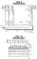
- FIG. 10 schematically shows a structure of a double-layered poly-silicon electrode that is an example of the multi-layered electrode structure according to the prior art.
- the VCCD 64 is formed, for example, by including a vertical transfer channel 614 made of an n-type impurity doped region formed on a p-well 611 b of a semiconductor substrate 611 a , an oxide film 615 a formed on the vertical transfer channel 614 , a first layer poly-silicon electrode 616 a formed on the oxide film 615 a , an inter-layer insulating film 615 b formed by oxidizing the first layer poly-silicon electrode 616 a , and a second layer poly-silicon electrode 616 b formed on the inter-layer insulating film 615 b and overlapping edge portions of the first layer poly-silicon electrode 616 a.
- the inter-layer insulating film 615 b is formed by oxidizing a surface of the first layer poly-silicon electrode 616 a .
- a Si surface exposing under the oxide silicon layer is also slightly oxidized.
- a film thickness of the oxide film 615 a under the second layer poly-silicon electrode 616 b will be thinner than a film thickness of the oxide film 615 a under the first layer poly-silicon electrode 616 a , and therefore, difference in the film thickness will be occurred.
- the film thickness of the oxide film 615 a has to be thick in advance. By making the film thickness thick, drive voltage of the electrode will be high. This point is a common feature of forming an inter-layer insulating film between laminated electrodes like the double-layered poly-silicon electrode shown in the drawing, a triple-layered poly-silicon electrode or the likes.
- FIG. 11 is a block diagram showing a structure of an imaging system of a digital camera using an analogue output solid-state imaging device.
- an analogue signal processing circuit 53 In an imaging system of a digital camera using a conventional solid-state imaging device, for example, an analogue signal processing circuit 53 , an analogue/digital converter (ADC) 54 , a digital signal processing circuit 63 , a system controlling unit 5 and a storage medium 6 are connected to a bus line 7 .
- ADC an analogue/digital converter
- a solid-state imaging device 52 is, for example, a CCD type solid-state imaging device shown in FIG. 9 .
- the solid-state imaging device 52 is connected to the analogue signal processing circuit 53 and supplies signal charges to the analogue signal processing circuit 53 .
- the system controlling unit 5 controls operations of the analogue signal processing circuit 53 , the ADC 54 , the digital signal processing circuit 63 , a DRAM 4 , and the storage medium 6 , all of which are connected to the bus line 7 .
- the analogue signal processing circuit 53 is consisted of, for example, a noise-eliminating unit made of a correlated double sampling circuit, a color signal processing circuit, etc.
- the ADC 54 converts analogue voltage signals into digital signals row by row and outputs them to the digital signal processing circuit 63 .
- the digital signal processing circuit 63 can stores the input digital signals into the DRAM 4 row by row. Also, the digital signal processing circuit 63 reads the digital signals stored in the DRAM 4 and executes various image signal processes such as JPEG compressing and decompressing, etc. Moreover, the digital signal processing circuit 63 outputs the image signal processed digital signals to a monitor and stores them into the storage medium 6 .
- FIT-CCD frame interline transfer
- charge signals are transferred vertically at a high-speed and stored temporarily into the charge storage region formed at one end of an image area before being transferred horizontally.
- the high-speed charge transfer of the vertical charge coupled devices (VCCD) in the FIT-CCD can reduce smear noise of a CCD image sensor.
- the HCCD 60 b and the output amplifier 55 As described in the above, about 80% of the total power consumption of the conventional CCD type solid-state imaging device 52 is used by the HCCD 60 b and the output amplifier 55 . For increasing the number of pixels, further high-speed driving of the HCCD 60 b and the output amplifier 55 will be necessary, and the power consumption will become higher.
- CCD type solid-state imaging device having two HCCDs for doubling a transfer rate at the same transfer clock frequency.
- the above-described FIT-CCD used a multi-layered poly-silicon electrode, it was difficult to drive a VCCD at a high-speed because of high resistance of poly-silicon.
- a metal lining structure is applied in order to lower the resistance, the FIT-CCD is used for a limited purpose such as a broadcasting system or the likes because of its difficulty in manufacturing and miniaturization.
- the FIT-CCD consume higher power than a normal CCD due to higher driving speed.
- a solid-state imaging device comprising: a semi-conductor substrate demarcating a two-dimensional surface; a multiplicity of photoelectric conversion units formed at grid points of a first grid of a first tetragonal matrix and a second tetragonal matrix having grid points between grid points of the first tetragonal matrix; a vertical transfer channel arranged in a vertical direction by weaving a space between the horizontally adjacent photoelectric conversion units; a plurality of single-layered electrodes formed above the vertical transfer channel and arranged in a horizontal direction by weaving a space between the vertically adjacent photoelectric conversion units; and a signal processor having a gate electrode and formed, in correspondence to the vertical transfer channel, at one end of the vertical transfer channel on the semiconductor substrate.
- a solid-state imaging device comprising: a semi-conductor substrate demarcating a two-dimensional surface; a multiplicity of photoelectric conversion units formed at grid points of a first grid of a first tetragonal matrix and a second tetragonal matrix having grid points between grid points of the first tetragonal matrix; a vertical transfer channel arranged in a vertical direction by weaving a space between the horizontally adjacent photoelectric conversion units; a plurality of single-layered electrodes formed above the vertical transfer channel and arranged in a horizontal direction by weaving a space between the vertically adjacent photoelectric conversion units; a charge storing unit formed, in correspondence to the vertical transfer channel, at one end of the vertical transfer channel on the semiconductor substrate; and a signal processor having a gate electrode and formed, in correspondence to the vertical transfer channel, at one end of the charge storing unit.
- a manufacturing method for a solid-state imaging device comprising the steps of: (a) preparing a semi-conductor substrate demarcating a two-dimensional surface; (b) forming, in an image area of the semiconductor substrate, a multiplicity of photoelectric conversion units at grid points of a first grid of a first tetragonal matrix and a second tetragonal matrix having grid points between grid points of the first tetragonal matrix; (c) forming a vertical transfer channel arranged in a vertical direction by weaving a space between the horizontally adjacent photoelectric conversion units; and (d) forming a plurality of single-layered electrodes crossing above the vertical transfer channel and extending in a horizontal direction by weaving a space between the vertically adjacent photoelectric conversion units, and forming a gate electrode of a signal processor at one end of the vertical transfer channel in correspondence to the vertical transfer channel.
- a CCD type solid-state imaging device with low power consumption can be provided.
- a CCD type solid-state imaging device with an on-chip peripheral circuit that can be easily manufactured can be provided.
- a FIT-CCD type solid-state imaging device that can be easily manufactured and miniaturized can be provided.
- FIG. 1 is a block diagram showing a structure of an imaging system of a digital camera 1 according to a first embodiment of the present invention.
- FIG. 2 is a block diagram showing a structure of a solid-state imaging device 2 according to the first embodiment of the present invention.
- FIG. 3 is an enlarged plan view showing a part of an image area 10 a of a solid-state imaging device according to the first embodiment of the present invention.
- FIG. 4 is a block diagram showing an example of a structure of a peripheral circuit (CMOS circuit) 10 b according to the first embodiment of the present invention.
- CMOS circuit peripheral circuit
- FIG. 5 is an enlarged cross sectional view of the solid-state imaging device 2 according to the first embodiment of the present invention.
- FIG. 6 is a flow chart showing a manufacturing process of the solid-state imaging device 2 according to the first embodiment of the present invention.
- FIG. 7 is a bar graph showing a power consumption of the solid-state imaging device 2 according to the first embodiment of the present invention.
- FIG. 8 is a block diagram showing a structure of a solid-state imaging device 2 according to a second embodiment of the present invention.
- FIG. 9 is a block diagram showing a structure of a CCD type solid-state imaging device 52 according to the prior art.
- FIG. 10 is a schematic cross sectional view showing a structure of a multi-layered electrode structure according to the prior art.
- FIG. 11 is a block diagram showing a structure of an imaging system of a digital camera using a solid-state imaging device according to the prior art.
- FIG. 1 is a block diagram showing a structure of an imaging system of a digital camera 1 according to a first embodiment of the present invention.
- a digital signal processing circuit 3 , a system controlling unit 5 and a storage medium 6 are connected to a bus line of the digital camera 1 .
- the digital signal processing circuit is formed by including a JPEG compression/decompression circuit, a DRAM controlling circuit, a DRAM, etc.
- the system controlling unit 5 writes digital data output from a solid-state imaging device 2 into the DRAM 4 and afterwards reads the digital data from the DRAM 4 in order to make the digital signal processing circuit 3 perform various image processes such as color conversion, gamma correction, JPEG compression/decompression, etc. Also, the system controlling unit 5 make the digital signal processing circuit 3 output the digital data to which the various imaging processes are performed to a monitor and store the digital data into the storage medium 6 formed of a semiconductor memory, etc. such as a flash memory or the likes. The system controlling unit 5 controls operations of the digital signal processing circuit 3 , the storage medium 6 or the likes.
- an output of the solid-state imaging device 2 is digital data; therefore, it is not necessary to have an analogue signal processing circuit and ADC outside of the solid-state imaging device 2 .
- FIG. 2 is a block diagram showing a structure of a solid-state imaging device 2 according to the first embodiment of the present invention.
- the drawing shows a condition in which photoelectric conversion units and VCCDs are exposed by removing a part of an insulating film formed on a semiconductor substrate.
- FIG. 3 is an enlarged plan view showing a part of an image area 10 a of a solid-state imaging device according to the first embodiment of the present invention.
- the solid-state imaging device 2 includes a multiplicity of a photoelectric conversion units (photodiodes) 12 n , each consisted of an n-type impurity doped region 12 a and a p + -type impurity doped region 12 b .
- the VCCD includes an n-type vertical transfer channel and transfer electrodes 16 a formed thereon via an oxide film.
- the multiplicity of the photoelectric conversion units are arranged in rows and columns, and the VCCD is arranged along each column of the photoelectric conversion units.
- the peripheral circuit 10 b formed of, for example, a metal oxide semiconductor (MOS) transistor circuit, an output buffer 28 and a controlling unit 29 are formed.
- MOS metal oxide semiconductor
- the peripheral circuit 10 b includes amplification circuits (FDA) 24 , noise eliminating circuits 25 , analogue/digital converters (ADC) 26 and horizontal scanning circuits 27 .
- FDA amplification circuits
- ADC analogue/digital converter
- Each amplification circuit (FDA) 24 , the noise eliminating circuit 25 , the analogue/digital converter (ADC) 26 and the horizontal scanning circuit 27 are configured in correspondence to each vertical transfer channel 14 , that is, each column of the photoelectric conversion units 12 . Details of the peripheral circuit 10 b will be described later with reference to FIG. 4 .
- the output buffer 28 is a digital amplifier that amplifies the digital data output from the peripheral circuit 10 b and outputs to the digital signal processing circuit 3 shown in FIG. 2 .
- the controlling unit 29 controls an operation of the peripheral circuit 10 b and supplies a reset signal, a sampling signal, a clump signal, a standard voltage signal, a count value, a horizontal read control signal, etc.
- analogue signal charges supplied from the image area is converted to digital data in each column of the photoelectric conversion units 12 (the vertical transfer channel 14 ) by the MOS-type peripheral circuit 10 b .
- the operation speed can be lowered and so power consumption will be lowered.
- the power consumption of the digital camera 1 can be lowered because a high-speed analogue amplifier (e.g., the output amplifier shown in FIG. 9 ) that consumes high power will be unnecessary.
- the power consumption of the digital camera 1 can be further lowered because the high power consuming HCCD (e.g., the HCCD 60 b shown in FIG. 9 ) will be unnecessary by the peripheral circuit 10 b supplying the digital output.
- the high power consuming HCCD e.g., the HCCD 60 b shown in FIG. 9
- a structure of the image area 10 a of the solid-state imaging device 2 according to the first embodiment of the present invention will be further explained with reference to FIG. 3 .
- the image area 10 a is formed by arranging the multiplicity of the photoelectric conversion units 12 (each including the n-type impurity doped region 12 a and the p + -type impurity doped region 12 b ) in a so-called “Pixel Interleaved Array.”
- the “Pixel Interleaved Array” is an arrangement wherein a first grid of a two-dimensional tetragonal matrix is mixed with a second grid having grid points at the center of the first grid.
- each of the photoelectric conversion units 12 on even number of columns (rows) is shifted at about 1 ⁇ 2 of a pitch of the photoelectric conversion units 12 in a direction of the column (row) toward the direction of the column (row) in regard to each of the photoelectric conversion units 12 on odd number of columns (rows).
- each of photodiodes columns (rows) includes only the photoelectric conversion units 12 on either one of the odd number of column (row) and the even number of column (row).
- the “Pixel Interleaved Array” is a form of a pixel arrangement wherein multiplicities of photodiodes are arranged in a matrix of a plurality of rows and columns.
- the term “about 1 ⁇ 2” of the pitch includes 1 ⁇ 2 and, in addition to that, a value that is substantially the same as 1 ⁇ 2 from a view point of a performance and a quality of picture of a manufactured solid-state imaging device although it is not exactly 1 ⁇ 2 because of manufacturing error, rounding error of a pixel position occurred by the architecture or masking process, etc. Also, the same concept can be applied to the above-described “about 1 ⁇ 2 pitch of the photoelectric conversion units 12 on the photodiodes row.”
- the n-type transfer channel region (vertical transfer channel) 14 that reads signal charges generated in the photoelectric conversion units 12 and transfers the signal charges in a vertical direction is formed with slaloming between the columns of the photoelectric conversion units 12 in a vertical direction.
- the slaloming transfer channels are formed in space regions formed by the pixel interleaved array, and the adjacent transfer channels come closer via the photoelectric conversion units 12 and via the channel stop regions.
- the photoelectric conversion units 12 and the transfer channels 14 utilize almost all the area of the semiconductor substrate of the image area.
- transfer electrodes 16 a are formed with slaloming between the rows of the photoelectric conversion units 12 in a horizontal direction. Almost all the areas of the transfer electrodes 16 a are configured on the transfer channel 14 .
- transfer electrodes in a region enclosed by the vertically adjacent photoelectric conversion units do not perform a transfer function but performs just as electrical connectors.
- the pixel interleaved array CCD type solid-state imaging device almost all of the areas of the transfer electrodes perform the transfer function.
- the transfer electrodes 16 a forms a vertical charge transfer channels (VCCDs) together with the vertical transfer channels 14 and transfers signal charges generated in the photoelectric conversion units 12 in a vertical direction by four-phase driving pulses ( ⁇ 1- ⁇ 4).
- Each of the transfer electrodes 16 a that are driven by the different phase is formed of a single-layered electrode on the same plane via a narrow gap (gap between the transfer electrodes 16 a in a direction of the arrangement).
- the term “single-layered electrode (structure)” is antithesis of the conventional multi-layered poly-silicon electrode (structure) and means a structure in which a plurality of electrodes are configured via narrow gaps on the same plane without overlapping each another at the edges of the electrodes. Therefore, in this specification, the term “single-layered electrode (structure)” includes not only an electrode made of single metal material (e.g., tungsten (W)) or the likes but also a laminated structure of metals such as tungsten silicide, poly-silicon and tungsten, etc. Moreover, the term “single-layered electrode” includes an electrode made of a plurality of metal materials laminated preferably without an inter-layer insulating film.
- single metal material e.g., tungsten (W)
- the term “single-layered electrode” includes an electrode made of a plurality of metal materials laminated preferably without an inter-layer insulating film.
- the transfer electrodes 16 a the single-layered electrodes, it will be unnecessary to form the inter layer insulating film 615 b ( FIG. 10 ) that are formed between layers in the multi-layered electrode structure.
- all of the transfer electrodes can be formed at a mean time on the oxide film (oxide film 15 a shown in FIG. 5 ) formed on the semiconductor substrate; therefore, difference in film thickness can be greatly restrained.
- the film thickness of the oxide film itself can be thin and driving voltage of the electrodes can be lowered.
- overlapping of the electrodes can be eliminated; therefore, stray capacitance can be lowered. As a result, power consumption can be lowered at about 20% comparing to the conventional CCD type solid-state imaging device using the multi-layered electrodes.
- the photoelectric conversion units 12 are arranged in the pixel interleaved array, almost all the peripheral regions of the photoelectric conversion units 12 can be used as the vertical transfer channels 14 as shown in FIG. 3 . Therefore, so-called “invalid regions” hardly exist. Therefore, according to this embodiment, a plurality of the transfer electrodes 16 a formed on the same plane do not interfere the area of the light receiving area (the photoelectric conversion units 12 ).
- gaps between the electrodes can be narrow by forming a single-layered electrode film, patterning the film to form separated electrodes, thereafter depositing a further thinner conductive layer and remaining the conductive layer only on the side wall of the electrodes by patterning with anisotropic etching.
- the electrode layer may be made of polycrystalline silicon or metal.
- the conductive layer deposited thereafter may be metal or polycrystalline silicon or metal if the CVD growth is possible.
- FIG. 4 is a block diagram showing an example of a structure of a peripheral circuit (CMOS circuit) 10 b according to the first embodiment of the present invention.
- CMOS circuit peripheral circuit
- the peripheral circuit 10 b is prepared for every column of image area 10 a corresponding to each of the vertical transfer channels 14 , and the width of each peripheral circuit 10 b is below the horizontal size (unit horizontal pixel size) of each photoelectric conversion units 12 .
- the amplification circuit (FDA) 24 the noise eliminating circuit 25 , the analogue/digital converter (ADC) 26 containing a comparator circuit 26 a , and a data latch 26 b , and a address circuit (or horizontal scanning circuit) 27 are integrated on the same chip.
- the FDA 24 is a charge/voltage (Q/V) converter consisted of a floating diffusion amplifier (FDA) and a source follower circuit, and converts signal charges supplied from the vertical transfer channel 14 of the image area 10 a into analogue voltage signal.
- Q/V charge/voltage
- An output gate OG is formed adjoining the edge of the vertical transfer channel 14 . Further a floating diffusion FD, an n-region, is formed adjoining the edge of the vertical transfer channel 14 . Also, adjoining the floating diffusion FD, an n-type region 14 and thereon a reset gate RG are formed. A reset signal is supplied to the reset gate RG from the controlling unit 29 ( FIG. 2 ). When the n-type region below the output gate OG and the reset gate RG is depleted by impressing negative voltage to the output gate OG and the reset gate RG, the floating diffusion FD becomes in a state of electrically floating.
- the floating diffusion FD is connected to a gate of an output MOS transistor TA.
- a reset drain RD is connected to a drain side of the transistor TA.
- a source of the transistor TA is connected to a drain side of a load MOS transistor TB.
- the load MOS transistor TB performs a same function as a resistor and forms a source follower circuit of the transistor TA by grounding the gate and the source.
- the FDA 24 converts signal charges supplied from the vertical transfer channel 14 of the image area 10 a into analogue voltage signal and supplies the converted signals to the following noise eliminating circuit 25 .
- the noise eliminating circuit 25 is, for example, a correlated double sampling circuit and, as shown in the drawing, is consisted of a sampling MOS transistor TC, a sampling condenser CA, a clump transistor TD and a clump condenser CB. To a gate of the transistor TC, sampling signals are supplied from the controlling unit 29 . To a gate of the transistor TD, clump signals and to a drain, standard voltage is supplied from the controlling unit 29 .
- the noise eliminating circuit 25 stores standard voltage supplied from the controlling unit 29 in accordance with timings of clump signals into the condenser CB and clumps field through levels of the supplied analogue voltage signals. Difference between sampled analogue voltage signal and the clumped field through level is supplied to the comparison circuit 26 a. 1/f noise and reset noise of the analogue voltage signal are lowered by passing through the noise eliminating circuit 25 .
- the comparison circuit 25 a forms the ADC 26 together with the data latch 26 b and converts the supplied analogue voltage signals into digital data.
- the comparison circuit 25 a compares the analogue voltage signal supplied from the noise eliminating circuit 25 and the standard voltage signal supplied from the controlling unit 29 to detect a zero level wherein a level difference of both signals disappears.
- the comparison circuit 25 a outputs a latch signal to the data latch 26 b when the zero level is detected.
- a count value is supplied to the data latch 26 b from the controlling unit 29 .
- the count value is started to be counted from the starting point of variation of the standard voltage signal and is in proportion to the analogue signal. That is, the count value at the time of detecting the zero level represents digital data corresponding to the supplied analogue voltage signal.
- the address circuit 27 generates and supplies an address signal to the data latch 26 b in accordance with a horizontal read controlling signal supplied from the controlling unit 29 .
- the data latch 26 b outputs contents (digital data) of memory at an address corresponding to the address signal to the output buffer 28 ( FIG. 2 ).
- the peripheral circuit 10 b may be formed based on the disclosure in the preferred embodiments of the Japanese Patent Application No. 2000-343441, filed by the same applicant as the present invention.
- the solid-state imaging device 2 according to the embodiment and manufacturing method of that will be explained below with reference to FIG. 5 and FIG. 6 .
- FIG. 5 is an enlarged cross sectional view of the solid-state imaging device 2 according to the first embodiment of the present invention.
- the left side shows the image area 10 a cut along with a line x-y in FIG. 3
- the right side shows an example of the peripheral circuit 10 b .
- the same reference numbers as in FIGS. 2 to 4 indicate the substantially same parts.
- FIG. 6 is a flow chart showing a manufacturing process of the solid-state imaging device 2 according to the first embodiment of the present invention.
- impurity concentrations of impurity doped regions having the same conductive type it is expressed as follows (from relatively lower concentration to higher concentration of impurities): p ⁇ -type impurity doped region, p-type impurity doped region, and p + -type impurity doped region, or n ⁇ -type impurity doped region, n-type impurity doped region, and n + -type impurity doped region.
- all of the impurity doped regions are preferably formed by an ion implantation and a thermal process performed thereafter.
- a semiconductor substrate 11 has, for example, an n ⁇ -type silicon substrate 11 a and a p ⁇ -type impurity doped region 11 b formed in a surface of its image area 10 a.
- the p ⁇ -type impurity doped region 11 b is formed by ion implantation of p-type impurities into a surface of the n ⁇ -type silicon substrate 11 a and a thermal process performed thereafter, or by an epitaxial growth of silicon containing p-type impurities onto a surface of the n ⁇ -type silicon substrate 11 a.
- Step S 2 a shallow p-type impurity doped region 21 for an n-MOS transistor is formed in a peripheral circuit area 10 b of the semiconductor substrate 11 .
- Step S 3 a shallow n-type impurity doped region 22 for a p-MOS transistor is formed.
- Step S 4 corresponding to each column of photoelectric conversion units formed at the later-described Step S 12 and Step S 13 , an n-type impurity doped region (vertical transfer channel) 14 is formed in the p ⁇ -type impurity doped region 11 b .
- Each vertical transfer channel 14 has almost the same impurity concentration over the total length, and extends along with the corresponding column of the photoelectric conversion units.
- channel stop regions 13 are formed in surrounding areas, in a plan view, of the photoelectric conversion units 12 and the vertical transfer channels 14 except area for forming readout gate channel regions 11 c and in surrounding areas of the p-type impurity doped region 21 and the n-type impurity doped region 22 of the peripheral circuit area 10 b .
- the channel stop regions 13 is, for example, formed of the p + -type impurity doped region, trench isolations, or local oxidation of silicon (LOCOS).
- LOCOS local oxidation of silicon
- a part of a p-type impurity doped region 11 c is remained along with right side edge of each photoelectric conversion unit 12 (n-type impurity doped region 12 a ).
- a column wise length of the p-type impurity doped region 11 c is, for example, about a half of a column wise length of the corresponding photoelectric conversion unit 12 .
- Each p-type impurity doped region 11 c is used as the readout gate channel region 11 c.
- an oxide film 15 a is formed on a surface of the image area 10 a of the semiconductor substrate 11 .
- a gate oxide film 15 d having a thickness thinner than the oxide film 15 a is formed.
- the oxide films are formed in the same process, the number of processes can be decreased.
- different oxide films can be formed. For example, by forming an oxide film all over the surface, removing a part of the oxide film and forming further oxide film, the oxide film having different thickness can be formed.
- a thermal oxide film as the oxide film 15 a may be arranged on each photoelectric conversion unit 12 , and an oxide nitride oxide (ONO) film as the oxide film 15 a may be arranged on other areas in the image area 10 a except areas on the photoelectric conversion units 12 .
- oxide nitride oxide (ONO) film as the oxide film 15 a may be arranged on other areas in the image area 10 a except areas on the photoelectric conversion units 12 .
- the above-described ONO film is formed of a laminated film sequentially depositing a silicon oxide film (thermal oxide film) in thickness about 20 to 70 nm, a silicon nitride film in thickness about 20 to 80 nm and a silicon oxide film in thickness about 10 to 50 nm.
- a silicon oxide film thermal oxide film
- silicon nitride film in thickness about 20 to 80 nm
- a silicon oxide film in thickness about 10 to 50 nm.
- one layer represents the oxide film 15 a.
- threshold voltages are adjusted by ion implantation to surfaces of the p-type impurity doped region 21 and the n-type impurity doped region 22 .
- Step S 9 common single-layered electrodes formation process of the image area 10 a and the peripheral circuit area 10 b is performed.
- transfer electrodes 16 a and gate electrodes 16 b are formed on a gate insulation films 15 a and 15 d , respectively.
- transfer electrodes 16 a are made into the single-layered electrode structure by carrying out a plurality (for example, two) of the electrodes being arranged on the same plane with a narrow gap.
- transfer electrodes 16 a into the single-layered electrode structure, inter-layer insulating film arranged between layers in the multi-layered electrode structure can become unnecessary, and a capacitive component can be reduced as compared with the multi-layered electrode structure. Therefore, the driving voltage of the VCCD falls and power consumption is reduced.
- transfer electrodes 16 a into the single-layered electrode structure like the gate electrodes 16 b used by the peripheral circuit area 10 b , it becomes possible to form both at the same process using the same material, and it becomes easy to form the image area 10 a and the peripheral circuit area 10 b on the same semiconductor substrate 11 .
- the transfer electrodes 16 a and the gate electrodes 16 b are formed of, for example, tungsten (W), a polycide film of low resistance poly-silicon and tungsten silicide (WSi), etc.
- W tungsten
- WSi tungsten silicide
- MoSi molybdenum silicide
- TiSi titan silicide
- TaSi tantal silicide
- CuSi copper silicide
- transfer electrodes 16 a and the gate electrodes 16 b may be formed by laminating such electrode material without using an inter-layer insulating film.
- a width of the gap is preferable to be about 0.3 micrometers or less, and more preferably to be about 0.1 micrometers to 0.2 micrometers.
- Step S 10 ion implantation is performed to the above-described narrow gaps.
- ion implanting p-type impurities into an n-type channel region potential barriers will be lowered or can be eliminated.
- a shallow n-type region is formed in the p-type impurity doped region 21 by ion implantation, and a shallow p-type region is formed in the n-type impurity doped region 22 by ion implantation.
- LDD lightly doped drains
- Step S 12 predetermined parts of the p ⁇ -type impurity doped region 11 b is converted to n-type impurity doped regions 12 a by ion implantation. Further, each n-type impurity doped region 12 a functions as a charge-storing region.
- Step S 13 by converting an outer-most surface of each n-type impurity doped region 12 a converted at Step S 12 into a p + -type impurity doped region 12 b , the photoelectric conversion units 12 that are implanted photodiodes are formed. Also, n + -type drain regions are formed by ion implantation.
- an n + -type source region 21 s and an n + -type drain region 21 d are formed in the p-type impurity doped region 21 formed at Step S 11 , and a p + -type source region 22 s and a p + -type drain region 22 d are formed in the n-type impurity doped region 22 formed at Step S 11 .
- n + -type source region 21 s and the n + -type drain region 21 d and the p + -type source region 22 s and the p + -type drain region 22 d are respectively formed in the shallow n-type region in the p-type impurity doped region 21 and in the shallow p-type region in the n-type impurity doped region 21 formed at Step S 11 by implanting further impurities of the same conductivity types.
- Theses regions respectively function as the n-MOS transistor and the p-MOS transistor together with the gate electrodes 16 b formed at Step S 9 .
- a surface protection film 15 b is formed to cover the photoelectric conversion units 12 , the transfer electrodes 16 a , the gate electrodes 16 b , etc.
- Step S 16 aluminum wirings 23 for the n + -type source region 21 s , the n + -type drain region 21 d , the p + -type source region 22 s and the p + -type drain region 22 d of the peripheral circuit area 10 b are formed.
- an insulating film 15 c is formed on the surface protection film 15 b to cover the aluminum wirings 23 .
- the surface protection film 15 b and the insulating film 15 c electrically isolate the later-described light shielding film 17 and the various electrodes formed below sufficiently.
- the surface protection film 15 b and the insulating film 15 c are formed by depositing, for example, silicon oxide by physical vapor deposition (hereinafter called PVD) or chemical vapor deposition (hereinafter called CVD).
- a light shielding film 17 is formed by depositing a metal such as tungsten, aluminum, chromium, titan, molybdenum, etc., or an alloy made of two or more than two of such metals by the PVD or the CVD.
- This light shielding film 17 covers each transfer channel 16 a and the peripheral circuit area 10 b in a plan view in order to prevent unnecessary photoelectric conversion in areas other than the photoelectric conversion units 12 .
- This light shielding film 17 has openings, each of which corresponds to and is formed above the photoelectric conversion units 12 each one of the photoelectric conversion units 12 in order to permit light to irradiate to the photoelectric conversion units 12 .
- An area of a surface of each photoelectric conversion unit 12 positioned, in a plan view, within the opening will be a light irradiating surface of the photoelectric conversion unit 12 .
- a common first planarizing layer 18 a containing a passivation layer and a planarizing insulating layer is formed on the light shielding film 17 on the surfaces of the image area 10 a and the peripheral circuit area 10 b.
- a color filter layer 19 is formed by, for example, sequentially forming resin (colored resin) layers colored with three or four different colors on predetermined positions by photolithography or the likes.
- the color filter layer 19 is mainly configured in a solid-state imaging device used in a single CCD color imaging device.
- the color filter layer 19 can be omitted in a monochrome solid-state imaging device and a solid-state imaging device for a three-CCD color imaging device.
- a transparent resin layer is formed on a second planarizing layer 18 b .
- the transparent resin layer is patterned into a predetermined shape by photolithography or the like. Thereafter, the patterned transparent resin layer is re-flowed to form microlenses 20 .
- the second planarizing layer 18 b is formed on the color filter layer 19 and provides planarized surface for forming the microlenses 20 .
- the second planarizing layer 18 b is made of, for example, organic material such as photoresist to the likes as similar to the first planarizing layer 18 a .
- the microlenses 20 are formed on the upper surface of the second planarizing layer 18 b .
- FIG. 7 is a bar graph showing a power consumption of a CCD type charge transfer channel and an analogue amplifier and an analogue to digital converter of the solid-state imaging device 2 according to the first embodiment of the present invention.
- a graph on a left side shows power consumption of a CCD type solid-state imaging device using the multi-layered electrodes according to the prior art
- a graph on a center shows a power consumption of a CCD type solid-state imaging device using the single-layered electrodes
- a graph on a right side shows a power consumption of the solid-state imaging device 2 according to the first embodiment of the present invention.
- the power consumption of the HCCD e.g., HCCD 60 b in FIG. 9
- the high-speed amplifier e.g., the output amplifier 55 in FIG. 9
- the transfer electrodes 14 when they are made into the single-layered structure (the graph on the center), they can be driven by lower voltage (about 15% to 20% lower) comparing to the conventional CCD type solid-state imaging device made into the multi-layered electrode structure; therefore, the total power consumption is lowered by about 20% comparing to the conventional CCD type solid-state imaging device made into the multi-layered electrode structure.
- the on-chip peripheral circuit 10 b instead of using the HCCD and the high-speed amplifier, performs amplification and A/D conversion every column of the photoelectric conversion units 12 ; therefore, the total power consumption is lowered by about 1 ⁇ 2 comparing to the conventional CCD type solid-state imaging device made into the multi-layered electrode structure.
- the transfer electrodes 14 are made into the single-layered structure in addition to omitting the HCCD and the high-speed amplifier; therefore, further lower power consumption is achieved comparing to the case of just making the transfer electrodes 14 into the single-layered structure.
- the solid-state imaging device 2 is equipped with the peripheral circuit 10 b including the ADC 26 , etc. and so external high-speed ADC or analogue signal processing circuit are unnecessary. Considering that, as a whole system of the digital camera 1 , it is possible to reduce the total power consumption by about 1 ⁇ 3 or lower comparing to a total power consumption of an imaging system (up to formation of digital output) of the conventional digital camera 51 including the conventional CCD solid-state imaging device 52 , the analogue signal processing circuit 553 and the ADC 54 .
- the transfer electrodes 14 and the gate electrodes of the peripheral MOS circuit can be formed of common single-layered (metal) electrodes. Therefore, the transfer electrodes 14 and the gate electrodes of the peripheral MOS circuit can be formed at the same manufacturing process, and an on-chip peripheral circuit can be easily achieved.
- the electrical isolation of the image area 10 a and the peripheral circuit area 10 b can be performed at a same process.
- a CCD type image area and a CMOS peripheral circuit can be combined by the simple process.
- a high power consuming HCCD can be omitted and so, with keeping features of a CCD type solid-state imaging device, low power consumption, the feature of a CMOS peripheral circuit, can be utilized.
- the solid-state imaging device 2 amplifies analogue signals and converts them into digital signals by every columns of the photoelectric conversion units 12 .
- the peripheral circuit 10 b of the solid-state imaging device 2 has an ability of digital output; therefore, mixing of noise, etc. caused by analogue output can be prevented.
- the solid-state imaging device 2 is equipped with the built-in analogue/digital converter 26 ; therefore, an external fast ADC can be omitted. Further, by performing digital output, an external analogue signal processing circuit is also unnecessary.
- FIG. 8 is a block diagram showing a structure of a solid-state imaging device 2 according to a second embodiment of the present invention. Further, explanations for the substantially same parts as in the first embodiments will be omitted by indicating the parts with the same reference numbers.
- a signal charge storing unit 31 is formed between the image area 10 a and the peripheral circuit 10 b according to the first embodiment for making it into so-called frame interline transfer (FIT)-CCD.
- FIT frame interline transfer
- This second embodiment uses single-layered metal electrodes 30 that are the same as the transfer electrodes 14 of the image area 10 a ; therefore, high-speed charge transfer is easily performed. Also, because an HCCD and a high-speed amplifier are not used, power consumption can be lowered and it makes the solid-state imaging device according to the second embodiment low power consuming FIT-CCD.
Landscapes
- Solid State Image Pick-Up Elements (AREA)
- Transforming Light Signals Into Electric Signals (AREA)
Abstract
Description
Claims (8)
Applications Claiming Priority (2)
| Application Number | Priority Date | Filing Date | Title |
|---|---|---|---|
| JP2002141155A JP4298964B2 (en) | 2002-05-16 | 2002-05-16 | Solid-state imaging device and manufacturing method thereof |
| JP2002-141155 | 2002-05-16 |
Publications (2)
| Publication Number | Publication Date |
|---|---|
| US20030214598A1 US20030214598A1 (en) | 2003-11-20 |
| US7256830B2 true US7256830B2 (en) | 2007-08-14 |
Family
ID=29416969
Family Applications (1)
| Application Number | Title | Priority Date | Filing Date |
|---|---|---|---|
| US10/438,331 Expired - Fee Related US7256830B2 (en) | 2002-05-16 | 2003-05-15 | Solid-state imaging device and manufacturing method for solid-state imaging device |
Country Status (2)
| Country | Link |
|---|---|
| US (1) | US7256830B2 (en) |
| JP (1) | JP4298964B2 (en) |
Cited By (4)
| Publication number | Priority date | Publication date | Assignee | Title |
|---|---|---|---|---|
| US20040262703A1 (en) * | 2003-06-02 | 2004-12-30 | Hideo Kanbe | Solid-state image pickup device and driving method of solid-state image pickup device |
| US20080135963A1 (en) * | 2006-12-08 | 2008-06-12 | Sony Corporation | Solid-state imaging device, method of making the same, and imaging apparatus |
| US20090051800A1 (en) * | 2007-08-14 | 2009-02-26 | Nagata Tomohito | Solid-state image pickup device, image pickup apparatus and drive method of solid-state image pickup device |
| US20140239429A1 (en) * | 2011-09-28 | 2014-08-28 | Hamamatsu Photonics K.K. | Radiation detector |
Families Citing this family (8)
| Publication number | Priority date | Publication date | Assignee | Title |
|---|---|---|---|---|
| JP4281613B2 (en) * | 2004-05-07 | 2009-06-17 | ソニー株式会社 | Solid-state image sensor, solid-state image sensor manufacturing method, and solid-state image sensor driving method |
| JP2005340475A (en) * | 2004-05-26 | 2005-12-08 | Sony Corp | Solid-state imaging device |
| US7102185B2 (en) * | 2004-06-21 | 2006-09-05 | Eastman Kodak Company | Lightshield architecture for interline transfer image sensors |
| JP4666475B2 (en) * | 2004-08-13 | 2011-04-06 | 富士フイルム株式会社 | Solid-state imaging device and driving method of solid-state imaging device |
| KR20060076430A (en) * | 2004-12-29 | 2006-07-04 | 동부일렉트로닉스 주식회사 | Light shielding film of CMOS image sensor and its formation method |
| EP2076053B1 (en) * | 2006-10-23 | 2012-01-25 | Nikon Corporation | Image processing method, image processing program, image processing device, and camera |
| JP5542091B2 (en) * | 2010-05-18 | 2014-07-09 | 富士フイルム株式会社 | Solid-state imaging device and imaging apparatus |
| WO2016075772A1 (en) * | 2014-11-12 | 2016-05-19 | オリンパス株式会社 | Time detection circuit, ad conversion circuit, and solid-state image-capturing device |
Citations (14)
| Publication number | Priority date | Publication date | Assignee | Title |
|---|---|---|---|---|
| US5406331A (en) * | 1993-01-11 | 1995-04-11 | Barrett; Jon S. | Digital camera for recording color images |
| JPH0951485A (en) | 1995-08-03 | 1997-02-18 | Hitachi Ltd | Solid-state imaging device |
| US6236434B1 (en) * | 1996-10-30 | 2001-05-22 | Fuji Photo Film Co., Ltd. | Solid state image pickup device |
| US20020024071A1 (en) * | 2000-08-15 | 2002-02-28 | Innotech Corporation | Solid-state imaging device |
| US20020054227A1 (en) * | 2000-10-24 | 2002-05-09 | Seiji Hashimoto | Image pickup apparatus |
| US20020075391A1 (en) * | 2000-12-18 | 2002-06-20 | Fuji Photo Film Co., Ltd. | Solid state image sensor |
| US20020085103A1 (en) * | 2000-12-27 | 2002-07-04 | Fuji Photo Film Co., Ltd. | Solid state image pickup apparatus |
| US20020154235A1 (en) * | 2000-12-29 | 2002-10-24 | Kim Ik Soo | X-ray detecting device and fabricating method thereof |
| US6528831B2 (en) * | 2001-02-01 | 2003-03-04 | Fuji Photo Film Co., Ltd. | Solid-state image pickup device |
| US20030151075A1 (en) * | 2002-02-14 | 2003-08-14 | Makoto Shizukuishi | Solid-state image pick-up device |
| US6806904B1 (en) * | 1999-08-18 | 2004-10-19 | Fuji Photo Film Co., Ltd. | Solid-state image pickup device |
| US6822682B1 (en) * | 1999-08-18 | 2004-11-23 | Fuji Photo Film Co., Ltd. | Solid state image pickup device and its read method |
| US7091464B2 (en) * | 2002-04-23 | 2006-08-15 | Fuji Photo Film Co., Ltd. | Image sensor |
| US7125740B2 (en) * | 1998-12-08 | 2006-10-24 | Sony Corporation | Solid-state image pickup device and fabrication method thereof |
-
2002
- 2002-05-16 JP JP2002141155A patent/JP4298964B2/en not_active Expired - Fee Related
-
2003
- 2003-05-15 US US10/438,331 patent/US7256830B2/en not_active Expired - Fee Related
Patent Citations (15)
| Publication number | Priority date | Publication date | Assignee | Title |
|---|---|---|---|---|
| US5406331A (en) * | 1993-01-11 | 1995-04-11 | Barrett; Jon S. | Digital camera for recording color images |
| JPH0951485A (en) | 1995-08-03 | 1997-02-18 | Hitachi Ltd | Solid-state imaging device |
| US6236434B1 (en) * | 1996-10-30 | 2001-05-22 | Fuji Photo Film Co., Ltd. | Solid state image pickup device |
| US7125740B2 (en) * | 1998-12-08 | 2006-10-24 | Sony Corporation | Solid-state image pickup device and fabrication method thereof |
| US6806904B1 (en) * | 1999-08-18 | 2004-10-19 | Fuji Photo Film Co., Ltd. | Solid-state image pickup device |
| US6822682B1 (en) * | 1999-08-18 | 2004-11-23 | Fuji Photo Film Co., Ltd. | Solid state image pickup device and its read method |
| US20020024071A1 (en) * | 2000-08-15 | 2002-02-28 | Innotech Corporation | Solid-state imaging device |
| US20020054227A1 (en) * | 2000-10-24 | 2002-05-09 | Seiji Hashimoto | Image pickup apparatus |
| US20020075391A1 (en) * | 2000-12-18 | 2002-06-20 | Fuji Photo Film Co., Ltd. | Solid state image sensor |
| US7154549B2 (en) * | 2000-12-18 | 2006-12-26 | Fuji Photo Film Co., Ltd. | Solid state image sensor having a single-layered electrode structure |
| US20020085103A1 (en) * | 2000-12-27 | 2002-07-04 | Fuji Photo Film Co., Ltd. | Solid state image pickup apparatus |
| US20020154235A1 (en) * | 2000-12-29 | 2002-10-24 | Kim Ik Soo | X-ray detecting device and fabricating method thereof |
| US6528831B2 (en) * | 2001-02-01 | 2003-03-04 | Fuji Photo Film Co., Ltd. | Solid-state image pickup device |
| US20030151075A1 (en) * | 2002-02-14 | 2003-08-14 | Makoto Shizukuishi | Solid-state image pick-up device |
| US7091464B2 (en) * | 2002-04-23 | 2006-08-15 | Fuji Photo Film Co., Ltd. | Image sensor |
Non-Patent Citations (1)
| Title |
|---|
| Tetsuo Yamada, et al.; "A Progressive Scan CCD Image Sensor for DSC Applications"; Dec. 2000; IEE Journal of Solid-State Circuits, vol. 35 No. 12. |
Cited By (7)
| Publication number | Priority date | Publication date | Assignee | Title |
|---|---|---|---|---|
| US20040262703A1 (en) * | 2003-06-02 | 2004-12-30 | Hideo Kanbe | Solid-state image pickup device and driving method of solid-state image pickup device |
| US7705374B2 (en) * | 2003-06-02 | 2010-04-27 | Sony Corporation | Solid-state image pickup device and driving method of solid-state image pickup device |
| US20080135963A1 (en) * | 2006-12-08 | 2008-06-12 | Sony Corporation | Solid-state imaging device, method of making the same, and imaging apparatus |
| US8039914B2 (en) * | 2006-12-08 | 2011-10-18 | Sony Corporation | Solid-state imaging device, method of making the same, and imaging apparatus |
| US20090051800A1 (en) * | 2007-08-14 | 2009-02-26 | Nagata Tomohito | Solid-state image pickup device, image pickup apparatus and drive method of solid-state image pickup device |
| US20140239429A1 (en) * | 2011-09-28 | 2014-08-28 | Hamamatsu Photonics K.K. | Radiation detector |
| US9508763B2 (en) * | 2011-09-28 | 2016-11-29 | Hamamatsu Photonics K.K. | Radiation detector |
Also Published As
| Publication number | Publication date |
|---|---|
| US20030214598A1 (en) | 2003-11-20 |
| JP2003333436A (en) | 2003-11-21 |
| JP4298964B2 (en) | 2009-07-22 |
Similar Documents
| Publication | Publication Date | Title |
|---|---|---|
| CN102208427B (en) | Solid photographic device, for the manufacture of the method for solid photographic device and electronic equipment | |
| US7564079B2 (en) | Solid state imager device with leakage current inhibiting region | |
| CN100349300C (en) | Solid image sensor and image fetching method | |
| US7642581B2 (en) | Solid-state image sensing device | |
| US7265397B1 (en) | CCD imager constructed with CMOS fabrication techniques and back illuminated imager with improved light capture | |
| US8772844B2 (en) | Solid-state imaging device | |
| JP5157259B2 (en) | Solid-state imaging device and imaging apparatus | |
| US20110241080A1 (en) | Solid-state imaging device, method for manufacturing the same, and electronic apparatus | |
| JP2011204797A (en) | Solid-state imaging apparatus, method of manufacturing the same, and electronic equipment | |
| US20060151848A1 (en) | Photogate with improved short wavelength response for a CMOS imager | |
| JP2001111022A (en) | Photoelectric conversion device, manufacturing method thereof, and image information processing device | |
| US20110074969A1 (en) | Solid-state image pickup device, method for manufacturing the same, and electronic apparatus | |
| US20130127003A1 (en) | Solid-state imaging element and manufacturing method of the same and electronic equipment | |
| US7256830B2 (en) | Solid-state imaging device and manufacturing method for solid-state imaging device | |
| EP1840969B1 (en) | Solid-state imaging apparatus and method for producing the same | |
| JP2008192813A (en) | CCD solid-state imaging device | |
| US20110031573A1 (en) | Solid-state imaging device, imaging apparatus, and manufacturing method of solid-state imaging device | |
| JP4241527B2 (en) | Photoelectric conversion element | |
| KR101159032B1 (en) | Solid-state imaging device | |
| JP3684169B2 (en) | Solid-state imaging device | |
| US9343496B2 (en) | Solid-state imaging device, production method thereof and camera | |
| JP2007115787A (en) | Solid-state image sensor | |
| US7564494B2 (en) | Solid-state imaging device and its driving method for preventing damage in dynamic range | |
| US20110031574A1 (en) | Solid-state imaging device, imaging apparatus, and manufacturing method of solid-state imaging device | |
| HK1170843B (en) | Photodetector isolation in image sensors |
Legal Events
| Date | Code | Title | Description |
|---|---|---|---|
| AS | Assignment |
Owner name: FUJI PHOTO FILM CO., LTD., JAPAN Free format text: ASSIGNMENT OF ASSIGNORS INTEREST;ASSIGNOR:SHIZUKUISHI, MAKOTO;REEL/FRAME:014353/0380 Effective date: 20030512 |
|
| FEPP | Fee payment procedure |
Free format text: PAYOR NUMBER ASSIGNED (ORIGINAL EVENT CODE: ASPN); ENTITY STATUS OF PATENT OWNER: LARGE ENTITY |
|
| AS | Assignment |
Owner name: FUJIFILM CORPORATION, JAPAN Free format text: ASSIGNMENT OF ASSIGNORS INTEREST;ASSIGNOR:FUJIFILM HOLDINGS CORPORATION;REEL/FRAME:018957/0596 Effective date: 20070219 Owner name: FUJIFILM HOLDINGS CORPORATION, JAPAN Free format text: CHANGE OF NAME;ASSIGNOR:FUJI PHOTO FILM CO., LTD.;REEL/FRAME:018956/0837 Effective date: 20061001 |
|
| FPAY | Fee payment |
Year of fee payment: 4 |
|
| REMI | Maintenance fee reminder mailed | ||
| LAPS | Lapse for failure to pay maintenance fees | ||
| STCH | Information on status: patent discontinuation |
Free format text: PATENT EXPIRED DUE TO NONPAYMENT OF MAINTENANCE FEES UNDER 37 CFR 1.362 |
|
| STCH | Information on status: patent discontinuation |
Free format text: PATENT EXPIRED DUE TO NONPAYMENT OF MAINTENANCE FEES UNDER 37 CFR 1.362 |
|
| FP | Lapsed due to failure to pay maintenance fee |
Effective date: 20150814 |