US7226801B2 - Sealant region pattern for liquid crystal display and method for fabricating the same - Google Patents
Sealant region pattern for liquid crystal display and method for fabricating the same Download PDFInfo
- Publication number
- US7226801B2 US7226801B2 US11/319,839 US31983905A US7226801B2 US 7226801 B2 US7226801 B2 US 7226801B2 US 31983905 A US31983905 A US 31983905A US 7226801 B2 US7226801 B2 US 7226801B2
- Authority
- US
- United States
- Prior art keywords
- material layer
- predetermined
- organic material
- layer
- pattern
- Prior art date
- Legal status (The legal status is an assumption and is not a legal conclusion. Google has not performed a legal analysis and makes no representation as to the accuracy of the status listed.)
- Active
Links
Images


Classifications
-
- G—PHYSICS
- G02—OPTICS
- G02F—OPTICAL DEVICES OR ARRANGEMENTS FOR THE CONTROL OF LIGHT BY MODIFICATION OF THE OPTICAL PROPERTIES OF THE MEDIA OF THE ELEMENTS INVOLVED THEREIN; NON-LINEAR OPTICS; FREQUENCY-CHANGING OF LIGHT; OPTICAL LOGIC ELEMENTS; OPTICAL ANALOGUE/DIGITAL CONVERTERS
- G02F1/00—Devices or arrangements for the control of the intensity, colour, phase, polarisation or direction of light arriving from an independent light source, e.g. switching, gating or modulating; Non-linear optics
- G02F1/01—Devices or arrangements for the control of the intensity, colour, phase, polarisation or direction of light arriving from an independent light source, e.g. switching, gating or modulating; Non-linear optics for the control of the intensity, phase, polarisation or colour
- G02F1/13—Devices or arrangements for the control of the intensity, colour, phase, polarisation or direction of light arriving from an independent light source, e.g. switching, gating or modulating; Non-linear optics for the control of the intensity, phase, polarisation or colour based on liquid crystals, e.g. single liquid crystal display cells
- G02F1/133—Constructional arrangements; Operation of liquid crystal cells; Circuit arrangements
- G02F1/1333—Constructional arrangements; Manufacturing methods
- G02F1/1339—Gaskets; Spacers; Sealing of cells
Definitions
- the present invention relates to a display and, more particularly, to a sealant region pattern and fabrication methods thereof.
- TFT LCD devices can suffer from degradation related to ambient environmental conditions such as moisture which may lead to performance loss, operational instability, poor color/emission accuracy, and shortened operational life. Specifically, water can cause crystallization and formation of organic solids, electrochemical reactions at the electrode-organic layer interface, corrosion of metals and migration of ionic species. To minimize such degradation, a TFT LCD device must be properly encapsulated to prevent moisture migration. Typical encapsulation methods utilize a color filter substrate covering organic polymer areas with an adhesive sealant.
- a method for a sealant region pattern of a liquid crystal display apparatus comprises providing a first substrate and a second substrate opposite thereto, forming a predetermined material layer on the first substrate, forming an organic material pattern layer having a saw tooth opening on the predetermined material layer.
- the saw tooth opening to expose the surface of the predetermined material layer underneath and the surface of the predetermined material layer and the sidewall of the organic material pattern layer form a predetermined angle.
- a sealant region pattern is also disclosed.
- a saw tooth opening is formed in an organic material layer on a first substrate to expose a predetermined material layer underneath.
- the surface of the predetermined material layer and the sidewall of the organic material pattern layer form a predetermined angle.
- the present invention reduces reliability and integrity problems encountered in conventional methods. Peeling of sealant, uneven cell gaps, and formation of voids in sealant regions during assembly are all reduced.
- FIG. 1A is a top view of a sealant region for a thin film transistor-liquid crystal display (TFT-LCD) apparatus according to a comparative example.
- TFT-LCD thin film transistor-liquid crystal display
- FIG. 1B is a top view of a portion of the sealant region shown in FIG. 1A .
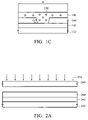
- FIG. 1C is a cross-section of the TFT-LCD shown in FIG. 1B along the plane defined by horizontal dotted line AA′.
- FIGS. 2A to 2C are cross-sections of fabrication of a TFT-LCD according to an embodiment of the present invention.
- FIG. 1A is a top view of a sealant region for a thin film transistor-liquid crystal display (TFT-LCD) according to a comparative example.
- the TFT-LCD apparatus comprises a TFT array substrate 132 , saw tooth openings 134 , a sealant region 136 , and a color filter substrate 140 .
- Sealant 146 shown in FIG. 1C is applied in the openings, forming a sealant region 136 for attachment of the TFT array substrate 132 to the color filter substrate 140 .
- FIG. 1B is a top view of a portion 138 of the sealant region shown in FIG. 1A .
- the width of sealant region 136 is marked by distance m confined by the two vertical lines.
- the width w 1 of the openings equals width w 2 of the openings.
- the sealant 146 shown in FIG. 1C can be evenly distributed on both sides of a central axis S of the sealant region 136 . In other examples, the width w 1 may not equal the width w 2 .
- a fabrication method of the described sealant region pattern comprises the following steps.
- a TFT array substrate 132 is provided.
- a predetermined material layer such as a silicon nitride layer 142 is formed on the TFT array substrate 132 , serving as a passivation layer.
- An organic material layer 144 is formed on the silicon nitride layer 142 .
- the organic material layer 144 is patterned by lithography.
- Saw tooth openings 134 shown in FIG. 1B are formed in the organic material layer 144 by etching, and sealant 146 is placed therein.
- Voids or bubbles 150 formed during application of the sealant 146 occur due to angle ⁇ between sidewall of saw tooth openings 134 and the surface of silicon nitride layer 142 exceeding 60 degrees.
- a method of forming a sealant region pattern for a liquid crystal display is disclosed.
- a TFT array substrate 232 and a color filter substrate 260 opposite thereto are provided.
- a predetermined material layer such as a silicon nitride layer 242 is formed on the TFT array substrate 232 , serving as a passivation layer.
- the passivation layer can comprise silicon oxynitride, silicon oxide, organic dielectric layer, or a combination thereof.
- the predetermined material layer may further comprise Mo, Ti, Al, Ta, metal oxide, metal nitride, or a combination thereof, serving as a metal electrode layer.
- An organic material layer 244 is formed on the silicon nitride layer 242 .
- the organic material layer 244 is patterned by lithography, exposed to UV light 250 through a half-tone mask 248 with a predetermined pattern thereon.
- the predetermined pattern can comprise various openings of different size, providing various local transmittances. Accordingly, the organic material layer 244 is tapered after subsequent development and etching.
- the organic material layer 244 comprises polymethyl methacrylate (PMMA), photosensitive-methylsilsesquiazane (PS-MSZ), or the like.
- saw tooth opening 234 are formed in the organic material layer 244 by etching, similar to saw tooth opening 134 shown in FIG. 1B .
- the half-tone mask 248 can comprise a gray-tone or slit-pattern mask. Preferably, no etching is performed when using photosensitive low-k organic materials in the organic material layer 244 .
- An organic material pattern layer 244 a is formed on the silicon nitride layer 242 after etching. Portions of the silicon nitride layer 242 are exposed by the saw tooth opening 234 in the organic material pattern layer 244 a . Moreover, the sidewall 244 b of saw tooth opening 234 and the surface 242 a of silicon nitride layer 242 form a predetermined angle ⁇ .
- the organic material pattern layer 244 a comprises a plurality of segments 245 adjacent to the saw-tooth opening 234 . The thickness of segments 245 increases with distance from the saw tooth opening.
- the predetermined angle ⁇ is substantially less than 60 degree. In other embodiments, the predetermined angle ⁇ ranges from about 20 degree to about 60 degree, or about 50 degree to about 60 degree, or about 10 degree to about 20 degree, or about 30 degree to about 40 degree, or about 40 degree to about 50 degree, preferably about 20 degree to about 30 degree.
- a predetermined sealant 246 is placed in the saw tooth opening 234 or in the corresponding position of the saw tooth opening 234 of the TFT-LCD substrate 232 for attaching the color filter substrate 260 with the TFT-LCD substrate 232 .
- predetermined angle ⁇ air exhausts easily via the tapered profile of the saw tooth opening 234 during application of sealant, avoiding formation of voids or bubbles in the sealant.
Abstract
Description
Claims (14)
Priority Applications (1)
| Application Number | Priority Date | Filing Date | Title |
|---|---|---|---|
| US11/319,839 US7226801B2 (en) | 2005-01-14 | 2005-12-28 | Sealant region pattern for liquid crystal display and method for fabricating the same |
Applications Claiming Priority (4)
| Application Number | Priority Date | Filing Date | Title |
|---|---|---|---|
| US11/035,647 US7045375B1 (en) | 2005-01-14 | 2005-01-14 | White light emitting device and method of making same |
| TW94121405 | 2005-06-27 | ||
| TW94121405A TWI317035B (en) | 2005-06-27 | 2005-06-27 | A sealant region pattern for a liquid crystal display apparatus and a method for fabricating the same |
| US11/319,839 US7226801B2 (en) | 2005-01-14 | 2005-12-28 | Sealant region pattern for liquid crystal display and method for fabricating the same |
Related Parent Applications (1)
| Application Number | Title | Priority Date | Filing Date |
|---|---|---|---|
| US11/035,647 Continuation-In-Part US7045375B1 (en) | 2005-01-14 | 2005-01-14 | White light emitting device and method of making same |
Publications (2)
| Publication Number | Publication Date |
|---|---|
| US20060160259A1 US20060160259A1 (en) | 2006-07-20 |
| US7226801B2 true US7226801B2 (en) | 2007-06-05 |
Family
ID=36684433
Family Applications (1)
| Application Number | Title | Priority Date | Filing Date |
|---|---|---|---|
| US11/319,839 Active US7226801B2 (en) | 2005-01-14 | 2005-12-28 | Sealant region pattern for liquid crystal display and method for fabricating the same |
Country Status (1)
| Country | Link |
|---|---|
| US (1) | US7226801B2 (en) |
Cited By (1)
| Publication number | Priority date | Publication date | Assignee | Title |
|---|---|---|---|---|
| US9679896B2 (en) * | 2014-12-16 | 2017-06-13 | Samsung Electronics Co., Ltd. | Moisture blocking structure and/or a guard ring, a semiconductor device including the same, and a method of manufacturing the same |
Families Citing this family (4)
| Publication number | Priority date | Publication date | Assignee | Title |
|---|---|---|---|---|
| US8020475B2 (en) * | 2006-06-02 | 2011-09-20 | Kent Displays Incorporated | Method of simultaneous singulation and edge sealing of plastic displays |
| DE102007056924A1 (en) * | 2007-08-31 | 2009-03-05 | Osram Opto Semiconductors Gmbh | Radiation-emitting component i.e. organic LED, has radiation generating layer arranged between electrodes, where one electrode includes structured surfaces comprising regions protruding from surfaces and penetrating into layer |
| CN105549250B (en) * | 2016-02-26 | 2017-11-10 | 京东方科技集团股份有限公司 | A kind of array base palte, display panel and its corresponding preparation method and display device |
| KR102556829B1 (en) * | 2016-06-29 | 2023-07-19 | 삼성디스플레이 주식회사 | Display panel having touch functuion and display apparatus including thereof |
Citations (4)
| Publication number | Priority date | Publication date | Assignee | Title |
|---|---|---|---|---|
| TW464778B (en) | 1995-06-05 | 2001-11-21 | Sampo Corp | Method and device for liquid crystal display |
| US6559917B2 (en) | 2000-11-16 | 2003-05-06 | Nec Corporation | Pattern formation method using reflow enhancement layer and method for manufacturing reflective type liquid crystal display device using the same |
| US20050178498A1 (en) * | 2004-02-18 | 2005-08-18 | Au Optronics Corporation | Method for sealing electroluminescence display devices |
| US6998221B2 (en) * | 2003-05-23 | 2006-02-14 | Texas Instruments Incorporated | Method for forming a via in a substrate |
-
2005
- 2005-12-28 US US11/319,839 patent/US7226801B2/en active Active
Patent Citations (4)
| Publication number | Priority date | Publication date | Assignee | Title |
|---|---|---|---|---|
| TW464778B (en) | 1995-06-05 | 2001-11-21 | Sampo Corp | Method and device for liquid crystal display |
| US6559917B2 (en) | 2000-11-16 | 2003-05-06 | Nec Corporation | Pattern formation method using reflow enhancement layer and method for manufacturing reflective type liquid crystal display device using the same |
| US6998221B2 (en) * | 2003-05-23 | 2006-02-14 | Texas Instruments Incorporated | Method for forming a via in a substrate |
| US20050178498A1 (en) * | 2004-02-18 | 2005-08-18 | Au Optronics Corporation | Method for sealing electroluminescence display devices |
Non-Patent Citations (1)
| Title |
|---|
| Taiwan Office Action mailed May 23, 2006. |
Cited By (1)
| Publication number | Priority date | Publication date | Assignee | Title |
|---|---|---|---|---|
| US9679896B2 (en) * | 2014-12-16 | 2017-06-13 | Samsung Electronics Co., Ltd. | Moisture blocking structure and/or a guard ring, a semiconductor device including the same, and a method of manufacturing the same |
Also Published As
| Publication number | Publication date |
|---|---|
| US20060160259A1 (en) | 2006-07-20 |
Similar Documents
| Publication | Publication Date | Title |
|---|---|---|
| US7884914B2 (en) | Structure for encapsulating a liquid crystal display device | |
| JP5409315B2 (en) | Display device | |
| US7531372B2 (en) | Method for manufacturing array substrate for liquid crystal display device | |
| US7235813B2 (en) | Thin film transistor and pixel structure thereof | |
| US8053295B2 (en) | Liquid crystal display device and method of fabricating the same | |
| US7226801B2 (en) | Sealant region pattern for liquid crystal display and method for fabricating the same | |
| US7477352B2 (en) | Liquid crystal display device including step-compensating pattern and fabricating method thereof | |
| US20090086148A1 (en) | Display Device | |
| KR100872494B1 (en) | manufacturing method of array substrate for liquid crystal display device | |
| TW200423197A (en) | Method for manufacturing optoelectronic device, optoelectronic device and electronic machine | |
| US20060051974A1 (en) | Mask and manufacturing method using mask | |
| US8094251B2 (en) | Method for manufacturing lower substrate of liquid crystal display device | |
| US20100033667A1 (en) | Substrate for liquid crystal display, manufacturing method thereof and panel | |
| US20030017636A1 (en) | Method of fabricating thin film transistor flat panel display | |
| US20090130571A1 (en) | Masking process using photoresist | |
| CN100371806C (en) | Display device sealing region pattern and its forming method | |
| EP1668406B1 (en) | Method of manufacturing liquid crystal display device | |
| JP2007150266A (en) | Solid state imaging device and its manufacturing method | |
| TWI317035B (en) | A sealant region pattern for a liquid crystal display apparatus and a method for fabricating the same | |
| CN101097373A (en) | Mother glass for liquid crystal display and method of fabricating liquid crystal display using the same | |
| KR101268388B1 (en) | Fabrication method of liquid crystal display device | |
| KR101006781B1 (en) | Lcd and method for manufacturing lcd | |
| KR100590919B1 (en) | Method for manufacturing the same | |
| CN117545300A (en) | Display panel and display device | |
| US6914659B2 (en) | Liquid crystal display panel |
Legal Events
| Date | Code | Title | Description |
|---|---|---|---|
| AS | Assignment |
Owner name: AU OPTRONICS CORP., TAIWAN Free format text: ASSIGNMENT OF ASSIGNORS INTEREST;ASSIGNORS:CHIANG, YI-CHEN;HUANG, KUO-YU;REEL/FRAME:017424/0888 Effective date: 20051206 |
|
| STCF | Information on status: patent grant |
Free format text: PATENTED CASE |
|
| FPAY | Fee payment |
Year of fee payment: 4 |
|
| FPAY | Fee payment |
Year of fee payment: 8 |
|
| MAFP | Maintenance fee payment |
Free format text: PAYMENT OF MAINTENANCE FEE, 12TH YEAR, LARGE ENTITY (ORIGINAL EVENT CODE: M1553); ENTITY STATUS OF PATENT OWNER: LARGE ENTITY Year of fee payment: 12 |
|
| AS | Assignment |
Owner name: AUO CORPORATION, TAIWAN Free format text: CHANGE OF NAME;ASSIGNOR:AU OPTRONICS CORPORATION;REEL/FRAME:063785/0830 Effective date: 20220718 |
|
| AS | Assignment |
Owner name: OPTRONIC SCIENCES LLC, TEXAS Free format text: ASSIGNMENT OF ASSIGNORS INTEREST;ASSIGNOR:AUO CORPORATION;REEL/FRAME:064658/0572 Effective date: 20230802 |