US7171499B2 - Processor surrogate for use in multiprocessor systems and multiprocessor system using same - Google Patents
Processor surrogate for use in multiprocessor systems and multiprocessor system using same Download PDFInfo
- Publication number
- US7171499B2 US7171499B2 US10/683,859 US68385903A US7171499B2 US 7171499 B2 US7171499 B2 US 7171499B2 US 68385903 A US68385903 A US 68385903A US 7171499 B2 US7171499 B2 US 7171499B2
- Authority
- US
- United States
- Prior art keywords
- port
- processor
- coupled
- surrogate
- communication link
- Prior art date
- Legal status (The legal status is an assumption and is not a legal conclusion. Google has not performed a legal analysis and makes no representation as to the accuracy of the status listed.)
- Active, expires
Links
Images


Classifications
-
- G—PHYSICS
- G06—COMPUTING; CALCULATING OR COUNTING
- G06F—ELECTRIC DIGITAL DATA PROCESSING
- G06F13/00—Interconnection of, or transfer of information or other signals between, memories, input/output devices or central processing units
- G06F13/38—Information transfer, e.g. on bus
- G06F13/40—Bus structure
- G06F13/4004—Coupling between buses
- G06F13/4027—Coupling between buses using bus bridges
-
- G—PHYSICS
- G06—COMPUTING; CALCULATING OR COUNTING
- G06F—ELECTRIC DIGITAL DATA PROCESSING
- G06F13/00—Interconnection of, or transfer of information or other signals between, memories, input/output devices or central processing units
- G06F13/14—Handling requests for interconnection or transfer
-
- G—PHYSICS
- G06—COMPUTING; CALCULATING OR COUNTING
- G06F—ELECTRIC DIGITAL DATA PROCESSING
- G06F13/00—Interconnection of, or transfer of information or other signals between, memories, input/output devices or central processing units
-
- G—PHYSICS
- G06—COMPUTING; CALCULATING OR COUNTING
- G06F—ELECTRIC DIGITAL DATA PROCESSING
- G06F13/00—Interconnection of, or transfer of information or other signals between, memories, input/output devices or central processing units
- G06F13/38—Information transfer, e.g. on bus
- G06F13/40—Bus structure
Definitions
- the present invention generally relates to data processing systems, and more particularly relates to multiprocessor systems.
- microprocessor speed has created the opportunity for users to upgrade their computer systems with newer, higher speed microprocessors.
- an older, slower microprocessor could be unplugged from its socket and a new, higher speed microprocessor inserted in its place.
- An example of this type of upgradeability is a microprocessor that can communicate with a memory device at one speed but whose internal clock speed can be scaled to a higher frequency, as disclosed in U.S. Pat. No. 5,828,869 to Johnson et al.
- NUMA non-uniform memory accessing
- a processor surrogate is adapted for use in a processing node of a multiprocessor data processing system having a plurality of processing nodes coupled together and to a plurality of input/output devices using corresponding communication links.
- the processor surrogate includes a first port comprising a first set of integrated circuit terminals adapted to be coupled to a first external communication link for coupling to one of the plurality of processing nodes, a second port comprising a second set of integrated circuit terminals adapted to be coupled to a second external communication link for coupling to one of the plurality of input/output devices, and an interconnection circuit coupled between the first port and the second port.
- a multiprocessor data processing system in another form includes first and second processing nodes and an input/output device.
- the first processing node includes an actual processor.
- the second processing node includes a processor surrogate.
- the processor surrogate has a first port coupled to the first processing node, a second port, and an interconnection circuit coupled between the first port and the second port.
- the input/output device is coupled to the second port of the second processing node and is accessible to the actual processor via the processor surrogate.
- FIG. 1 illustrates a block diagram of a multiprocessor computer system useful in understanding the present invention
- FIG. 2 illustrates a block diagram of a portion of the multiprocessor computer system of FIG. 1 including one of the processors and its associated memory;
- FIG. 3 illustrates a block diagram of a multiprocessor computer system using a processor surrogate according to the present invention
- FIG. 4 illustrates in a block diagram of the processor surrogate of FIG. 3 ;
- FIG. 5 illustrates a block diagram of a multiprocessor computer system using a processor surrogate according to another aspect of the present invention
- FIG. 6 illustrates a block diagram of the processor surrogate of FIG. 5 ;
- FIG. 7 illustrates a block diagram of a multiprocessor computer system using the processor surrogate of FIG. 6 according to yet another aspect of the present invention
- FIG. 8 illustrates a top view of an integrated circuit package that may be used for the actual processor of FIG. 2 and the processor surrogates of FIGS. 4 and 6 ;
- FIG. 9 illustrates a side view of the integrated circuit package of FIG. 8 .
- FIG. 10 illustrates a bottom view of the integrated circuit package of FIG. 8 .
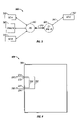
- FIG. 1 illustrates a block diagram of a multiprocessor computer system 100 useful in understanding the present invention.
- Computer system 100 includes two processor nodes represented by circles including a first processor node labeled “P 0 ” and a second processor node labeled “P 1 ” connected together over a communication link 116 .
- Nodes P 0 and P 1 are implemented using microprocessors 110 and 120 , respectively.
- System 100 also includes a first input/output (I/O) device 130 labeled “I/O A”, a second I/O device 140 labeled “I/O B”, a third I/O device 150 labeled “I/O C”, a fourth I/O device 160 labeled “I/O D”, a first dynamic random access memory (DRAM) 170 labeled “DRAM 0 ”, and a second DRAM 180 labeled “DRAM 1 ”.
- Processor 110 is a single-chip microprocessor that communicates with I/O devices 130 and 140 over communication links 112 and 114 , respectively, and with processor 120 over link 116 . Processor 110 also has a dedicated bus for performing memory accesses with local DRAM 170 .
- processor 120 communicates with I/O devices 150 and 160 over corresponding links and has a dedicated bus for connection to local DRAM 180 .
- I/O devices 130 , 140 , 150 , and 160 may be any of a variety of I/O devices including a graphics processor, an Ethernet controller, a bridge to another bus such as that specified by the Personal Computer Interconnect (PCI) Special Interest Group, etc.
- PCI Personal Computer Interconnect
- HyperTransport Technology is a packet-based link implemented on two independent unidirectional sets of wires. So for example links 112 , 114 , and 116 include both an output connection and an input connection. Each HyperTransport link is nominally point-to-point and connects two devices. Chains of HyperTransport links can also be used as an I/O channel, connecting I/O devices and bridges to a host system.
- the HyperTransport link is designed to deliver a high-performance and scalable interconnect between CPU, memory, and I/O devices.
- the HyperTransport link uses low swing differential signaling with on-die differential termination to achieve very high data rates.
- the HyperTransport link uses scalable frequency and data width to achieve scalable bandwidth.
- System 100 includes memory associated with each processor node and distributed among the nodes. It implements a cache coherent non-uniform memory access (“CC NUMA”) architecture.
- CC NUMA cache coherent non-uniform memory access
- the CC NUMA architecture is non-uniform in that all memory in the system is visible to each processor, but access time depends on the physical distance between the processor and the memory.
- processor 110 is able to access DRAM 170 quickly, but must wait while the memory access request travels over link 116 before it can access DRAM 180 .
- Link 116 between processors 110 and 120 uses a special form of HyperTransport known as coherent HyperTransport.
- FIG. 2 illustrates a block diagram of a portion 200 of multiprocessor computer system 100 of FIG. 1 , including processor 110 and DRAM 170 .
- Processor 110 is a single-chip microprocessor and includes generally a central processing unit (CPU) 202 , a memory controller 206 , a crossbar switch labeled “XBAR” 208 , and three link controllers 212 , 214 , and 216 each labeled “HT” for HyperTransport.
- CPU 202 is a processor adapted to execute instructions of the so-called x86 instruction set. The x86 instruction set is based on the instruction set of the 8086 microprocessor first manufactured by the Intel Corporation of Santa Clara, Calif.
- CPU 202 however includes many sophisticated functions for high-performance execution of x86 programs including pipelining and superscalar design.
- CPU 202 includes at least one cache 204 for storage of frequently used data.
- CPU 202 may include two top level (L1) caches, one for instructions and the other one for data, and a second level (L2) cache that is shared by the instruction and data streams.
- Memory controller 206 is the mechanism for data transfer between processor 110 and DRAM 170 .
- Memory controller 206 offloads the task of initiating and terminating memory accesses from CPU 202 . It includes internal queues to allow efficient use of the external bus to DRAM 170 .
- DRAM 170 could be replaced by a lower-level memory system including one or more additional caches and main memory, by static RAM, by nonvolatile memory, etc.
- XBAR 208 is a switching/multiplexing circuit designed to couple together the buses internal to processor 110 .
- Link controllers 212 , 214 , and 216 are coupled to external links 112 , 114 , and 116 , respectively.
- Links 112 , 114 , and 116 include output channels 220 , 230 , and 240 , respectively, and input channels 222 , 232 , and 242 , respectively.
- Each of link controllers 212 , 214 , and 216 comply with the HyperTransportTM I/O Link Specification, Revision 1.05, but additionally support the special coherent form of HyperTransport which is able to link two processor nodes.
- processor 120 is able to access DRAM 170 .
- Processor 120 's own memory controller, corresponding to memory controller 206 , would receive a memory access request from its CPU. Upon recognizing that the access is for memory present at another node, it would send a memory access request to processor 110 through one of its link controllers over coherent link 116 . The request packet would be received by link controller 216 and routed through XBAR 208 to memory controller 206 . Memory controller 206 would then check its internal directory to see whether the requested memory element is present in cache 204 . If the requested memory element were absent from cache 204 , memory controller 206 would read DRAM 170 and provide the requested data element through XBAR 208 and link controller 216 over coherent link 116 back to processor 120 .
- FIG. 3 illustrates a block diagram of a multiprocessor computer system 300 using a processor surrogate 320 according to the present invention.
- multiprocessor means having more than one processing node, even though only one processing node may have an actual CPU.
- System 300 is similar to system 100 except that node P 1 has been replaced by a node labeled “S 1 ” having processor surrogate 320 that does not have its own CPU.
- a “processor surrogate” is a device that plugs into the socket of node S 1 and is used in place of an actual processor.
- System 300 is essentially a single-processor system that may be easily upgraded to a dual processor system. Thus system 300 is a lower cost system but has an upgrade path: an actual processor like that described with respect to FIG. 2 could later be inserted into the socket used by processor surrogate 320 to upgrade significantly the performance of computer system 300 .
- FIG. 4 illustrates a block diagram of processor surrogate 320 of FIG. 3 .
- Processor surrogate 320 is a passive type surrogate and includes a first set of wires 390 to connect input signals of HyperTransport link 370 to output signals of HyperTransport link 380 , and a second set of wires 392 to connect input signals of HyperTransport link 380 to output signals of HyperTransport link 370 .
- Processor surrogate 320 includes integrated circuit terminals, corresponding to terminals of two link controllers of an actual microprocessor, such as microprocessor 110 of FIG. 2 .
- processor 310 On power-up, processor 310 detects whether the HyperTransport link is coherent or non-coherent and negotiates the speed of information transfer over the link. Thus the link controller in processor 310 connected to link 370 will detect, from communication with I/O controller 350 via processor surrogate 320 , that the link is to be non-coherent. However if the processor surrogate were later replaced with an actual processor, then the link controller in processor 310 would detect the presence of an active node and configure it to be a coherent link.
- Processor surrogate 320 has the same “footprint” as processor 110 of FIGS. 1 and 2 , i.e. it is physically capable of plugging or being inserted into a socket that accommodates an actual processor like processor 110 . Thus it would have the same integrated circuit package dimensions as an actual processor. However the integrated circuit package would only contain wires 390 and 392 . In particular one type of package used for processor 110 is a package known as a ceramic micro pin grid array. To accommodate a socket for a micro pin grid array processor, processor surrogate 320 would also use a similar micro pin grid array package. However the pins for most signals would not be connected, and thus would exist as “dummy” pins.
- Pins 372 , 374 , 382 , and 384 would be used to provide the appropriate interconnections.
- a ceramic type package provides the opportunity for forming interconnections using multiple signal planes within the ceramic material to reduce parasitic losses that would otherwise occur through the use of bond wires if a leadframe type package were used.
- Power and ground pins may optionally be connected to provide suitable ground planes for signal shielding from RF radiation and interference.
- processor surrogate 320 may be redesigned to match the footprint of any other package type used for the actual processor. Also it would be possible to substitute a cheaper organic package for the ceramic package if the electrical and mechanical properties were sufficient.
- processor surrogate 320 may be housed in a ceramic micro pin grid array package having a total of 961 available pins formed as an array of 31 rows by 31 columns.
- input ports 372 and 384 each include thirty eight pins, including four clock input pins, two control input pins, and thirty two multiplexed command/address/data input pins, wherein each signal is conducted differentially using a pair of signal pins.
- Output ports 374 and 384 also include thirty eight corresponding pins, including four clock output pins, two control output pins, and thirty two multiplexed command/address/data output pins.
- processor surrogate 320 To make processor surrogate 320 , one would form internal interconnections 390 within the package of processor surrogate 320 by connecting the control input pins of the first link (link 0 ) and the control output pins of the second link (link 1 ), the clock input pins of link 0 and the corresponding clock output pins of link 1 , and the multiplexed command/address/data input pins of link 0 and the corresponding multiplexed command/address/data output pins of link 1 . Similar connections 392 would be made for connecting the inputs of link 1 to the outputs of link 0 .
- a feature of HyperTransport is the ability to scale the number of command/address/data pins from two to thirty-two pairs of pins, and in other embodiments a different number of command/address/data pins besides the sixteen pairs of differential pins described above may be supported.
- FIG. 5 illustrates a block diagram of a multiprocessor computer system 500 using a processor surrogate according to another aspect of the present invention.
- System 500 includes an actual processor 510 in node P 0 and an active form of a processor surrogate 520 in node S 1 .
- Nodes P 0 and S 1 are connected together using a coherent HyperTransport link 590 .
- System 500 includes four I/O devices, including an I/O device 530 labeled “I/O A”, an I/O device 540 labeled “I/O B”, an I/O device 550 labeled “I/O C”, and an I/O device 560 labeled “I/O D”.
- System 500 also includes a first DRAM 570 labeled “DRAM 0 ”, and a second DRAM 580 labeled “DRAM 1 ”, connected respectively to nodes P 0 and S 1 .
- System 500 uses active processor surrogate 520 to allow more resources to be available to node P 0 but without the need for a second actual processor having its own CPU and cache.
- processor surrogate 520 provides interconnection by active circuitry instead of simple wiring to allow processor 510 to access two I/O devices 550 and 560 and an extra DRAM 580 without needing an additional CPU. Since it lacks the CPU and cache, processor surrogate 520 is cheaper than an actual processor but provides an upgrade path for future performance enhancement.
- processor surrogate 520 includes a memory controller 606 , a crossbar switch 608 , and HyperTransport link controllers 612 , 614 , and 616 connected respectively to links 590 , 592 , and 594 .
- HyperTransport link controllers 612 , 614 , and 616 are connected to corresponding ports including sets of output connections 620 , 630 , and 640 and sets of input connections 622 , 632 , and 634 , respectively.
- HyperTransport link controllers 612 , 614 , and 616 are also connected to crossbar switch 608 .
- Memory controller 606 is connected to crossbar switch 608 and to external DRAM 580 .
- crossbar switches 208 and 608 both include a feature to automatically detect the presence or absence of the CPU.
- the design is modular and the integrated circuit used in processor surrogate 520 can be realized by simply deleting the CPU from the netlist and inputting the modified netlist to automated place and route CAD software. Since the CPU consumes a substantial majority of the integrated circuit area of processor 110 , the integrated circuit used in processor surrogate 520 will be significantly less expensive. Alternatively the active processor surrogate could be formed using an actual processor with a defective CPU.
- link 590 uses the coherent form of HyperTransport.
- the link controllers in processor surrogate 520 are modular and are the same as those used in an actual processor. However on power up the link controller in processor surrogate 520 connected to processor 510 over link 590 detects an active device on the other end and configures the link into the coherent form of HyperTransport.
- the protocol is appropriate for a surrogate with its own distributed memory and memory controller.
- FIG. 7 illustrates a block diagram of a multiprocessor computer system 700 using the processor surrogate of FIG. 6 according to yet another aspect of the present invention.
- System 700 illustrates the flexibility of the active form of the processor surrogate in constructing complex system topologies having significant upgrade capabilities.
- System 700 includes four processing nodes labeled “P 0 ”, “S 1 ”, “S 2 ”, and “S 3 ” implemented by an actual processor 710 and processor surrogates 720 , 730 , and 740 , respectively.
- System 700 uses an actual processor such as processor 110 of FIG. 2 for P 0 , and active forms of processor surrogates such as processor surrogate 520 shown in FIG. 6 for nodes S 1 , S 2 , and S 3 .
- the processor nodes are connected in a ring using coherent HyperTransport links such that node P 0 is connected to adjacent nodes S 1 and S 3 , node S 1 is connected to adjacent nodes P 0 and S 2 , node S 2 is connected to adjacent nodes S 1 and S 3 , and node S 3 is connected to adjacent nodes S 2 and P 0 .
- System 700 provides accessibility to DRAM and I/O devices connected to three active processor surrogates but without the need for additional CPUs required by actual processors. It also provides a significant upgrade path in the ability to expand the system to up to four processors.
- processor node topologies may be used and all such multiprocessor topologies may be populated with at least one actual processor and one or more processor surrogates to provide flexible upgrade paths.
- processor 110 of FIG. 2 supports communication over three HyperTransport links using three corresponding link controllers
- an actual processor may include a different number of link controllers and the possibilities for use of processor surrogates vary as well.
- processor surrogates vary as well.
- actual processor 110 included four link controllers a passive form of the processor surrogate could allow connection of processor 110 to two extra I/O devices connected to the processor surrogate in a two-node multiprocessor system.
- the availability of four link controllers also allows more complex network topologies that those specifically illustrated herein.
- processor surrogate and multiprocessor systems were described herein in the context of a HyperTransport NUMA architecture.
- other inter-processor communication protocols may also be used.
- inter-processor communication protocol need not be implemented using coherent links.
- software coherence management could be used with non-coherent inter-processor communication links.
- the disclosed microprocessor may implement other instruction sets than the x86 instruction set.
- FIG. 8 illustrates a top view 800 of an integrated circuit package that may be used for actual processor 110 of FIG. 2 and for processor surrogate 320 of FIG. 4 and processor surrogate 520 of FIG. 6 .
- the exemplary integrated circuit package is a micro pin grid array package.
- the pin grid array package is a package type that is especially well suited for replacement because it can be matched with a corresponding socket, and the processor surrogate can be easily extracted from it and replaced with an actual processor.
- From top view 800 it can be seen that the micro pin grid array package has a base portion 802 and a lid portion 804 within a central portion of the area defined by base portion 802 .
- Base portion 802 has a bevel 806 in the upper right corner signifying the “A 1 ” corner, as will be described more fully below.
- FIG. 9 illustrates a side view 900 of the integrated circuit package of FIG. 8 .
- base portion 902 and lid 904 From side view 900 is seen base portion 902 and lid 904 .
- Beneath base portion 902 is a plurality of integrated circuit terminals in the form of an array of pins 906 extending downward from the bottom surface of base 902 .
- FIG. 10 illustrates a bottom view 1000 of the integrated circuit package of FIG. 8 .
- A1 corner 1002 and an array of pins extending toward the viewer represented by solid circles.
- the package outlines a possible array of pins formed by columns 1004 and rows 1006 .
- Rows 1004 include 31 rows and columns 1006 include 31 columns for a potential array of 961 pins. However, pins are not present in the corners and in several areas within the array so that the total number of pins is equal to 940.
- the rows are assigned letters in the sequence A, B, C . . . H, J . . . M, N, P, R, S . . . V, W, Y, AA, AB . . . AH, AJ, AK, AL from top to bottom and the columns are numbered from 1 to 31 from right to left.
- a normal processor has a pin assignment including the following pertinent pin assignments shown in TABLE I for link controller 212 and in TABLE II for link controller 214 :
- pin L 0 _CADIN_L[ 0 ] (assigned to pin location G 2 ) would be connected to pin L 1 _CADOUT_L[ 0 ] (assigned to pin location A 4 )
- pin L 1 _CADIN_H[ 15 ] (assigned to pin location E 14 ) would be connected to pin L 0 _CADOUT_H[ 15 ] (assigned to pin location V 4 ), and so on.
Landscapes
- Engineering & Computer Science (AREA)
- Theoretical Computer Science (AREA)
- General Engineering & Computer Science (AREA)
- Physics & Mathematics (AREA)
- General Physics & Mathematics (AREA)
- Computer Hardware Design (AREA)
- Multi Processors (AREA)
Priority Applications (8)
| Application Number | Priority Date | Filing Date | Title |
|---|---|---|---|
| US10/683,859 US7171499B2 (en) | 2003-10-10 | 2003-10-10 | Processor surrogate for use in multiprocessor systems and multiprocessor system using same |
| EP04754332A EP1671238B1 (en) | 2003-10-10 | 2004-06-04 | Processor surrogate for use in multiprocessor systems and multiprocessor system using same |
| KR1020067009129A KR101077285B1 (ko) | 2003-10-10 | 2004-06-04 | 멀티프로세서 시스템들에서 사용하기 위한 프로세서써로게이트와 이를 사용하는 멀티프로세서 시스템 |
| CN2004800367208A CN1890653B (zh) | 2003-10-10 | 2004-06-04 | 用于多处理器系统中的处理器代用品以及使用该处理器代用品的多处理器系统 |
| PCT/US2004/017704 WO2005041053A2 (en) | 2003-10-10 | 2004-06-04 | Processor surrogate for use in multiprocessor systems and multiprocessor system using same |
| DE602004014169T DE602004014169D1 (de) | 2003-10-10 | 2004-06-04 | Prozessor-surrogat zur verwendung in mehrprozessor-systemen und mehrprozessor-system damit |
| GB0607619A GB2423170B (en) | 2003-10-10 | 2004-06-04 | Processor surrogate for use in multiprocessor systems and multiprocessor system using same |
| TW093129816A TWI353523B (en) | 2003-10-10 | 2004-10-01 | Processor surrogate for use in multiprocessor syst |
Applications Claiming Priority (1)
| Application Number | Priority Date | Filing Date | Title |
|---|---|---|---|
| US10/683,859 US7171499B2 (en) | 2003-10-10 | 2003-10-10 | Processor surrogate for use in multiprocessor systems and multiprocessor system using same |
Publications (2)
| Publication Number | Publication Date |
|---|---|
| US20050080978A1 US20050080978A1 (en) | 2005-04-14 |
| US7171499B2 true US7171499B2 (en) | 2007-01-30 |
Family
ID=34422850
Family Applications (1)
| Application Number | Title | Priority Date | Filing Date |
|---|---|---|---|
| US10/683,859 Active 2024-10-15 US7171499B2 (en) | 2003-10-10 | 2003-10-10 | Processor surrogate for use in multiprocessor systems and multiprocessor system using same |
Country Status (8)
| Country | Link |
|---|---|
| US (1) | US7171499B2 (ko) |
| EP (1) | EP1671238B1 (ko) |
| KR (1) | KR101077285B1 (ko) |
| CN (1) | CN1890653B (ko) |
| DE (1) | DE602004014169D1 (ko) |
| GB (1) | GB2423170B (ko) |
| TW (1) | TWI353523B (ko) |
| WO (1) | WO2005041053A2 (ko) |
Cited By (9)
| Publication number | Priority date | Publication date | Assignee | Title |
|---|---|---|---|---|
| US20060095593A1 (en) * | 2004-10-29 | 2006-05-04 | Advanced Micro Devices, Inc. | Parallel processing mechanism for multi-processor systems |
| US20070106831A1 (en) * | 2005-11-09 | 2007-05-10 | Shan-Kai Yang | Computer system and bridge module thereof |
| US20070143520A1 (en) * | 2005-12-16 | 2007-06-21 | Shan-Kai Yang | Bridge, computer system and method for initialization |
| US20070162678A1 (en) * | 2006-01-06 | 2007-07-12 | Shan-Kai Yang | Computer system and memory bridge for processor socket thereof |
| US20080114918A1 (en) * | 2006-11-09 | 2008-05-15 | Advanced Micro Devices, Inc. | Configurable computer system |
| US20080184021A1 (en) * | 2007-01-26 | 2008-07-31 | Wilson Lee H | Flexibly configurable multi central processing unit (cpu) supported hypertransport switching |
| US20080256222A1 (en) * | 2007-01-26 | 2008-10-16 | Wilson Lee H | Structure for a flexibly configurable multi central processing unit (cpu) supported hypertransport switching |
| US20100002099A1 (en) * | 2006-07-28 | 2010-01-07 | Mtekvision Co., Ltd. | Method and apparatus for sharing memory |
| US20120260016A1 (en) * | 2011-04-06 | 2012-10-11 | International Business Machines Corporation | Multi-use physical architecture |
Families Citing this family (8)
| Publication number | Priority date | Publication date | Assignee | Title |
|---|---|---|---|---|
| US6836815B1 (en) * | 2001-07-11 | 2004-12-28 | Pasternak Solutions Llc | Layered crossbar for interconnection of multiple processors and shared memories |
| JP4895972B2 (ja) * | 2007-10-22 | 2012-03-14 | アラクサラネットワークス株式会社 | リングプロトコル高速切替方法およびその装置 |
| US8732331B2 (en) * | 2008-10-02 | 2014-05-20 | Hewlett-Packard Development Company, L.P. | Managing latencies in a multiprocessor interconnect |
| US8373709B2 (en) * | 2008-10-03 | 2013-02-12 | Ati Technologies Ulc | Multi-processor architecture and method |
| US7741867B2 (en) * | 2008-10-30 | 2010-06-22 | Hewlett-Packard Development Company, L.P. | Differential on-line termination |
| US9678159B2 (en) * | 2015-03-04 | 2017-06-13 | Cavium, Inc. | Communication and control topology for efficient testing of sets of devices |
| US10268630B1 (en) * | 2017-10-24 | 2019-04-23 | Hewlett Packard Enterprise Development Lp | Noncoherent interprocessor communication remapping node controller |
| US10360167B1 (en) * | 2018-01-22 | 2019-07-23 | Dell Products L.P. | Systems and methods for using a bus exchange switch to control processor affinity |
Citations (19)
| Publication number | Priority date | Publication date | Assignee | Title |
|---|---|---|---|---|
| US4014005A (en) | 1976-01-05 | 1977-03-22 | International Business Machines Corporation | Configuration and control unit for a heterogeneous multi-system |
| US5297272A (en) | 1989-08-02 | 1994-03-22 | Advanced Logic Research, Inc. | Apparatus for automatically disabling and isolating a computer's original processor upon installation of a processor upgrade card |
| US5455927A (en) | 1991-08-22 | 1995-10-03 | Acer Incorporated | Dual socket upgradeable computer motherboard with automatic detection and enablement of inserted upgrade CPU chip |
| US5828869A (en) | 1991-03-01 | 1998-10-27 | Advanced Micro Devices, Inc. | Microprocessor arranged for synchronously accessing an external memory with a scalable clocking mechanism |
| US6128685A (en) * | 1998-02-18 | 2000-10-03 | Micron Technology, Inc. | Method for terminating a processor bus |
| US20020087807A1 (en) * | 2000-06-10 | 2002-07-04 | Kourosh Gharachorloo | System for minimizing directory information in scalable multiprocessor systems with logically independent input/output nodes |
| US6553430B1 (en) * | 1999-09-17 | 2003-04-22 | Advanced Micro Devices, Inc. | Computer system implementing flush operation |
| US6626690B2 (en) * | 2001-08-01 | 2003-09-30 | Hewlett-Packard Development Company, L.P. | Low profile NIC jumper solution using ZIF connector |
| US6633960B1 (en) * | 2000-08-31 | 2003-10-14 | Hewlett-Packard Development Company, L.P. | Scalable directory based cache coherence protocol |
| US6651131B1 (en) * | 2000-09-06 | 2003-11-18 | Sun Microsystems, Inc. | High bandwidth network and storage card |
| US6675265B2 (en) * | 2000-06-10 | 2004-01-06 | Hewlett-Packard Development Company, L.P. | Multiprocessor cache coherence system and method in which processor nodes and input/output nodes are equal participants |
| US20040093404A1 (en) * | 2000-04-29 | 2004-05-13 | Snyder Robert D. | Protocol for identifying components in a point-to-point computer system |
| US20040236891A1 (en) * | 2003-04-28 | 2004-11-25 | International Business Machines Corporation | Processor book for building large scalable processor systems |
| US20040268000A1 (en) * | 2003-06-24 | 2004-12-30 | Barker John Howard | Pass through circuit for reduced memory latency in a multiprocessor system |
| US20050053057A1 (en) * | 1999-09-29 | 2005-03-10 | Silicon Graphics, Inc. | Multiprocessor node controller circuit and method |
| US6874070B2 (en) * | 2002-02-22 | 2005-03-29 | Hewlett-Packard Development Company, L.P. | System and method for memory interleaving using cell map with entry grouping for higher-way interleaving |
| US6944719B2 (en) * | 2002-05-15 | 2005-09-13 | Broadcom Corp. | Scalable cache coherent distributed shared memory processing system |
| US20050243531A1 (en) * | 2004-04-29 | 2005-11-03 | Newisys, Inc., A Delaware Corporation | Interposer device |
| US20060080484A1 (en) * | 2004-10-07 | 2006-04-13 | Lefebvre Joel P | System having a module adapted to be included in the system in place of a processor |
Family Cites Families (1)
| Publication number | Priority date | Publication date | Assignee | Title |
|---|---|---|---|---|
| US6877061B2 (en) * | 2000-03-31 | 2005-04-05 | Emc Corporation | Data storage system having dummy printed circuit boards |
-
2003
- 2003-10-10 US US10/683,859 patent/US7171499B2/en active Active
-
2004
- 2004-06-04 KR KR1020067009129A patent/KR101077285B1/ko not_active IP Right Cessation
- 2004-06-04 CN CN2004800367208A patent/CN1890653B/zh active Active
- 2004-06-04 DE DE602004014169T patent/DE602004014169D1/de active Active
- 2004-06-04 GB GB0607619A patent/GB2423170B/en active Active
- 2004-06-04 WO PCT/US2004/017704 patent/WO2005041053A2/en active Search and Examination
- 2004-06-04 EP EP04754332A patent/EP1671238B1/en active Active
- 2004-10-01 TW TW093129816A patent/TWI353523B/zh active
Patent Citations (21)
| Publication number | Priority date | Publication date | Assignee | Title |
|---|---|---|---|---|
| US4014005A (en) | 1976-01-05 | 1977-03-22 | International Business Machines Corporation | Configuration and control unit for a heterogeneous multi-system |
| US5297272A (en) | 1989-08-02 | 1994-03-22 | Advanced Logic Research, Inc. | Apparatus for automatically disabling and isolating a computer's original processor upon installation of a processor upgrade card |
| US5828869A (en) | 1991-03-01 | 1998-10-27 | Advanced Micro Devices, Inc. | Microprocessor arranged for synchronously accessing an external memory with a scalable clocking mechanism |
| US5455927A (en) | 1991-08-22 | 1995-10-03 | Acer Incorporated | Dual socket upgradeable computer motherboard with automatic detection and enablement of inserted upgrade CPU chip |
| US6128685A (en) * | 1998-02-18 | 2000-10-03 | Micron Technology, Inc. | Method for terminating a processor bus |
| US6553430B1 (en) * | 1999-09-17 | 2003-04-22 | Advanced Micro Devices, Inc. | Computer system implementing flush operation |
| US20050053057A1 (en) * | 1999-09-29 | 2005-03-10 | Silicon Graphics, Inc. | Multiprocessor node controller circuit and method |
| US20040093404A1 (en) * | 2000-04-29 | 2004-05-13 | Snyder Robert D. | Protocol for identifying components in a point-to-point computer system |
| US20020087807A1 (en) * | 2000-06-10 | 2002-07-04 | Kourosh Gharachorloo | System for minimizing directory information in scalable multiprocessor systems with logically independent input/output nodes |
| US6675265B2 (en) * | 2000-06-10 | 2004-01-06 | Hewlett-Packard Development Company, L.P. | Multiprocessor cache coherence system and method in which processor nodes and input/output nodes are equal participants |
| US6633960B1 (en) * | 2000-08-31 | 2003-10-14 | Hewlett-Packard Development Company, L.P. | Scalable directory based cache coherence protocol |
| US6651131B1 (en) * | 2000-09-06 | 2003-11-18 | Sun Microsystems, Inc. | High bandwidth network and storage card |
| US6766577B2 (en) * | 2001-08-01 | 2004-07-27 | Hewlett-Packard Development Company, L.P. | Method for changeably connecting electronic devices |
| US6626690B2 (en) * | 2001-08-01 | 2003-09-30 | Hewlett-Packard Development Company, L.P. | Low profile NIC jumper solution using ZIF connector |
| US6874070B2 (en) * | 2002-02-22 | 2005-03-29 | Hewlett-Packard Development Company, L.P. | System and method for memory interleaving using cell map with entry grouping for higher-way interleaving |
| US6944719B2 (en) * | 2002-05-15 | 2005-09-13 | Broadcom Corp. | Scalable cache coherent distributed shared memory processing system |
| US20040236891A1 (en) * | 2003-04-28 | 2004-11-25 | International Business Machines Corporation | Processor book for building large scalable processor systems |
| US20040268000A1 (en) * | 2003-06-24 | 2004-12-30 | Barker John Howard | Pass through circuit for reduced memory latency in a multiprocessor system |
| US7007125B2 (en) * | 2003-06-24 | 2006-02-28 | International Business Machines Corporation | Pass through circuit for reduced memory latency in a multiprocessor system |
| US20050243531A1 (en) * | 2004-04-29 | 2005-11-03 | Newisys, Inc., A Delaware Corporation | Interposer device |
| US20060080484A1 (en) * | 2004-10-07 | 2006-04-13 | Lefebvre Joel P | System having a module adapted to be included in the system in place of a processor |
Non-Patent Citations (2)
| Title |
|---|
| "The AMD Opteron Processor for Multiprocessor Servers," Chetana N. Keltcher et al., IEEE, 2003, pp. 66-76. |
| HyperTransport(TM) I/O Link Specification, Revision 1.05, (C) 2003 HyperTransport Technology Consortium. |
Cited By (13)
| Publication number | Priority date | Publication date | Assignee | Title |
|---|---|---|---|---|
| US20060095593A1 (en) * | 2004-10-29 | 2006-05-04 | Advanced Micro Devices, Inc. | Parallel processing mechanism for multi-processor systems |
| US20070106831A1 (en) * | 2005-11-09 | 2007-05-10 | Shan-Kai Yang | Computer system and bridge module thereof |
| US20070143520A1 (en) * | 2005-12-16 | 2007-06-21 | Shan-Kai Yang | Bridge, computer system and method for initialization |
| US7512731B2 (en) * | 2006-01-06 | 2009-03-31 | Mitac International Corp. | Computer system and memory bridge for processor socket thereof |
| US20070162678A1 (en) * | 2006-01-06 | 2007-07-12 | Shan-Kai Yang | Computer system and memory bridge for processor socket thereof |
| US20100002099A1 (en) * | 2006-07-28 | 2010-01-07 | Mtekvision Co., Ltd. | Method and apparatus for sharing memory |
| US20080114918A1 (en) * | 2006-11-09 | 2008-05-15 | Advanced Micro Devices, Inc. | Configurable computer system |
| US20080256222A1 (en) * | 2007-01-26 | 2008-10-16 | Wilson Lee H | Structure for a flexibly configurable multi central processing unit (cpu) supported hypertransport switching |
| US20080184021A1 (en) * | 2007-01-26 | 2008-07-31 | Wilson Lee H | Flexibly configurable multi central processing unit (cpu) supported hypertransport switching |
| US7797475B2 (en) * | 2007-01-26 | 2010-09-14 | International Business Machines Corporation | Flexibly configurable multi central processing unit (CPU) supported hypertransport switching |
| US7853638B2 (en) | 2007-01-26 | 2010-12-14 | International Business Machines Corporation | Structure for a flexibly configurable multi central processing unit (CPU) supported hypertransport switching |
| US20120260016A1 (en) * | 2011-04-06 | 2012-10-11 | International Business Machines Corporation | Multi-use physical architecture |
| US8543753B2 (en) * | 2011-04-06 | 2013-09-24 | International Business Machines Corporation | Multi-use physical architecture |
Also Published As
| Publication number | Publication date |
|---|---|
| US20050080978A1 (en) | 2005-04-14 |
| GB2423170A (en) | 2006-08-16 |
| GB0607619D0 (en) | 2006-05-31 |
| KR20060111505A (ko) | 2006-10-27 |
| DE602004014169D1 (de) | 2008-07-10 |
| KR101077285B1 (ko) | 2011-10-27 |
| TWI353523B (en) | 2011-12-01 |
| WO2005041053A2 (en) | 2005-05-06 |
| WO2005041053A3 (en) | 2005-11-03 |
| CN1890653A (zh) | 2007-01-03 |
| GB2423170B (en) | 2007-06-06 |
| TW200519617A (en) | 2005-06-16 |
| EP1671238A2 (en) | 2006-06-21 |
| EP1671238B1 (en) | 2008-05-28 |
| CN1890653B (zh) | 2010-06-23 |
Similar Documents
| Publication | Publication Date | Title |
|---|---|---|
| US7171499B2 (en) | Processor surrogate for use in multiprocessor systems and multiprocessor system using same | |
| US11080449B2 (en) | Modular periphery tile for integrated circuit device | |
| US9940279B2 (en) | Processor apparatus with programmable multi port serial communication interconnections | |
| US20180210852A1 (en) | Scalable multi-core system-on-chip architecture on multiple dice for high end microcontroller | |
| KR100690557B1 (ko) | 시스템 온 칩 디자인을 위한 컴포넌트로서의 독립프로세서 서브시스템 | |
| US20040236891A1 (en) | Processor book for building large scalable processor systems | |
| US9886275B1 (en) | Multi-core processor using three dimensional integration | |
| US7213224B2 (en) | Customizable development and demonstration platform for structured ASICs | |
| US20230378061A1 (en) | Fabric Die to Fabric Die Interconnect for Modularized Integrated Circuit Devices | |
| US20130247038A1 (en) | Device-integration method, terminal-apparatus, and distributed multi-terminal-apparatus system | |
| NO343359B1 (en) | Interconnect switch in multiprocessor systems | |
| US20050193178A1 (en) | Systems and methods for flexible extension of SAS expander ports | |
| US20040022022A1 (en) | Modular system customized by system backplane | |
| US8782302B2 (en) | Method and apparatus for routing transactions through partitions of a system-on-chip | |
| TWI771952B (zh) | 利用基板管理控制器進行韌體更新動作的伺服器系統 | |
| CN114063725B (zh) | 用于计算和存储集群的模块化基础设施 | |
| US20230325345A1 (en) | Mesh network-on-a-chip (noc) with heterogeneous routers | |
| KR20230073254A (ko) | Pcie 디바이스를 위한 가상 핫 플러그 시스템 및 방법 | |
| JP2001127166A (ja) | 集積回路の製造方法 | |
| JPH03195044A (ja) | 半導体集積回路及び半導体集積回路の開発方法 |
Legal Events
| Date | Code | Title | Description |
|---|---|---|---|
| AS | Assignment |
Owner name: ADVANCED MICRO DEVICES, TEXAS Free format text: ASSIGNMENT OF ASSIGNORS INTEREST;ASSIGNORS:KELLEY, BRENT;BRANTLEY, WILLIAM C.;REEL/FRAME:014689/0337 Effective date: 20031008 |
|
| FEPP | Fee payment procedure |
Free format text: PAYOR NUMBER ASSIGNED (ORIGINAL EVENT CODE: ASPN); ENTITY STATUS OF PATENT OWNER: LARGE ENTITY |
|
| STCF | Information on status: patent grant |
Free format text: PATENTED CASE |
|
| FPAY | Fee payment |
Year of fee payment: 4 |
|
| FPAY | Fee payment |
Year of fee payment: 8 |
|
| MAFP | Maintenance fee payment |
Free format text: PAYMENT OF MAINTENANCE FEE, 12TH YEAR, LARGE ENTITY (ORIGINAL EVENT CODE: M1553) Year of fee payment: 12 |