US7166859B2 - Organic semiconductor transistor element, semiconductor device using the same, and process for producing the semiconductor device - Google Patents

Organic semiconductor transistor element, semiconductor device using the same, and process for producing the semiconductor device Download PDF

Info

Publication number
US7166859B2
US7166859B2 US10/959,224 US95922404A US7166859B2 US 7166859 B2 US7166859 B2 US 7166859B2 US 95922404 A US95922404 A US 95922404A US 7166859 B2 US7166859 B2 US 7166859B2
Authority
US
United States
Prior art keywords
organic semiconductor
aromatic
substituted
bivalent
polymer compound
Prior art date
Legal status (The legal status is an assumption and is not a legal conclusion. Google has not performed a legal analysis and makes no representation as to the accuracy of the status listed.)
Expired - Fee Related, expires
Application number
US10/959,224
Other versions
US20050104097A1 (en
Inventor
Hidekazu Hirose
Mieko Seki
Daisuke Okuda
Tadayoshi Ozaki
Takeshi Agata
Toru Ishii
Kiyokazu Mashimo
Katsuhiro Sato
Hiroaki Moriyama
Yohei Nishino
Current Assignee (The listed assignees may be inaccurate. Google has not performed a legal analysis and makes no representation or warranty as to the accuracy of the list.)
Fujifilm Business Innovation Corp
Original Assignee
Fuji Xerox Co Ltd
Priority date (The priority date is an assumption and is not a legal conclusion. Google has not performed a legal analysis and makes no representation as to the accuracy of the date listed.)
Filing date
Publication date
Application filed by Fuji Xerox Co Ltd filed Critical Fuji Xerox Co Ltd
Assigned to FUJI XEROX CO., LTD. reassignment FUJI XEROX CO., LTD. ASSIGNMENT OF ASSIGNORS INTEREST (SEE DOCUMENT FOR DETAILS). Assignors: AGATA, TAKESHI, HIROSE, HIDEKAZU, ISHII, TORU, MASHIMO, KIYOKAZU, MORIYAMA, HIROAKI, NISHINO, YOHEI, OKUDA, DAISUKE, OZAKI, TADAYOSHI, SATO, KATSUHIRO, SEKI, MIEKO
Publication of US20050104097A1 publication Critical patent/US20050104097A1/en
Application granted granted Critical
Publication of US7166859B2 publication Critical patent/US7166859B2/en
Expired - Fee Related legal-status Critical Current
Adjusted expiration legal-status Critical

Links

Images

Classifications

    • HELECTRICITY
    • H10SEMICONDUCTOR DEVICES; ELECTRIC SOLID-STATE DEVICES NOT OTHERWISE PROVIDED FOR
    • H10KORGANIC ELECTRIC SOLID-STATE DEVICES
    • H10K85/00Organic materials used in the body or electrodes of devices covered by this subclass
    • H10K85/10Organic polymers or oligomers
    • H10K85/111Organic polymers or oligomers comprising aromatic, heteroaromatic, or aryl chains, e.g. polyaniline, polyphenylene or polyphenylene vinylene
    • HELECTRICITY
    • H01ELECTRIC ELEMENTS
    • H01LSEMICONDUCTOR DEVICES NOT COVERED BY CLASS H10
    • H01L21/00Processes or apparatus adapted for the manufacture or treatment of semiconductor or solid state devices or of parts thereof
    • H01L21/02Manufacture or treatment of semiconductor devices or of parts thereof
    • H01L21/04Manufacture or treatment of semiconductor devices or of parts thereof the devices having at least one potential-jump barrier or surface barrier, e.g. PN junction, depletion layer or carrier concentration layer
    • H01L21/18Manufacture or treatment of semiconductor devices or of parts thereof the devices having at least one potential-jump barrier or surface barrier, e.g. PN junction, depletion layer or carrier concentration layer the devices having semiconductor bodies comprising elements of Group IV of the Periodic System or AIIIBV compounds with or without impurities, e.g. doping materials
    • GPHYSICS
    • G02OPTICS
    • G02FOPTICAL DEVICES OR ARRANGEMENTS FOR THE CONTROL OF LIGHT BY MODIFICATION OF THE OPTICAL PROPERTIES OF THE MEDIA OF THE ELEMENTS INVOLVED THEREIN; NON-LINEAR OPTICS; FREQUENCY-CHANGING OF LIGHT; OPTICAL LOGIC ELEMENTS; OPTICAL ANALOGUE/DIGITAL CONVERTERS
    • G02F1/00Devices or arrangements for the control of the intensity, colour, phase, polarisation or direction of light arriving from an independent light source, e.g. switching, gating or modulating; Non-linear optics
    • G02F1/01Devices or arrangements for the control of the intensity, colour, phase, polarisation or direction of light arriving from an independent light source, e.g. switching, gating or modulating; Non-linear optics for the control of the intensity, phase, polarisation or colour 
    • G02F1/15Devices or arrangements for the control of the intensity, colour, phase, polarisation or direction of light arriving from an independent light source, e.g. switching, gating or modulating; Non-linear optics for the control of the intensity, phase, polarisation or colour  based on an electrochromic effect
    • G02F1/153Constructional details
    • HELECTRICITY
    • H10SEMICONDUCTOR DEVICES; ELECTRIC SOLID-STATE DEVICES NOT OTHERWISE PROVIDED FOR
    • H10KORGANIC ELECTRIC SOLID-STATE DEVICES
    • H10K10/00Organic devices specially adapted for rectifying, amplifying, oscillating or switching; Organic capacitors or resistors having a potential-jump barrier or a surface barrier
    • H10K10/40Organic transistors
    • H10K10/46Field-effect transistors, e.g. organic thin-film transistors [OTFT]
    • H10K10/462Insulated gate field-effect transistors [IGFETs]
    • H10K10/466Lateral bottom-gate IGFETs comprising only a single gate
    • HELECTRICITY
    • H10SEMICONDUCTOR DEVICES; ELECTRIC SOLID-STATE DEVICES NOT OTHERWISE PROVIDED FOR
    • H10KORGANIC ELECTRIC SOLID-STATE DEVICES
    • H10K85/00Organic materials used in the body or electrodes of devices covered by this subclass
    • H10K85/60Organic compounds having low molecular weight
    • H10K85/631Amine compounds having at least two aryl rest on at least one amine-nitrogen atom, e.g. triphenylamine
    • HELECTRICITY
    • H10SEMICONDUCTOR DEVICES; ELECTRIC SOLID-STATE DEVICES NOT OTHERWISE PROVIDED FOR
    • H10KORGANIC ELECTRIC SOLID-STATE DEVICES
    • H10K10/00Organic devices specially adapted for rectifying, amplifying, oscillating or switching; Organic capacitors or resistors having a potential-jump barrier or a surface barrier
    • H10K10/40Organic transistors
    • H10K10/46Field-effect transistors, e.g. organic thin-film transistors [OTFT]
    • H10K10/462Insulated gate field-effect transistors [IGFETs]
    • H10K10/491Vertical transistors, e.g. vertical carbon nanotube field effect transistors [CNT-FETs]
    • HELECTRICITY
    • H10SEMICONDUCTOR DEVICES; ELECTRIC SOLID-STATE DEVICES NOT OTHERWISE PROVIDED FOR
    • H10KORGANIC ELECTRIC SOLID-STATE DEVICES
    • H10K85/00Organic materials used in the body or electrodes of devices covered by this subclass
    • H10K85/10Organic polymers or oligomers
    • H10K85/111Organic polymers or oligomers comprising aromatic, heteroaromatic, or aryl chains, e.g. polyaniline, polyphenylene or polyphenylene vinylene
    • H10K85/113Heteroaromatic compounds comprising sulfur or selene, e.g. polythiophene
    • HELECTRICITY
    • H10SEMICONDUCTOR DEVICES; ELECTRIC SOLID-STATE DEVICES NOT OTHERWISE PROVIDED FOR
    • H10KORGANIC ELECTRIC SOLID-STATE DEVICES
    • H10K85/00Organic materials used in the body or electrodes of devices covered by this subclass
    • H10K85/10Organic polymers or oligomers
    • H10K85/151Copolymers
    • HELECTRICITY
    • H10SEMICONDUCTOR DEVICES; ELECTRIC SOLID-STATE DEVICES NOT OTHERWISE PROVIDED FOR
    • H10KORGANIC ELECTRIC SOLID-STATE DEVICES
    • H10K85/00Organic materials used in the body or electrodes of devices covered by this subclass
    • H10K85/60Organic compounds having low molecular weight
    • H10K85/615Polycyclic condensed aromatic hydrocarbons, e.g. anthracene
    • HELECTRICITY
    • H10SEMICONDUCTOR DEVICES; ELECTRIC SOLID-STATE DEVICES NOT OTHERWISE PROVIDED FOR
    • H10KORGANIC ELECTRIC SOLID-STATE DEVICES
    • H10K85/00Organic materials used in the body or electrodes of devices covered by this subclass
    • H10K85/60Organic compounds having low molecular weight
    • H10K85/649Aromatic compounds comprising a hetero atom
    • H10K85/656Aromatic compounds comprising a hetero atom comprising two or more different heteroatoms per ring
    • H10K85/6565Oxadiazole compounds

Definitions

  • the present invention relates to an organic semiconductor transistor element using an organic semiconductor, a semiconductor device using this element, and a process for producing the semiconductor. More specifically, the present invention relates to an organic semiconductor transistor element which can be used suitably in the fields of driving circuits of display elements (such as electronic paper, digital paper, organic EL elements, electrophoresis type display elements or liquid crystal elements), logic circuits or memory elements used in electronic tags, smart cards or the like, gas sensors or the like, semiconductor devices using this element, and also relates to a process for producing the semiconductor device.
  • display elements such as electronic paper, digital paper, organic EL elements, electrophoresis type display elements or liquid crystal elements
  • logic circuits or memory elements used in electronic tags, smart cards or the like, gas sensors or the like
  • semiconductor devices using this element and also relates to a process for producing the semiconductor device.
  • Thin film transistors are widely used as switching elements for displays, for example, as liquid crystal display elements.
  • thin film transistors have been produced from amorphous or polycrystal silicon.
  • the production of thin film transistors from silicon involves production process using a vacuum system such as sputtering or CVD equipment, and involves a very high cost.
  • a vacuum system such as sputtering or CVD equipment
  • the process for forming a film from amorphous or polycrystal silicon is performed at a very high temperature.
  • material which can be used as a substrate for the film is limited. Consequently, the problem remains of an inability to use a light and flexible substrate, such as a resin substrate.
  • Organic semiconductors a typical example of which is an organic EL element, have also undergone active research in recent years. In tandem with this, there have also been studies of integrating organic material into a circuit, the organic material having characteristics of lightness and flexibility that silicon material does not have.
  • a low molecular weight compound or a polymer compound is adopted for the organic material used in this kind of thin film transistor.
  • polyacene compounds such as pentacene and tetracene (see, for example, Japanese Patent Application Laid-Open (JP-A-) Nos. 5-55568, 10-270712 and 2001-94107) and phthalocyanine compounds such as copper phthalocyanine are suggested (see, for example, JP-A Nos. 5-190877 and 2000-174277).
  • aromatic oligomers such as sexithiophene (see, for example, JP-A No. 8-264805), and polymer compounds such as polythiophene, polythienylvinylene, and poly(p-phenylenevinylene) are suggested (see, for example, JP-A Nos. 8-228034, 8-228035, 10-125924 and 10-190001, and Appl. Phys. Lett., vol. 73, 108 (1998)).
  • This kind of polymer compound is advantageous in the production process since the compound has a greater solubility and can be formed into a film through a low-cost technique such as spin coating or dip coating.
  • a problem with the polymer compound that the mobility of carriers contained therein is low.
  • poly(p-phenylenevinylene) since a soluble precursor is subjected to spin coating followed by heat treatment, defects are easily formed in the main chain conjugated system of the polymer so as to produce a marked lowering in the electrical characteristic thereof.
  • the present invention has been made in light of the above-mentioned situation.
  • the invention provides an organic semiconductor transistor element which has a high operation speed, can be easily produced, and is made of a polymer compound that includes an aromatic tertiary amine possessing superior solubility in and compatibility with solvent or resin and also possessing a high carrier mobility; a semiconductor device using this element; and a process for producing the semiconductor device.
  • the inventors of the present invention have eagerly investigated polymer compounds having carrier-transporting capability and have found that a polymer compound having an aromatic tertiary amine has carrier mobility, a carrier injecting property, and an ability to form into thin film, and thus is suitable as an organic semiconductor transistor element.
  • a first aspect of the invention is to provide an organic semiconductor transistor element that includes at least a source electrode, a drain electrode, an organic semiconductor formed to be electrically conductive to the source electrode and the drain electrode, and a gate electrode which is both insulated from the organic semiconductor and capable of applying an electric field, wherein the organic semiconductor includes a polymer compound containing an aromatic tertiary amine.
  • a second aspect of the invention is to provide a semiconductor device that includes a substrate, and one or more organic semiconductor transistor elements provided on the substrate, the one or more organic semiconductor transistor elements including at least a source electrode, a drain electrode, an organic semiconductor formed to be electrically conductive to the source electrode and the drain electrode, and a gate electrode which is both insulated from the organic semiconductor and capable of applying an electric field, wherein the organic semiconductor includes a polymer compound containing an aromatic tertiary amine.
  • a third aspect of the invention is to provide a process for producing a semiconductor device that includes a substrate, and one or more organic semiconductor transistor elements provided on the substrate, the one or more organic semiconductor transistor elements including at least a source electrode, a drain electrode, an organic semiconductor layer which is formed to be electrically conductive to the source electrode and the drain electrode and which includes a polymer compound containing an aromatic tertiary amine, and a gate electrode which is both insulated from the organic semiconductor layer and capable of applying an electric field, wherein the organic semiconductor layer is formed through a liquid-phase film-forming process.
  • FIG. 1 is a view which schematically illustrates an example of a layer structure of an organic semiconductor transistor element according to the present invention.
  • FIG. 2 is a view which schematically illustrates another example of the layer structure of the organic semiconductor transistor element according to the invention.
  • FIG. 3 is a view which schematically illustrates still another example of the layer structure of the organic semiconductor transistor element according to the invention.
  • An organic semiconductor transistor element includes at least a source electrode, a drain electrode, an organic semiconductor formed to be electrically conductive to the source electrode and the drain electrode, and a gate electrode which is both insulated from the organic semiconductor and capable of applying an electric field, wherein the organic semiconductor includes a polymer compound containing an aromatic tertiary amine.
  • the polymer compound used in the invention includes an aromatic tertiary amine, the compound has a better carrier mobility property than conventional polymer type organic semiconductor materials. Since the polymer compound used in the invention is superior in heat stability as well as in solubility in and compatibility with solvent or resin, the compound can easily be formed into a thin film through a known liquid-phase film-forming process. Therefore, in the production of organic semiconductor transistor elements or various kinds of electronic devices using the elements, the organic semiconductor potion of the elements can be produced through a liquid-phase film-forming process. Such a process is superior in terms of mass production as well as production of the elements with large surface areas.
  • the invention allows high production levels of high-performance transistor elements, which cannot be attained when conventional polymer type organic semiconductor materials and low molecular weight compound type organic semiconductor materials are used.
  • the polymer compound used in the invention is a carrier-transporting material, which has a carrier-transporting property.
  • the carrier mobility thereof can be adjusted to fall within a range of about 10 ⁇ 7 to 10 ⁇ 2 cm 2 /Vs by adjusting the molecular structure or the molecular weight thereof according to the purpose of the organic semiconductor transistor element.
  • polyester examples include polyester, polyether, polyurethane, polyimide, polyamide, polyetherketone, polycarbonate, polysulfide, polyethersulfide, silicon-containing polymer and germanium-containing polymer as well as copolymers thereof.
  • polyester is preferable from the viewpoints of ease of synthesis, thermal stability, as well as solubility in and compatibility with solvent or resin.
  • aromatic tertiary amine contained in the polymer compound as described above aromatic diamine compounds wherein aromatic tertiary amine units of 1,1-bis ⁇ 4-(di-p-tolylamine)phenyl ⁇ cyclohexane are linked to each other (JP-A No. 59-194393); aromatic amines containing two or more tertiary amines, a typical example of which is 4,4-bis[(N-1-naphthyl)-N-phenylamino]biphenyl (JP-A No. 5-234681); aromatic amines which are derived from triphenylbenezene and have a star-burst structure (U.S. Pat. No.
  • aromatic amines such as N,N′-diphenyl-N,N′-bis(3-methylphenyl)-(1,1′-biphenyl)-4,4′-diamine (U.S. Pat. No. 4,764,625); ⁇ , ⁇ , ⁇ ′, ⁇ ′-tetramethyl- ⁇ , ⁇ ′-bis(4-di-p-triaminophenyl)-p-xylene (JP-A No. 3-269084); three-dimensionally asymmetric triphenylamine derivatives (JP-A No. 4-129271); compounds having a pyrenyl group substituted with plural aromatic diamine groups (JP-A No.
  • aromatic diamines wherein aromatic tertiary amines are linked to each other through an ethylene group JP-A No. 4-264189
  • aromatic diamines having a styryl group JP-A No. 4-290851
  • compounds wherein aromatic tertiary amines are linked to each other through a thiophene group JP-A No. 4-304466
  • star-burst type aromatic triamines JP-A No. 4-308688
  • compounds wherein tertiary amines are linked to each other through a fluorene group JP-A No. 5-25473
  • aromatic diamines having a phenoxazine skeleton JP-A No. 5-290728
  • the aromatic tertiary amine preferably contains an aromatic component comprising at least one of a condensed aromatic ring and a polynuclear aromatic ring, bonded to a tertiary amine nitrogen atom thereof.
  • the aromatic tertiary amine may be incorporated, as a repeating unit, in the main chain structure of the polymer compound.
  • the polymer compound used in the invention preferably includes a repeating unit containing, as its partial structure, at least one selected from the following formulae (I-1) and (I-2). Since this kind of polymer compound has better solubility in and compatibility with solvent or resin, an organic semiconductor transistor element with this kind of compound can be produced more easily. Furthermore, the carrier-transporting property of the organic semiconductor transistor element can be improved.
  • Ar represents a substituted or unsubstituted monovalent benzene ring, a substituted or unsubstituted monovalent polynuclear aromatic hydrocarbon having 2 to 10 aromatic rings, a substituted or unsubstituted monovalent condensed aromatic hydrocarbon having 2 to 10 aromatic rings, or a substituted or unsubstituted monovalent aromatic heteroring;
  • X represents a substituted or unsubstituted bivalent benzene ring, a substituted or unsubstituted bivalent polynuclear aromatic hydrocarbon having 2 to 10 aromatic rings, a substituted or unsubstituted bivalent condensed aromatic hydrocarbon having 2 to 10 aromatic rings, or a substituted or unsubstituted bivalent aromatic heteroring;
  • T represents a bivalent straight-chain hydrocarbon group having 1 to 6 carbon atoms, or a bivalent branched hydrocarbon group having 2 to 10 carbon atoms; and k, i, and j each independently
  • polynuclear aromatic hydrocarbon and the condensed aromatic hydrocarbon used in the invention are aromatic hydrocarbons as defined per the following:
  • the “polynuclear aromatic hydrocarbon” is a hydrocarbon wherein two or more aromatic rings composed of carbon and hydrogen atoms are present and the aromatic rings are bonded to each other through carbon-carbon bonds. Specific examples thereof include biphenyl and terphenyl.
  • the “condensed aromatic hydrocarbon” is a hydrocarbon wherein two or more aromatic rings composed of carbon and hydrogen atoms are present and the aromatic rings have a pair of carbon atoms in common. Specific examples thereof include naphthalene, anthracene, and phenanthrene, and fluorene.
  • the number (Nr) of atoms constituting the cyclic skeleton thereof is preferably 5 or 6.
  • the kind and the number of atoms (heteroatoms) other than carbon atoms which is contained in the ring are not particularly limited.
  • a sulfur, nitrogen, oxygen or some other atom is preferably used.
  • the ring skeleton may contain two kinds of heteroatoms and/or two or more heteroatoms.
  • thiophene, pyrrole, furan or a heteroring wherein the carbon atom at the 3- or 4-position of the compound is substituted with a nitrogen atom is preferably used as the heteroring having a 5-membered ring structure, and pyridine is preferably used as the heteroring having a 6-membered ring structure.
  • Examples of the substituent of the benzene ring, the polynuclear aromatic hydrocarbon, or the condensed aromatic hydrocarbon include hydrogen and halogen atoms; and alkyl, alkoxy, aryl, aralkyl, and substituted amino groups.
  • the alkyl group is preferably an alkyl group having 1 to 10 carbon atoms, examples of which include methyl, ethyl, propyl, and isopropyl groups.
  • the alkoxy group is preferably an alkoxy group having 1 to 10 carbon atoms, examples of which include methoxy, ethoxy, propoxy, and isopropoxy groups.
  • the aryl group is preferably an aryl group having 6 to 20 carbon atoms, examples of which include phenyl, and toluyl groups.
  • the aralkyl group is preferably an aralkyl group having 7 to 20 carbon atoms, examples of which include benzyl, and phenethyl groups.
  • Examples of the substituent of the substituted amino group include alkyl, aryl and aralkyl groups. Specific examples thereof are the same as described above.
  • X represents a substituted or unsubstituted bivalent benzene ring, a substituted or unsubstituted polynuclear aromatic hydrocarbon having 2 to 10 aromatic rings, a substituted or unsubstituted bivalent condensed aromatic hydrocarbon having 2 to 10 aromatic rings, or a substituted or unsubstituted bivalent aromatic heteroring.
  • X is specifically a group represented by any one selected from the following formulae (1) to (13):
  • R 1 to R 14 each independently represent a hydrogen atom, an alkyl group having 1 to 10 carbon atoms, an alkoxy group having 1 to 10 carbon atoms, a substituted or unsubstituted phenyl group, a substituted or unsubstituted aralkyl group or a halogen atom; a is 0 or 1; b is an integer from 0 to 10; and V is a group represented by any one selected from the following formulae (14) to (34):
  • R 15 represents a hydrogen atom, or an alkyl or cyano group
  • R 16 and R 17 each represent a hydrogen atom, an alkyl group having 1 to 10 carbon atoms, an alkoxy group having 1 to 10 carbon atoms, a substituted or unsubstituted phenyl group, a substituted or unsubstituted aralkyl group or a halogen atom
  • c is an integer from 0 to 10.
  • T represents a bivalent straight-chain hydrocarbon group having 1 to 6 carbon atoms or a bivalent branched hydrocarbon group having 2 to 10 carbon atoms, and preferably represents a bivalent normal hydrocarbon group having 2 to 6 carbon atoms or a bivalent branched hydrocarbon group having 3 to 7 carbon atoms. Specific structural examples thereof are illustrated below.
  • the polymer compound including a repeating unit having, as its partial structure, at least one selected from the formulae (I-1) and (I-2) is not particularly limited, and is preferably a polyester represented by the following formula (II-1) or (II-2):
  • a 1 represents at least one selected from the structures represented by the formulae (I-1) and (I-2); Y 1 represents a bivalent alcohol residue; Z 1 represents a bivalent carboxyl acid residue; m is an integer from 1 to 5; and p is an integer from 5 to 5000.
  • Y 1 or Z 1 include groups represented by the following formulae (35) to (40):
  • R 18 and R 19 each represent a hydrogen atom, an alkyl group having 1 to 4 carbon atoms, an alkoxy group having 1 to 4 carbon atoms, a substituted or unsubstituted phenyl group, a substituted or unsubstituted aralkyl group, or a halogen atom; d and e are each an integer from 1 to 10; f is an integer of 0, 1 or 2; h and i are each 0 or 1; V represents a group represented by any one selected from the formulae (14) to (34).
  • the structure represented by A 1 in the formula (II-1) or (II-2) represents at least one selected from structures represented by the formulae (I-1) and (I-2), and may represent two or more selected therefrom if necessary.
  • the molecular weight (the weight-average molecular weight Mw and the number-average molecular weight Mn) of the polymer compound used in the invention is not particularly limited, and is desirably about 1,000 or more, more desirably from 5,000 to 300,000, when taking into consideration the solubility and thin-film-forming ability of the polymer compound, as well as factors including the affinity of the formed film with a substrate and the flexibility thereof.
  • polyester compound For the polymer compound, specific examples of the polyester represented by the formula (II-1) or (II-2) are shown in Tables 102 to 110. However, the polyester used in the invention is not limited thereto.
  • the numbers in the column “A 1 ” in the column “Monomer” in Tables 102 to 110 correspond to compound numbers described in the column “Structure” in Tables 1 to 101.
  • the compounds specified by the numbers are specific examples of the compounds represented by the formulae (I-1) and (I-2).
  • the character “m” represents m in the formulae (II-1) and (II-2).
  • the process for synthesizing the polymer compound used in the invention is not particularly limited, and may be a process involving a combination of known processes according to the desired structure of the polymer compound.
  • a specific example thereof will now be described using a case in which the polymer compound is a polyester as represented by the formula (II-1) or (II-2).
  • the polymer compound includes a repeating unit having, as its partial structure, at least one selected from the structures represented by the formulae (I-1) and (I-2).
  • the aromatic tertiary amine used in the invention can be easily synthesized by a process [1] of causing an aryl amine to react with a halogenated carboalkoxyalkylbenzene or a halogenated carboalkoxybenzene to synthesize a diarylamine, and then causing this diarylamine to react with benzidine bishalide or the like. It can otherwise be synthesized by a different process [2] of causing an arylamine, diarylbenzidine or the like to react with a halogenated carboalkoxyalkylbenzene or a halogenated carboalkoxybenzene.
  • the aromatic tertiary amine having an alkylenecarboxylic acid ester group which is a monomer used for obtaining a polyester as the polymer compound, can be synthesized by the process described in, for example, JP-A No. 5-80550. That is, by a process of introducing a chloromethyl group, forming a Grignard reagent by use of Mg, converting the chloromethyl group to a carboxylic acid by use of carbon dioxide, and then esterifying the acid.
  • One process involves forming a skeleton of triarylamine, tetraarylbenzidine, or the like, and, for example, subsequently converting a methyl group, which has been introduced into the raw material first used in the initial stage of the series of synthesis reactions, to a chloromethyl group.
  • a different process involves using an unsubstituted raw material to form a tetraarylbenzidine skeleton, introducing a functional group such as a formyl group into the skeleton to the aromatic ring thereof through a substitution reaction, reducing the group to obtain an alcohol, and then using a halogenation reagent such as thionyl chloride to convert the alcohol group to a chloromethyl group.
  • a further different process involves performing direct chloromethylation with reagents such as para-formaldehyde and hydrochloric acid.
  • any aromatic tertiary amine having a skeleton such as triarylamine or tetraarylbenzidine has very high reactivity. Therefore, according to the process of converting a methyl group to a chloromethyl group, the methyl group having been introduced into the raw material first used in the initial stage of the series of synthesis reactions, a substitution reaction where halogen is introduced to the aromatic ring is easily caused; therefore, it is substantially impossible to selectively chlorinate only the methyl group.
  • the chloromethyl group can only be introduced into the para-position to the nitrogen atom. Accordingly, an alkylenecarboxylic acid ester group can also only be introduced to the para-position to the nitrogen atom. Furthermore, reaction steps requires much time to complete in the former process involving the introduction of a functional group and then a chloromethyl group.
  • the process of causing an arylamine, diarylbenzidine or the like to react with a halogenated carboalkoxyalkylbenzene to yield a monomer is excellent in that the position of a substituent can easily be changed and the ionization potential and other properties of the resultant monomer can be easily controlled. Consequently, physical properties of the polymer compound to be yielded can be controlled. It is possible to easily introduce any of various substituents to an arbitrary position of the aromatic tertiary amine obtained using this kind of synthesis process. Furthermore, the amine is chemically stable, and is easy to handle. Thus, the above-mentioned problems are overcome.
  • the polymer compound used in the invention is a polyester as represented by the formula (II-1) or (II-2)
  • the polymer compound can be synthesized by polymerizing a monomer represented by the following formula (II-3), which is obtained by the above synthesis process, in a known manner described, for example, in Experimental Chemical Lecture (Jikken Kagaku Kouza) vol. 28, 4 th ed. (Maruzen Co., Ltd., 1992).
  • a 1 represents at least one selected from the structures represented by the formulae (I-1) and (I-2);
  • A′ represents a hydroxyl group, a halogen atom, or —O—R 20 wherein R 20 represents an alkyl group, a substituted or unsubstituted aryl group, or an aralkyl group.
  • a polyester represented by the formula (II-1) or (II-2) can be synthesized as follows.
  • A′ is a hydroxyl group
  • a bivalent alcohol is mixed with a monomer in an amount substantially equivalent to the monomer, after which the two are polymerized with an acidic catalyst.
  • the bivalent alcohol is represented by OH—(Y 1 —O)m-H wherein Y 1 has the same meaning as described above and m is an integer equal to or greater than 1.
  • the acidic catalyst may be an acidic catalyst which is used in ordinary esterifying reactions, examples of which include sulfuric acid, toluenesulfonic acid, and trifluoroacetic acid.
  • the amount of the catalyst is from 1/10,000 to 1/10 parts by mass, preferably from 1/1,000 to 1/50 parts by mass, per 1 part by mass of the monomer.
  • a solvent that is azeotropic with water examples include toluene, chlorobenzene, and 1-chloronaphthalene.
  • the amount of the solvent is from 1 to 100 parts by mass, preferably from 2 to 50 parts by mass, per 1 part by mass of the monomer.
  • the reaction temperature can be arbitrarily set, and is preferably made to be equal to the boiling point of the solvent in order to remove water generated in the polymerization.
  • the reaction product is dissolved in a solvent able to dissolve the reaction product.
  • the reaction solution is dripped, as it is, in to a poor solvent wherein a polymer to be obtained does not easily dissolve, for example, an alcohol (such as methanol or ethanol), or acetone, so as to precipitate a polyester.
  • an alcohol such as methanol or ethanol
  • acetone so as to precipitate a polyester.
  • the polyester is separated, washed sufficiently with water or an organic solvent, and then dried.
  • the resultant product may be repeatedly subjected to reprecipitation treatment where the product is dissolved in an appropriate organic solvent and the solution is dripped into a poor solvent to precipitate the polyester.
  • the amount of solvent for dissolving the polyester in the reprecipitation treatment is from 1 to 100 parts by mass, preferably from 2 to 50 parts by mass, per 1 part by mass of the polyester.
  • the amount of the poor solvent is from 1 to 1,000 parts by mass, preferably from 10 to 500 parts by mass, per 1 part by mass of the polyester.
  • A′ is halogen
  • a bivalent alcohol represented by OH—(Y 1 —O)m-H is mixed with the monomer, in an amount substantially equivalent to the monomer, and then the two are polymerized with an organic basic catalyst such as pyridine or triethylamine.
  • the amount of the organic basic catalyst is from 1 to 10 equivalents, preferably from 2 to 5 equivalents, per 1 equivalent of the monomer.
  • a solvent may be used, and examples of effective solvents include methylene chloride, tetrahydrofuran (THF), toluene, and chlorobenzene, and 1-chloronaphthalene.
  • the amount of the solvent is from 1 to 100 parts by mass, preferably from 2 to 50 parts by mass, per 1 part by mass of the monomer.
  • the reaction temperature can be arbitrarily set. After polymerization, reprecipitation treatment is conducted as described above to purify the resultant polymer.
  • bivalent alcohol is a bivalent alcohol having a high acidity, such as bisphenol
  • interfacial polymerization may be used.
  • the bivalent alcohol is added to water, a base is added thereto in an amount equivalent to the bivalent alcohol, and the mixture is dissolved.
  • a solution of the monomer is added to the alcohol solution while the alcohol solution is stirred vigorously, whereby the alcohol and the monomer are polymerized.
  • the amount of water is from 1 to 1,000 parts by mass, preferably from 2 to 500 parts by mass, per 1 part by mass of the bivalent alcohol.
  • Examples of the effective solvents for dissolving the monomer include methylene chloride, dichloroethane, trichloroethane, toluene, chlorobenzene, and 1-chloronaphthalene.
  • the reaction temperature can be arbitrarily set.
  • a phase transfer catalyst such as an ammonium salt or a sulfonium salt.
  • the amount of the phase transfer catalyst is from 0.1 to 10 parts by mass, preferably from 0.2 to 5 parts by mass, per 1 part by mass of the monomer.
  • A′ is —O—R 20
  • a bivalent alcohol represented by OH—(Y 1 —O)m-H is excessively added to a monomer after which the resultant solution is heated in the presence of an inorganic acid (such as sulfuric acid or phosphoric acid), titanium alkoxide, an acetate or carbonate of calcium, cobalt or the like, or an oxide of zinc or lead so as to perform transesterification and thereby synthesize the above-mentioned polyester.
  • an inorganic acid such as sulfuric acid or phosphoric acid
  • titanium alkoxide titanium alkoxide
  • an acetate or carbonate of calcium, cobalt or the like or an oxide of zinc or lead
  • the amount of the bivalent alcohol is from 2 to 100 equivalents, preferably from 3 to 50 equivalents, per 1 equivalent of the monomer.
  • the amount of the catalyst is from 1/10,000 to 1 part by mass, preferably from 1/1,000 to 1/2 parts by mass, per 1 part by mass of the monomer.
  • the reaction is conducted at a reaction temperature of 200 to 300° C. It is preferable to carry out the reaction under reduced pressure in order to promote polymerization through the release of OH—(Y 1 —O)m-H after the completion of the transesterification from the group —O—R 20 to the group —O—(Y 1 —O)m-H.
  • the reaction may be carried out while a high boiling point solvent which is azeotropic with OH—(Y 1 —O)m-H, such as 1-chloronaphthalane, is used to remove OH—(Y 1 —O)m-H at normal pressure by azeotropy.
  • a high boiling point solvent which is azeotropic with OH—(Y 1 —O)m-H, such as 1-chloronaphthalane
  • the polyester can be synthesized as follows. In each of the above-mentioned cases, the reaction is advanced by the addition of an excessive amount of the bivalent alcohol, thereby producing a compound represented by the following formula (II-4). The compound is next used instead of the monomer represented by the formula (II-3) to react with a bivalent carboxylic acid, a bivalent carboxylic acid halide or the like in the same manner as described above. The polyester can thus be obtained.
  • Al represents at least one selected from the structures represented by the formulae (I-1) and (I-2); Y 1 represents a bivalent alcohol residue; and m is an integer from 1 to 5.
  • the organic semiconductor transistor element according to the invention has a structure that includes a source electrode, a drain electrode, an organic semiconductor formed to be electrically conductive to the source electrode and the drain electrode, and a gate electrode which is both insulated from the organic semiconductor and capable of applying an electric field.
  • the organic semiconductor includes the above-mentioned polymer compound, which contains an aromatic tertiary amine.
  • the organic semiconductor transistor element according to the invention can be made in any desired shape as the case may be, and is preferably made in the form of a thin film.
  • the organic semiconductor transistor element according to the invention is not limited thereto.
  • FIGS. 1 to 3 are each a schematic sectional view showing individual examples of the structure of the organic semiconductor transistor element of the invention.
  • the organic semiconductor transistor elements according to the invention shown in FIGS. 1 and 2 each have a field effect transistor structure.
  • the organic semiconductor transistor element according to the invention illustrated in FIG. 3 has a static induction transistor structure.
  • Reference number 1 represents a substrate; 2 , a source electrode; 3 , a drain electrode; 4 , an organic semiconductor layer; 5 , a gate electrode or gate electrodes; and 6 , an insulating layer.
  • the structures of the organic semiconductor transistor elements of the present invention shown in FIGS. 1 to 3 are described individually hereinafter.
  • the gate electrode 5 and the insulating layer 6 are formed, in that order, on the substrate 1 , and the source electrode 2 and the drain electrode 3 are formed on the insulating layer 6 so as to be located away from each other.
  • the organic semiconductor layer 4 is formed so as to cover the source electrode 2 and the drain electrode 3 .
  • the gate electrode 5 and the insulating layer 6 are formed, in that order, on the substrate 1 .
  • the source electrode 2 is formed on the insulating layer 6
  • the organic semiconductor layer 4 is formed on the insulating layer 6 so as to cover a surface of the source electrode 2 opposite to another surface thereof which is in contact with the insulating layer 6 .
  • the drain electrode 3 is formed on a surface of the organic semiconductor layer 4 opposite to another surface thereof which is in contact with the insulating layer 6 , so as to be located away from the source electrode 2 in the direction of the plane of the substrate 1 .
  • the source electrode 2 , the organic semiconductor layer 4 , and the drain electrode 3 are formed, in that order, on the substrate 1 .
  • the gate electrodes 5 are formed inside the organic semiconductor layer 4 .
  • the gate electrodes 5 are four in number, and are arranged at regular intervals parallel to the direction of the plane of the substrate 1 .
  • the gate electrodes 5 are arranged perpendicularly to the surface of the drawing sheet and parallel to both the source electrode 2 and the drain electrode 3 , and further are arranged in parallel to each other. In FIG. 3 , the gate electrodes 5 are electrically insulated from the organic semiconductor layer 4 with an insulating layer (not shown) formed therebetween.
  • electric current flowing between the source electrode 2 and the drain electrode 3 can be controlled through voltage applied to the gate electrode(s) 5 .
  • a structure having one or more organic semiconductor transistor elements according to the invention mounted on a substrate can be used as the semiconductor device.
  • Other components, circuits, etc. are combinable with the semiconductor device to produce an electronic device.
  • Electrode material used in the source electrode, the drain electrode and the gate electrode may be any material capable of injecting electric charge effectively, and specific examples thereof include metal, metal oxide, and electroconductive polymer.
  • metals include magnesium, aluminum, gold, silver, copper, chromium, tantalum, indium, palladium, lithium, calcium, and alloys thereof.
  • metal oxides include lithium oxide, magnesium oxide, aluminum oxide, indium tin oxide (ITO), tin oxide (NESA), indium oxide, zinc oxide, and indium zinc oxide.
  • electroconductive polymers examples include polyaniline, polythiophene, polythiophene derivatives, polypyrrole, polypyridine, and complexes of polyethylenedioxythiophene and polystyrenesulfonic acid.
  • the difference between the ionization potential of the electrode material and that of the above-mentioned polymer compound used in the organic semiconductor (layer) is large, the charge injecting property of the electrode or device is adversely affected. Therefore, the difference between the ionization potential of the material used in the drain electrode and/or the source electrode and that of the polymer compound used in the organic semiconductor (layer) is preferably about 1.0 eV or less, more preferably 0.5 eV or less.
  • Au is particularly preferable from the viewpoint of the difference in ionization potential between the electrode(s) and the polymer compound.
  • One of the following three methods can be used for producing each of the electrodes: a method involving making a thin film formed from the above-mentioned electrode material by a known thin-film-forming process, such as vapor deposition or sputtering, into a desired shape by a known photolithography or lift-off process; a different method involving etching the thin film into a desired pattern (electrode shape) by use of a resist formed by ink-jet printing or the like; or a further different method involving transferring the electrode material, such as aluminum, thermally and directly.
  • the above-mentioned electroconductive polymer is used as the electrode material, the polymer can be dissolved in a solvent, after which the resultant solution can be patterned by ink-jet printing.
  • Examples of the insulating material for insulating the electrodes from each other or insulating the gate electrode(s) from the organic semiconductor (layer) include inorganic substances such as silicon dioxide, silicon nitride, tantalum oxide, aluminum oxide, and titanium oxide; and organic insulating polymers such as polycarbonate resin, polyester resin, methacrylic resin, acrylic resin, polyvinyl chloride resin, cellulose resin, urethane resin, epoxy resin, polystyrene resin, polyvinyl acetate resin, styrene-butadiene copolymer, vinylidene chloride-acrylonitrile copolymer, vinyl chloride-vinyl acetate-maleic anhydride copolymer, and silicone resin.
  • the insulating material is not limited thereto.
  • the substrate examples include a substrate being made of silicon monocrystal doped with phosphorus in a high concentration; a glass substrate; and a plastic substrate made of polycarbonate resin, polyester resin, methacrylic resin, acrylic resin, polyvinyl chloride resin, cellulose resin, urethane resin, epoxy resin, polystyrene resin, polyvinyl acetate resin, styrene-butadiene copolymer, vinylidene chloride-acrylonitrile copolymer, vinyl chloride-vinyl acetate-maleic anhydride copolymer, or silicone resin.
  • the substrate is not limited thereto.
  • the organic semiconductor transistor element according to the invention when used in an electronic circuit of an electronic device required to have flexibility, such as electronic paper or digital paper, (hereinafter referred to as a “flexible electronic device”), it is desirable that a flexible substrate be used for the substrate thereof.
  • a substrate having a flexural modulus of about 1000 MPa or more, preferably 5000 MPa or more the organic semiconductor transistor element according to the invention can be adapted to a driving circuit or electronic circuit of a display element having flexiblity.
  • the organic semiconductor transistor element according to the invention has sufficient elasticity for such an application since the organic semiconductor part of the element contains the above-mentioned polymer compound as the main component thereof; thus, even if the element is formed on the flexible substrate, the element resists any great deformation or repeated deformation and the element is thereby able to maintain stabilized performance.
  • the semiconductor part of an inorganic semiconductor transistor element is made of an inorganic substance, and the transistor element thus lacks elasticity. Therefore, it is very difficult to use this kind of transistor element for purposes in which, it is subjected to the kind of deformation described above.
  • an inorganic semiconductor transistor element has the disadvantage that no plastic can be used as the material of the substrate thereof since the transistor element is required to undergo high temperatures during the production process.
  • an organic semiconductor transistor element having an organic semiconductor part made mainly of a low molecular weight material lacks elasticity, unlike polymer material. Therefore, it is also difficult to use a transistor element of this nature for application where it is subjected to deformation as described above; alternatively, such use of this kind of transistor element results in unreliability.
  • “flexible electronic device” means an electronic device satisfying each of the following conditions [1] to [3]: [1] the device can be used while being altered from a flat state to a bent, warped or wound state, or vice versa, regardless of whether the power supply thereto is cut or not, as can be performed with the above-mentioned electronic paper or digital paper; [2] the device has a structure comprising a substrate, and one or more organic semiconductor transistor elements, and [3] the substrate of the device on which the organic semiconductor transistor element(s) is/are formed is required to have the flexibility described in condition [1].
  • a liquid-phase film-forming method is preferably used for forming the organic semiconductor part into a layer form. Examples thereof include spin coating, casting, dipping, die coating, roll coating, bar coating, and ink-jet coating, and various printing methods. However, the liquid-phase film-forming method is not limited thereto.
  • a protective layer may be formed on the organic semiconductor transistor element to prevent the element from being deteriorated by moisture or oxygen.
  • material for the protective layer include metals such as In, Sn, Pb, Au, Cu, Ag and Al; metal oxides such as MgO, SiO 2 and TiO 2 ; and resins such as polyethylene resin, polyurea resin, and polyimide resin.
  • the protective layer can be formed through vacuum evaporation, sputtering, plasma polymerization, CVD, or coating.
  • the on/off ratio thereof can be adjusted to fall within a range of about 10 2 to 10 5 according to the intended purpose of the organic semiconductor transistor element by appropriately selecting, for example, the kind of polymer compound to be used in the organic semiconductor part of the element, and the structure of the element.
  • Gold is deposited in film form on a glass substrate by vacuum evaporation, forming a gate electrode with a thickness of 100 nm.
  • SiO 2 is deposited on the gate electrode by sputtering, so as to form an insulating layer with a thickness of 300 nm.
  • a metal mask is set on the insulating layer and gold is deposited in film form on the insulating layer, so as to form a source electrode and a drain electrode each with a thickness of 150 nm.
  • the distance between the two formed electrodes is 50 ⁇ m.
  • a 5% by mass solution of the example compound (6) in dichloroethane is prepared, and this is filtrated through a PTFE filter having sieve openings of 0.1 ⁇ m to prepare a coating solution.
  • the coating solution is then used to form an organic semiconductor layer with a thickness of 0.150 ⁇ m on the insulating layer by dip coating, so as to cover the source electrode and the drain electrode.
  • An organic semiconductor transistor element is produced in the same way as in Example 1 except that the exempla compound (8) is used instead of the exempla compound (6) used in Example 1.
  • An organic semiconductor transistor element is produced in the same way as in Example 1 except that the exempla compound (20) is used instead of the exempla compound (6) used in Example 1.
  • An organic semiconductor transistor element is produced in the same way as in Example 1 except that the exemplified compound (37) is used instead of the exempla compound (6) used in Example 1.
  • An organic semiconductor transistor element is produced in the same way as in Example 1 except that the exempla compound (39) is used instead of the exempla compound (6) used in Example 1.
  • An organic semiconductor transistor element is produced in the same way as in Example 1 except that the exempla compound (47) is used instead of the exempla compound (6) used in Example 1.
  • An organic semiconductor transistor element is produced in the same way as in Example 1 except that the exempla compound (67) is used instead of the exempla compound (6) used in Example 1.
  • An organic semiconductor transistor element is produced in the same way as in Example 1 except that a charge-transporting low molecular weight compound represented by the following structural formula (IX) is used instead of the exempla compound (6) used in Example 1.
  • a charge-transporting low molecular weight compound represented by the following structural formula (IX) is used instead of the exempla compound (6) used in Example 1.
  • An organic semiconductor transistor element is produced in the same way as in Example 1 except that poly[2-methoxy-5-(2-ethylhexyl)-1,4-phenylenevinylene] is used instead of the exempla compound (6) used in Example 1.
  • a semiconductor parameter analyzer (trade name: 4155C, manufactured by Agilent Technologies Co.) is used to measure the current-voltage characteristic of each of the organic semiconductor transistor elements obtained in the working examples according to the invention and the comparative examples when gate voltage is applied thereto. The carrier mobilities (linear region) and the on/off ratios thereof are then calculated.
  • the on/off ratios of the organic semiconductor transistor elements produced as described above are shown in Table 111 together with the carrier mobilities of charge-transporting materials used in their organic compound layers.
  • the organic semiconductor transistor element in any one of the working examples exhibits a switching property where the drain-source current flowing between the source electrode and the drain electrode through the organic semiconductor layer changes with a change in voltage applied to the gate electrode (gate voltage), and the on/off ratio thereof is in the order of 10 4 .
  • the carrier mobility of the charge-transporting material used in the formation of the organic semiconductor layer is low. Accordingly, there are cases where the on/off ratio thereof is far poorer than the ratios of the working examples, and there are also cases in which a liquid-phase film-forming process cannot be used, and thus, a gas-phase film-forming process must be used in order to form the organic semiconductor layer.
  • Example 1 (cm 2 /Vs) ( ⁇ 10 2 )
  • Example 2 3.7 ⁇ 10 ⁇ 4 42
  • Example 3 2.1 ⁇ 10 ⁇ 5 62
  • Example 4 6.7 ⁇ 10 ⁇ 5 26
  • Example 5 8.5 ⁇ 10 ⁇ 6 55
  • Example 6 4.5 ⁇ 10 ⁇ 5 10
  • Example 7 1.5 ⁇ 10 ⁇ 6 41
  • Example 8 2.4 ⁇ 10 ⁇ 6 25 Comparative Example 1 2.7 ⁇ 10 ⁇ 7 0.27 Comparative Example 2 1.0 ⁇ 10 ⁇ 6 10
  • a polymer compound which contains an aromatic tertiary amine having excellent solubility in solvent or resin, excellent compatibility with solvent or resin, and a high carrier mobility.
  • the present invention therefore makes it possible to provide an organic semiconductor transistor element which has a high operating speed and is easy to produce, a semiconductor device using this element, and a process for producing the semiconductor device.

Abstract

The present invention provides an organic semiconductor transistor element that includes at least a source electrode, a drain electrode, an organic semiconductor formed to be electrically conductive to the source electrode and the drain electrode, and a gate electrode which is both insulated from the organic semiconductor and capable of applying an electric field. The organic semiconductor includes a polymer compound containing an aromatic tertiary amine.

Description

CROSS-REFERENCE TO RELATED APPLICATION
This application claims priority under 35 USC 119 from Japanese Patent Application No. 2003-386590, the disclosure of which is incorporated by reference herein.
BACKGROUND OF THE INVENTION
1. Field of the Invention
The present invention relates to an organic semiconductor transistor element using an organic semiconductor, a semiconductor device using this element, and a process for producing the semiconductor. More specifically, the present invention relates to an organic semiconductor transistor element which can be used suitably in the fields of driving circuits of display elements (such as electronic paper, digital paper, organic EL elements, electrophoresis type display elements or liquid crystal elements), logic circuits or memory elements used in electronic tags, smart cards or the like, gas sensors or the like, semiconductor devices using this element, and also relates to a process for producing the semiconductor device.
2. Description of the Related Art
Thin film transistors are widely used as switching elements for displays, for example, as liquid crystal display elements. To present, thin film transistors have been produced from amorphous or polycrystal silicon. However, the production of thin film transistors from silicon involves production process using a vacuum system such as sputtering or CVD equipment, and involves a very high cost. To produce a thin film transistor, it is necessary to repeat the production process using this kind of vacuum system to form plural layers such as a semiconductor layer; therefore, in order to make a large-sized display device or other device using a thin film transistor, there is also a large increase in production cost.
The process for forming a film from amorphous or polycrystal silicon is performed at a very high temperature. Thus, material which can be used as a substrate for the film is limited. Consequently, the problem remains of an inability to use a light and flexible substrate, such as a resin substrate.
Organic semiconductors, a typical example of which is an organic EL element, have also undergone active research in recent years. In tandem with this, there have also been studies of integrating organic material into a circuit, the organic material having characteristics of lightness and flexibility that silicon material does not have.
A low molecular weight compound or a polymer compound is adopted for the organic material used in this kind of thin film transistor. For the low molecular weight compound, polyacene compounds such as pentacene and tetracene (see, for example, Japanese Patent Application Laid-Open (JP-A-) Nos. 5-55568, 10-270712 and 2001-94107) and phthalocyanine compounds such as copper phthalocyanine are suggested (see, for example, JP-A Nos. 5-190877 and 2000-174277).
However, in the case of the low molecular weight compound, it is necessary to repeat the production process using the same vacuum system as used in the case of silicon. Thus, the previously mentioned problems relating to the production process also exist in this case.
For the polymer compound, aromatic oligomers such as sexithiophene (see, for example, JP-A No. 8-264805), and polymer compounds such as polythiophene, polythienylvinylene, and poly(p-phenylenevinylene) are suggested (see, for example, JP-A Nos. 8-228034, 8-228035, 10-125924 and 10-190001, and Appl. Phys. Lett., vol. 73, 108 (1998)).
This kind of polymer compound is advantageous in the production process since the compound has a greater solubility and can be formed into a film through a low-cost technique such as spin coating or dip coating. However, there exists a problem with the polymer compound that the mobility of carriers contained therein is low. In the case of poly(p-phenylenevinylene), since a soluble precursor is subjected to spin coating followed by heat treatment, defects are easily formed in the main chain conjugated system of the polymer so as to produce a marked lowering in the electrical characteristic thereof.
SUMMARY OF THE INVENTION
The present invention has been made in light of the above-mentioned situation. The invention provides an organic semiconductor transistor element which has a high operation speed, can be easily produced, and is made of a polymer compound that includes an aromatic tertiary amine possessing superior solubility in and compatibility with solvent or resin and also possessing a high carrier mobility; a semiconductor device using this element; and a process for producing the semiconductor device.
The inventors of the present invention have eagerly investigated polymer compounds having carrier-transporting capability and have found that a polymer compound having an aromatic tertiary amine has carrier mobility, a carrier injecting property, and an ability to form into thin film, and thus is suitable as an organic semiconductor transistor element.
A first aspect of the invention is to provide an organic semiconductor transistor element that includes at least a source electrode, a drain electrode, an organic semiconductor formed to be electrically conductive to the source electrode and the drain electrode, and a gate electrode which is both insulated from the organic semiconductor and capable of applying an electric field, wherein the organic semiconductor includes a polymer compound containing an aromatic tertiary amine.
A second aspect of the invention is to provide a semiconductor device that includes a substrate, and one or more organic semiconductor transistor elements provided on the substrate, the one or more organic semiconductor transistor elements including at least a source electrode, a drain electrode, an organic semiconductor formed to be electrically conductive to the source electrode and the drain electrode, and a gate electrode which is both insulated from the organic semiconductor and capable of applying an electric field, wherein the organic semiconductor includes a polymer compound containing an aromatic tertiary amine.
A third aspect of the invention is to provide a process for producing a semiconductor device that includes a substrate, and one or more organic semiconductor transistor elements provided on the substrate, the one or more organic semiconductor transistor elements including at least a source electrode, a drain electrode, an organic semiconductor layer which is formed to be electrically conductive to the source electrode and the drain electrode and which includes a polymer compound containing an aromatic tertiary amine, and a gate electrode which is both insulated from the organic semiconductor layer and capable of applying an electric field, wherein the organic semiconductor layer is formed through a liquid-phase film-forming process.
BRIEF DESCRIPTION OF THE DRAWINGS
FIG. 1 is a view which schematically illustrates an example of a layer structure of an organic semiconductor transistor element according to the present invention.
FIG. 2 is a view which schematically illustrates another example of the layer structure of the organic semiconductor transistor element according to the invention.
FIG. 3 is a view which schematically illustrates still another example of the layer structure of the organic semiconductor transistor element according to the invention.
DETAILED DESCRIPTION OF THE INVENTION
An organic semiconductor transistor element according to the present invention includes at least a source electrode, a drain electrode, an organic semiconductor formed to be electrically conductive to the source electrode and the drain electrode, and a gate electrode which is both insulated from the organic semiconductor and capable of applying an electric field, wherein the organic semiconductor includes a polymer compound containing an aromatic tertiary amine.
Since the polymer compound used in the invention includes an aromatic tertiary amine, the compound has a better carrier mobility property than conventional polymer type organic semiconductor materials. Since the polymer compound used in the invention is superior in heat stability as well as in solubility in and compatibility with solvent or resin, the compound can easily be formed into a thin film through a known liquid-phase film-forming process. Therefore, in the production of organic semiconductor transistor elements or various kinds of electronic devices using the elements, the organic semiconductor potion of the elements can be produced through a liquid-phase film-forming process. Such a process is superior in terms of mass production as well as production of the elements with large surface areas.
In other words, the invention allows high production levels of high-performance transistor elements, which cannot be attained when conventional polymer type organic semiconductor materials and low molecular weight compound type organic semiconductor materials are used.
The polymer compound used in the invention is a carrier-transporting material, which has a carrier-transporting property. The carrier mobility thereof can be adjusted to fall within a range of about 10−7to 10−2 cm2/Vs by adjusting the molecular structure or the molecular weight thereof according to the purpose of the organic semiconductor transistor element.
Examples of the basic structure of the polymer compound used in the invention include polyester, polyether, polyurethane, polyimide, polyamide, polyetherketone, polycarbonate, polysulfide, polyethersulfide, silicon-containing polymer and germanium-containing polymer as well as copolymers thereof. Of these polymers, polyester is preferable from the viewpoints of ease of synthesis, thermal stability, as well as solubility in and compatibility with solvent or resin.
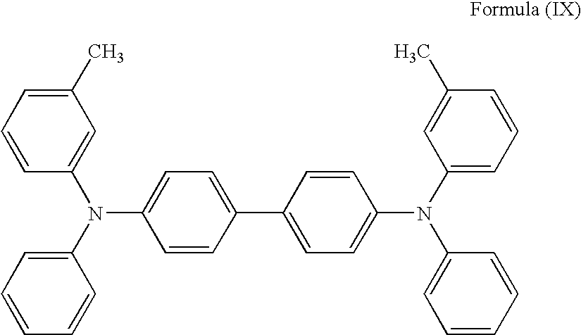
The following can be used for the aromatic tertiary amine contained in the polymer compound as described above: aromatic diamine compounds wherein aromatic tertiary amine units of 1,1-bis{4-(di-p-tolylamine)phenyl}cyclohexane are linked to each other (JP-A No. 59-194393); aromatic amines containing two or more tertiary amines, a typical example of which is 4,4-bis[(N-1-naphthyl)-N-phenylamino]biphenyl (JP-A No. 5-234681); aromatic amines which are derived from triphenylbenezene and have a star-burst structure (U.S. Pat. No. 4,923,774); aromatic amines such as N,N′-diphenyl-N,N′-bis(3-methylphenyl)-(1,1′-biphenyl)-4,4′-diamine (U.S. Pat. No. 4,764,625); α,α,α′,α′-tetramethyl-α,α′-bis(4-di-p-triaminophenyl)-p-xylene (JP-A No. 3-269084); three-dimensionally asymmetric triphenylamine derivatives (JP-A No. 4-129271); compounds having a pyrenyl group substituted with plural aromatic diamine groups (JP-A No. 4-175395); aromatic diamines wherein aromatic tertiary amines are linked to each other through an ethylene group (JP-A No. 4-264189); aromatic diamines having a styryl group (JP-A No. 4-290851); compounds wherein aromatic tertiary amines are linked to each other through a thiophene group (JP-A No. 4-304466); star-burst type aromatic triamines (JP-A No. 4-308688); compounds wherein tertiary amines are linked to each other through a fluorene group (JP-A No. 5-25473); aromatic diamines having a phenoxazine skeleton (JP-A No. 5-290728); and others.
The aromatic tertiary amine preferably contains an aromatic component comprising at least one of a condensed aromatic ring and a polynuclear aromatic ring, bonded to a tertiary amine nitrogen atom thereof.
The aromatic tertiary amine may be incorporated, as a repeating unit, in the main chain structure of the polymer compound.
In this case, the polymer compound used in the invention preferably includes a repeating unit containing, as its partial structure, at least one selected from the following formulae (I-1) and (I-2). Since this kind of polymer compound has better solubility in and compatibility with solvent or resin, an organic semiconductor transistor element with this kind of compound can be produced more easily. Furthermore, the carrier-transporting property of the organic semiconductor transistor element can be improved.
Figure US07166859-20070123-C00001
In the formulae (I-1) and (I-2), Ar represents a substituted or unsubstituted monovalent benzene ring, a substituted or unsubstituted monovalent polynuclear aromatic hydrocarbon having 2 to 10 aromatic rings, a substituted or unsubstituted monovalent condensed aromatic hydrocarbon having 2 to 10 aromatic rings, or a substituted or unsubstituted monovalent aromatic heteroring; X represents a substituted or unsubstituted bivalent benzene ring, a substituted or unsubstituted bivalent polynuclear aromatic hydrocarbon having 2 to 10 aromatic rings, a substituted or unsubstituted bivalent condensed aromatic hydrocarbon having 2 to 10 aromatic rings, or a substituted or unsubstituted bivalent aromatic heteroring; T represents a bivalent straight-chain hydrocarbon group having 1 to 6 carbon atoms, or a bivalent branched hydrocarbon group having 2 to 10 carbon atoms; and k, i, and j each independently represent an integer of 0 or 1.
Specifically, the polynuclear aromatic hydrocarbon and the condensed aromatic hydrocarbon used in the invention are aromatic hydrocarbons as defined per the following:
The “polynuclear aromatic hydrocarbon” is a hydrocarbon wherein two or more aromatic rings composed of carbon and hydrogen atoms are present and the aromatic rings are bonded to each other through carbon-carbon bonds. Specific examples thereof include biphenyl and terphenyl. The “condensed aromatic hydrocarbon” is a hydrocarbon wherein two or more aromatic rings composed of carbon and hydrogen atoms are present and the aromatic rings have a pair of carbon atoms in common. Specific examples thereof include naphthalene, anthracene, and phenanthrene, and fluorene.
Regarding the heteroring, the number (Nr) of atoms constituting the cyclic skeleton thereof is preferably 5 or 6. The kind and the number of atoms (heteroatoms) other than carbon atoms which is contained in the ring are not particularly limited. For example, a sulfur, nitrogen, oxygen or some other atom is preferably used. The ring skeleton may contain two kinds of heteroatoms and/or two or more heteroatoms. In particular, thiophene, pyrrole, furan or a heteroring wherein the carbon atom at the 3- or 4-position of the compound is substituted with a nitrogen atom is preferably used as the heteroring having a 5-membered ring structure, and pyridine is preferably used as the heteroring having a 6-membered ring structure.
Examples of the substituent of the benzene ring, the polynuclear aromatic hydrocarbon, or the condensed aromatic hydrocarbon include hydrogen and halogen atoms; and alkyl, alkoxy, aryl, aralkyl, and substituted amino groups. The alkyl group is preferably an alkyl group having 1 to 10 carbon atoms, examples of which include methyl, ethyl, propyl, and isopropyl groups. The alkoxy group is preferably an alkoxy group having 1 to 10 carbon atoms, examples of which include methoxy, ethoxy, propoxy, and isopropoxy groups. The aryl group is preferably an aryl group having 6 to 20 carbon atoms, examples of which include phenyl, and toluyl groups. The aralkyl group is preferably an aralkyl group having 7 to 20 carbon atoms, examples of which include benzyl, and phenethyl groups. Examples of the substituent of the substituted amino group include alkyl, aryl and aralkyl groups. Specific examples thereof are the same as described above.
X represents a substituted or unsubstituted bivalent benzene ring, a substituted or unsubstituted polynuclear aromatic hydrocarbon having 2 to 10 aromatic rings, a substituted or unsubstituted bivalent condensed aromatic hydrocarbon having 2 to 10 aromatic rings, or a substituted or unsubstituted bivalent aromatic heteroring. X is specifically a group represented by any one selected from the following formulae (1) to (13):
Figure US07166859-20070123-C00002
Figure US07166859-20070123-C00003
In the formulae (1) to (13), R1 to R14 each independently represent a hydrogen atom, an alkyl group having 1 to 10 carbon atoms, an alkoxy group having 1 to 10 carbon atoms, a substituted or unsubstituted phenyl group, a substituted or unsubstituted aralkyl group or a halogen atom; a is 0 or 1; b is an integer from 0 to 10; and V is a group represented by any one selected from the following formulae (14) to (34):
Figure US07166859-20070123-C00004
Figure US07166859-20070123-C00005
In the formulae (14) to (34), R15 represents a hydrogen atom, or an alkyl or cyano group; R16 and R17 each represent a hydrogen atom, an alkyl group having 1 to 10 carbon atoms, an alkoxy group having 1 to 10 carbon atoms, a substituted or unsubstituted phenyl group, a substituted or unsubstituted aralkyl group or a halogen atom; and c is an integer from 0 to 10.
T represents a bivalent straight-chain hydrocarbon group having 1 to 6 carbon atoms or a bivalent branched hydrocarbon group having 2 to 10 carbon atoms, and preferably represents a bivalent normal hydrocarbon group having 2 to 6 carbon atoms or a bivalent branched hydrocarbon group having 3 to 7 carbon atoms. Specific structural examples thereof are illustrated below.
Figure US07166859-20070123-C00006
Figure US07166859-20070123-C00007
Specific examples of the structure represented by the formula (I-1) are shown in Tables 1 to 51, and specific examples of the structure represented by the formula (I-2) are shown in Tables 52 to 101.
TABLE 1
Bonding
Structure k X Ar Position i j T
1 0
Figure US07166859-20070123-C00008
Figure US07166859-20070123-C00009
3 0 0
2 0
Figure US07166859-20070123-C00010
Figure US07166859-20070123-C00011
4 1 1 —CH2CH2
3 0
Figure US07166859-20070123-C00012
Figure US07166859-20070123-C00013
3 0 1 —CH2CH2
4 0
Figure US07166859-20070123-C00014
Figure US07166859-20070123-C00015
4 0 1
Figure US07166859-20070123-C00016
5 0
Figure US07166859-20070123-C00017
Figure US07166859-20070123-C00018
4 0 1
Figure US07166859-20070123-C00019
6 0
Figure US07166859-20070123-C00020
Figure US07166859-20070123-C00021
4 0 1 —CH2CH2
7 0
Figure US07166859-20070123-C00022
Figure US07166859-20070123-C00023
4 0 1 —CH2CH2
8 0
Figure US07166859-20070123-C00024
Figure US07166859-20070123-C00025
4 0 1 —CH2

TABLE 2
Bonding
Structure k X Ar Position i j T
 9 0
Figure US07166859-20070123-C00026
Figure US07166859-20070123-C00027
4 0 1 —CH2CH2
10 0
Figure US07166859-20070123-C00028
Figure US07166859-20070123-C00029
4 1 0
11 0
Figure US07166859-20070123-C00030
Figure US07166859-20070123-C00031
4 0 1 —CH2
12 0
Figure US07166859-20070123-C00032
Figure US07166859-20070123-C00033
4 0 1 —CH2CH2
13 0
Figure US07166859-20070123-C00034
Figure US07166859-20070123-C00035
4 0 1 —CH2
14 0
Figure US07166859-20070123-C00036
Figure US07166859-20070123-C00037
4 0 1 —CH2CH2
15 0
Figure US07166859-20070123-C00038
Figure US07166859-20070123-C00039
4 0 1
Figure US07166859-20070123-C00040

TABLE 3
Bonding
Structure k X Ar Position i j T
16 0
Figure US07166859-20070123-C00041
Figure US07166859-20070123-C00042
4 0 1 —CH2
17 0
Figure US07166859-20070123-C00043
Figure US07166859-20070123-C00044
4 0 1 —CH2CH2
18 0
Figure US07166859-20070123-C00045
Figure US07166859-20070123-C00046
4 0 1 —CH2CH2
19 0
Figure US07166859-20070123-C00047
Figure US07166859-20070123-C00048
4 0 1 —CH2CH2

TABLE 4
Bonding
Structure k X Ar Position i j T
20 0
Figure US07166859-20070123-C00049
Figure US07166859-20070123-C00050
4 0 1 —CH2CH2
21 0
Figure US07166859-20070123-C00051
Figure US07166859-20070123-C00052
3 0 1 —CH2CH2
22 0
Figure US07166859-20070123-C00053
Figure US07166859-20070123-C00054
4 0 1 —CH2CH2
23 0
Figure US07166859-20070123-C00055
Figure US07166859-20070123-C00056
4 0 1
Figure US07166859-20070123-C00057
24 0
Figure US07166859-20070123-C00058
Figure US07166859-20070123-C00059
4 0 1 —CH2CH2
25 0
Figure US07166859-20070123-C00060
Figure US07166859-20070123-C00061
4 0 1 —CH2CH2
26 0
Figure US07166859-20070123-C00062
Figure US07166859-20070123-C00063
4 0 1 —CH2

TABLE 5
Bonding
Structure k X Ar Position i j T
27 0
Figure US07166859-20070123-C00064
Figure US07166859-20070123-C00065
4 0 0
28 0
Figure US07166859-20070123-C00066
Figure US07166859-20070123-C00067
4 1 0
29 0
Figure US07166859-20070123-C00068
Figure US07166859-20070123-C00069
4 0 1 —CH2CH2
30 0
Figure US07166859-20070123-C00070
Figure US07166859-20070123-C00071
4 1 0
31 0
Figure US07166859-20070123-C00072
Figure US07166859-20070123-C00073
4 0 0
32 0
Figure US07166859-20070123-C00074
Figure US07166859-20070123-C00075
4 0 0
33 0
Figure US07166859-20070123-C00076
Figure US07166859-20070123-C00077
4 0 0

TABLE 6
Bonding
Structure k X Ar Position i j T
34 0
Figure US07166859-20070123-C00078
Figure US07166859-20070123-C00079
4 0 0
35 0
Figure US07166859-20070123-C00080
Figure US07166859-20070123-C00081
4 0 0
36 0
Figure US07166859-20070123-C00082
Figure US07166859-20070123-C00083
3 1 1 —CH2CH2
37 0
Figure US07166859-20070123-C00084
Figure US07166859-20070123-C00085
4 1 1 —CH2
38 0
Figure US07166859-20070123-C00086
Figure US07166859-20070123-C00087
4 1 1 —CH2CH2
39 0
Figure US07166859-20070123-C00088
Figure US07166859-20070123-C00089
4 1 1 —CH2
40 0
Figure US07166859-20070123-C00090
Figure US07166859-20070123-C00091
4 1 1 —CH2
41 1
Figure US07166859-20070123-C00092
Figure US07166859-20070123-C00093
4 0 1 —CH2CH2

TABLE 7
Struc- Bonding
ture k X Ar Position i j T
42 1
Figure US07166859-20070123-C00094
Figure US07166859-20070123-C00095
4 0 1 —CH2CH2
43 1
Figure US07166859-20070123-C00096
Figure US07166859-20070123-C00097
4 0 1 —CH2CH2
44 1
Figure US07166859-20070123-C00098
Figure US07166859-20070123-C00099
4 0 1 —CH2CH2
45 1
Figure US07166859-20070123-C00100
Figure US07166859-20070123-C00101
4 0 1 —CH2CH2
46 1
Figure US07166859-20070123-C00102
Figure US07166859-20070123-C00103
4 0 1 —CH2CH2
47 1
Figure US07166859-20070123-C00104
Figure US07166859-20070123-C00105
4 0 1 —CH2

TABLE 8
Bonding
Structure k X Ar Position i j T
48 1
Figure US07166859-20070123-C00106
Figure US07166859-20070123-C00107
4 0 1
Figure US07166859-20070123-C00108
49 1
Figure US07166859-20070123-C00109
Figure US07166859-20070123-C00110
4 0 1
Figure US07166859-20070123-C00111
50 1
Figure US07166859-20070123-C00112
Figure US07166859-20070123-C00113
4 0 1 —CH2CH2
51 1
Figure US07166859-20070123-C00114
Figure US07166859-20070123-C00115
4 0 1 —CH2CH2
52 1
Figure US07166859-20070123-C00116
Figure US07166859-20070123-C00117
4 0 1 —CH2CH2

TABLE 9
Bonding
Structure k X Ar Position i j T
53 1
Figure US07166859-20070123-C00118
Figure US07166859-20070123-C00119
4 0 1 —CH2CH2
54 1
Figure US07166859-20070123-C00120
Figure US07166859-20070123-C00121
2 0 1 —CH2CH2
55 1
Figure US07166859-20070123-C00122
Figure US07166859-20070123-C00123
3 0 1 —CH2CH2
56 1
Figure US07166859-20070123-C00124
Figure US07166859-20070123-C00125
4 0 1 —CH2
57 1
Figure US07166859-20070123-C00126
Figure US07166859-20070123-C00127
4 0 1 —CH2CH2
58 1
Figure US07166859-20070123-C00128
Figure US07166859-20070123-C00129
4 0 1
Figure US07166859-20070123-C00130
59 1
Figure US07166859-20070123-C00131
Figure US07166859-20070123-C00132
4 0 1
Figure US07166859-20070123-C00133

TABLE 10
Bond-
ing
Struc- Posi-
ture k X Ar tion i j T
60 1
Figure US07166859-20070123-C00134
Figure US07166859-20070123-C00135
4 0 1 —CH2CH2
61 1
Figure US07166859-20070123-C00136
Figure US07166859-20070123-C00137
4 0 1 —CH2CH2
62 1
Figure US07166859-20070123-C00138
Figure US07166859-20070123-C00139
3 0 1 —CH2CH2
63 1
Figure US07166859-20070123-C00140
Figure US07166859-20070123-C00141
4 0 1 —CH2CH2
64 1
Figure US07166859-20070123-C00142
Figure US07166859-20070123-C00143
4 0 1
Figure US07166859-20070123-C00144
65 1
Figure US07166859-20070123-C00145
Figure US07166859-20070123-C00146
3 0 1 —CH2CH2
66 1
Figure US07166859-20070123-C00147
Figure US07166859-20070123-C00148
4 0 1 —CH2CH2

TABLE 11
Structure k X Ar Bonding Position i j T
67 1
Figure US07166859-20070123-C00149
Figure US07166859-20070123-C00150
4 0 1
Figure US07166859-20070123-C00151
68 1
Figure US07166859-20070123-C00152
Figure US07166859-20070123-C00153
4 0 1 —CH2CH2
69 1
Figure US07166859-20070123-C00154
Figure US07166859-20070123-C00155
4 0 1
Figure US07166859-20070123-C00156
70 1
Figure US07166859-20070123-C00157
Figure US07166859-20070123-C00158
4 0 1 —CH2CH2
71 1
Figure US07166859-20070123-C00159
Figure US07166859-20070123-C00160
4 0 1 —CH2CH2
72 1
Figure US07166859-20070123-C00161
Figure US07166859-20070123-C00162
4 0 1 —CH2CH2
73 1
Figure US07166859-20070123-C00163
Figure US07166859-20070123-C00164
3 0 1 —CH2

TABLE 12
Bonding
Structure k X Ar Position i j T
74 1
Figure US07166859-20070123-C00165
Figure US07166859-20070123-C00166
3 0 1 —CH2CH2
75 1
Figure US07166859-20070123-C00167
Figure US07166859-20070123-C00168
4 0 0
76 1
Figure US07166859-20070123-C00169
Figure US07166859-20070123-C00170
4 0 0
77 1
Figure US07166859-20070123-C00171
Figure US07166859-20070123-C00172
4 0 0
78 1
Figure US07166859-20070123-C00173
Figure US07166859-20070123-C00174
4 0 0
79 1
Figure US07166859-20070123-C00175
Figure US07166859-20070123-C00176
4 0 0
80 1
Figure US07166859-20070123-C00177
Figure US07166859-20070123-C00178
4 0 1 —CH2

TABLE 13
Bonding
Structure k X Ar Position i j T
81 1
Figure US07166859-20070123-C00179
Figure US07166859-20070123-C00180
4 0 1 —CH2
82 1
Figure US07166859-20070123-C00181
Figure US07166859-20070123-C00182
4 0 1 —CH2
83 1
Figure US07166859-20070123-C00183
Figure US07166859-20070123-C00184
4 0 1 —CH2
84 1
Figure US07166859-20070123-C00185
Figure US07166859-20070123-C00186
4 0 1 —CH2
85 1
Figure US07166859-20070123-C00187
Figure US07166859-20070123-C00188
4 0 1 —CH2CH2
86 1
Figure US07166859-20070123-C00189
Figure US07166859-20070123-C00190
4 0 1 —CH2CH2
87 1
Figure US07166859-20070123-C00191
Figure US07166859-20070123-C00192
4 0 1 —CH2CH2

TABLE 14
Bonding
Structure k X Ar Position i j T
88 1
Figure US07166859-20070123-C00193
Figure US07166859-20070123-C00194
4 0 1 —CH2CH2
89 1
Figure US07166859-20070123-C00195
Figure US07166859-20070123-C00196
4 0 1 —CH2CH2
90 1
Figure US07166859-20070123-C00197
Figure US07166859-20070123-C00198
4 0 1 —CH2CH2
91 1
Figure US07166859-20070123-C00199
Figure US07166859-20070123-C00200
4 0 1 —CH2CH2
92 1
Figure US07166859-20070123-C00201
Figure US07166859-20070123-C00202
4 0 1 —CH2CH2
93 1
Figure US07166859-20070123-C00203
Figure US07166859-20070123-C00204
4 0 1 —CH2CH2

TABLE 15
Bond-
Struc- ing
ture k X Ar Position i j T
94 1
Figure US07166859-20070123-C00205
Figure US07166859-20070123-C00206
4 0 1 —CH2CH2
95 1
Figure US07166859-20070123-C00207
Figure US07166859-20070123-C00208
4 0 1 —CH2CH2
96 1
Figure US07166859-20070123-C00209
Figure US07166859-20070123-C00210
4 0 1
Figure US07166859-20070123-C00211
97 1
Figure US07166859-20070123-C00212
Figure US07166859-20070123-C00213
4 0 1
Figure US07166859-20070123-C00214
98 1
Figure US07166859-20070123-C00215
Figure US07166859-20070123-C00216
4 0 1 —CH2CH2
99 1
Figure US07166859-20070123-C00217
Figure US07166859-20070123-C00218
4 0 1 —CH2CH2

TABLE 16
Bond-
Struc- ing
ture k X Ar Position i j T
100 1
Figure US07166859-20070123-C00219
Figure US07166859-20070123-C00220
4 0 1 —CH2
101 1
Figure US07166859-20070123-C00221
Figure US07166859-20070123-C00222
4 0 1 —CH2CH2
102 1
Figure US07166859-20070123-C00223
Figure US07166859-20070123-C00224
4 0 1 —CH2CH2
103 1
Figure US07166859-20070123-C00225
Figure US07166859-20070123-C00226
4 0 1 —CH2CH2
104 1
Figure US07166859-20070123-C00227
Figure US07166859-20070123-C00228
4 0 1 —CH2CH2
105 1
Figure US07166859-20070123-C00229
Figure US07166859-20070123-C00230
4 0 1 —CH2CH2
106 1
Figure US07166859-20070123-C00231
Figure US07166859-20070123-C00232
4 0 1
Figure US07166859-20070123-C00233

TABLE 17
Structure k X Ar Bonding Position i j T
107 1
Figure US07166859-20070123-C00234
Figure US07166859-20070123-C00235
4 0 1 —CH2CH2
108 1
Figure US07166859-20070123-C00236
Figure US07166859-20070123-C00237
4 0 1 —CH2
109 1
Figure US07166859-20070123-C00238
Figure US07166859-20070123-C00239
4 0 1 —CH2CH2
110 1
Figure US07166859-20070123-C00240
Figure US07166859-20070123-C00241
4 0 0
111 1
Figure US07166859-20070123-C00242
Figure US07166859-20070123-C00243
4 0 0
112 1
Figure US07166859-20070123-C00244
Figure US07166859-20070123-C00245
4 0 0
113 1
Figure US07166859-20070123-C00246
Figure US07166859-20070123-C00247
4 0 0

TABLE 18
Structure k X Ar Bonding Position i j T
114 1
Figure US07166859-20070123-C00248
Figure US07166859-20070123-C00249
4 0 0
115 1
Figure US07166859-20070123-C00250
Figure US07166859-20070123-C00251
4 0 1 —CH2
116 1
Figure US07166859-20070123-C00252
Figure US07166859-20070123-C00253
4 0 1 —CH2
117 1
Figure US07166859-20070123-C00254
Figure US07166859-20070123-C00255
4 0 1 —CH2
118 1
Figure US07166859-20070123-C00256
Figure US07166859-20070123-C00257
4 0 1 —CH2
119 1
Figure US07166859-20070123-C00258
Figure US07166859-20070123-C00259
4 0 1 —CH2
120 1
Figure US07166859-20070123-C00260
Figure US07166859-20070123-C00261
4 0 1 —CH2CH2

TABLE 19
Bonding
Structure k X Ar Position i j T
121 1
Figure US07166859-20070123-C00262
Figure US07166859-20070123-C00263
4 0 1 —CH2
122 1
Figure US07166859-20070123-C00264
Figure US07166859-20070123-C00265
4 1 1 —CH2CH2
123 1
Figure US07166859-20070123-C00266
Figure US07166859-20070123-C00267
4 0 1 —CH2CH2
124 1
Figure US07166859-20070123-C00268
Figure US07166859-20070123-C00269
4 0 1
Figure US07166859-20070123-C00270
125 1
Figure US07166859-20070123-C00271
Figure US07166859-20070123-C00272
4 0 0
126 1
Figure US07166859-20070123-C00273
Figure US07166859-20070123-C00274
4 0 1 —CH2
127 1
Figure US07166859-20070123-C00275
Figure US07166859-20070123-C00276
4 0 1 —CH2CH2

TABLE 20
Bonding
Structure k X Ar Position i j T
128 1
Figure US07166859-20070123-C00277
Figure US07166859-20070123-C00278
4 0 1 —CH2CH2
129 1
Figure US07166859-20070123-C00279
Figure US07166859-20070123-C00280
4 0 1 —CH2CH2
130 1
Figure US07166859-20070123-C00281
Figure US07166859-20070123-C00282
4 0 1 —CH2CH2
131 1
Figure US07166859-20070123-C00283
Figure US07166859-20070123-C00284
4 0 1 —CH2CH2
132 1
Figure US07166859-20070123-C00285
Figure US07166859-20070123-C00286
4 0 1 —CH2CH2
133 1
Figure US07166859-20070123-C00287
Figure US07166859-20070123-C00288
4 0 1 —CH2CH2

TABLE 21
Bonding
Structure k X Ar Position i j T
134 1
Figure US07166859-20070123-C00289
Figure US07166859-20070123-C00290
4 0 1 —CH2CH2
135 1
Figure US07166859-20070123-C00291
Figure US07166859-20070123-C00292
4 0 1 —CH2CH2
136 1
Figure US07166859-20070123-C00293
Figure US07166859-20070123-C00294
4 0 1 —CH2CH2
137 1
Figure US07166859-20070123-C00295
Figure US07166859-20070123-C00296
4 0 1 —CH2CH2
138 1
Figure US07166859-20070123-C00297
Figure US07166859-20070123-C00298
4 0 1
Figure US07166859-20070123-C00299
139 1
Figure US07166859-20070123-C00300
Figure US07166859-20070123-C00301
4 0 1
Figure US07166859-20070123-C00302

TABLE 22
Bonding
Structure k X Ar Position i j T
140 1
Figure US07166859-20070123-C00303
Figure US07166859-20070123-C00304
4 0 1 —CH2CH2
141 1
Figure US07166859-20070123-C00305
Figure US07166859-20070123-C00306
4 0 0
142 1
Figure US07166859-20070123-C00307
Figure US07166859-20070123-C00308
4 0 1 —CH2
143 1
Figure US07166859-20070123-C00309
Figure US07166859-20070123-C00310
3 0 0
144 1
Figure US07166859-20070123-C00311
Figure US07166859-20070123-C00312
4 0 0
145 1
Figure US07166859-20070123-C00313
Figure US07166859-20070123-C00314
4 0 1 —CH2CH2
146 1
Figure US07166859-20070123-C00315
Figure US07166859-20070123-C00316
4 1 0

TABLE 23
Bonding
Structure k X Ar Position i j T
147 1
Figure US07166859-20070123-C00317
Figure US07166859-20070123-C00318
4 0 1 —CH2
148 1
Figure US07166859-20070123-C00319
Figure US07166859-20070123-C00320
4 0 1
Figure US07166859-20070123-C00321
149 1
Figure US07166859-20070123-C00322
Figure US07166859-20070123-C00323
4 0 1 —CH2CH2
150 1
Figure US07166859-20070123-C00324
Figure US07166859-20070123-C00325
4 0 1 —CH2CH2
151 1
Figure US07166859-20070123-C00326
Figure US07166859-20070123-C00327
4 0 1 —CH2CH2
152 1
Figure US07166859-20070123-C00328
Figure US07166859-20070123-C00329
4 0 1 —CH2CH2

TABLE 24
Bonding
Structure k X Ar Position i j T
153 1
Figure US07166859-20070123-C00330
Figure US07166859-20070123-C00331
4 0 1 —CH2CH2
154 1
Figure US07166859-20070123-C00332
Figure US07166859-20070123-C00333
4 0 1 —CH2CH2
155 1
Figure US07166859-20070123-C00334
Figure US07166859-20070123-C00335
4 0 1 —CH2CH2
156 1
Figure US07166859-20070123-C00336
Figure US07166859-20070123-C00337
4 0 1 —CH2CH2
157 1
Figure US07166859-20070123-C00338
Figure US07166859-20070123-C00339
4 0 1 —CH2CH2
158 1
Figure US07166859-20070123-C00340
Figure US07166859-20070123-C00341
4 0 1 —CH2CH2

TABLE 25
Bonding
Structure k X Ar Position i j T
159 1
Figure US07166859-20070123-C00342
Figure US07166859-20070123-C00343
4 0 1 —CH2CH2
160 1
Figure US07166859-20070123-C00344
Figure US07166859-20070123-C00345
4 0 1 —CH2CH2
161 1
Figure US07166859-20070123-C00346
Figure US07166859-20070123-C00347
4 0 1 —CH2CH2
162 1
Figure US07166859-20070123-C00348
Figure US07166859-20070123-C00349
4 0 1 —CH2CH2
163 1
Figure US07166859-20070123-C00350
Figure US07166859-20070123-C00351
4 0 1 —CH2CH2
164 1
Figure US07166859-20070123-C00352
Figure US07166859-20070123-C00353
4 0 1 —CH2CH2

TABLE 26
Bonding
Structure k X Ar Position i j T
165 1
Figure US07166859-20070123-C00354
Figure US07166859-20070123-C00355
4 0 1 —CH2CH2
166 1
Figure US07166859-20070123-C00356
Figure US07166859-20070123-C00357
4 0 1 —CH2CH2
167 1
Figure US07166859-20070123-C00358
Figure US07166859-20070123-C00359
4 0 1 —CH2CH2
168 1
Figure US07166859-20070123-C00360
Figure US07166859-20070123-C00361
4 0 1 —CH2CH2
169 1
Figure US07166859-20070123-C00362
Figure US07166859-20070123-C00363
4 0 1 —CH2CH2
170 1
Figure US07166859-20070123-C00364
Figure US07166859-20070123-C00365
4 0 1 —CH2CH2

TABLE 27
Bonding
Structure k X Ar Position i j T
171 1
Figure US07166859-20070123-C00366
Figure US07166859-20070123-C00367
4 0 0
172 1
Figure US07166859-20070123-C00368
Figure US07166859-20070123-C00369
4 0 1 —CH2
173 1
Figure US07166859-20070123-C00370
Figure US07166859-20070123-C00371
4 0 0
174 1
Figure US07166859-20070123-C00372
Figure US07166859-20070123-C00373
4 1 0
175 1
Figure US07166859-20070123-C00374
Figure US07166859-20070123-C00375
4 0 1 —CH2CH2
176 1
Figure US07166859-20070123-C00376
Figure US07166859-20070123-C00377
4 0 1 —CH2CH2

TABLE 28
Bonding
Structure k X Ar Position i j T
177 1
Figure US07166859-20070123-C00378
Figure US07166859-20070123-C00379
4 0 1 —CH2CH2
178 1
Figure US07166859-20070123-C00380
Figure US07166859-20070123-C00381
4 0 1 —CH2CH2
179 1
Figure US07166859-20070123-C00382
Figure US07166859-20070123-C00383
4 0 1 —CH2CH2
180 1
Figure US07166859-20070123-C00384
Figure US07166859-20070123-C00385
4 0 1 —CH2CH2
181 1
Figure US07166859-20070123-C00386
Figure US07166859-20070123-C00387
4 0 1 —CH2CH2

TABLE 29
Bonding
Structure k X Ar Position i j T
182 1
Figure US07166859-20070123-C00388
Figure US07166859-20070123-C00389
4 0 1 —CH2CH2
183 1
Figure US07166859-20070123-C00390
Figure US07166859-20070123-C00391
4 0 1 —CH2CH2
184 1
Figure US07166859-20070123-C00392
Figure US07166859-20070123-C00393
4 0 1 —CH2CH2
185 1
Figure US07166859-20070123-C00394
Figure US07166859-20070123-C00395
4 0 1 —CH2
186 1
Figure US07166859-20070123-C00396
Figure US07166859-20070123-C00397
4 0 1 —CH2CH2
187 1
Figure US07166859-20070123-C00398
Figure US07166859-20070123-C00399
4 0 1 —CH2CH2
188 1
Figure US07166859-20070123-C00400
Figure US07166859-20070123-C00401
4 0 1 —CH2CH2

TABLE 30
Bond-
Struc- ing
ture k X Ar Position i j T
189 1
Figure US07166859-20070123-C00402
Figure US07166859-20070123-C00403
4 0 1
190 1
Figure US07166859-20070123-C00404
Figure US07166859-20070123-C00405
4 0 1 —CH2
191 1
Figure US07166859-20070123-C00406
Figure US07166859-20070123-C00407
4 0 1 —CH2
192 1
Figure US07166859-20070123-C00408
Figure US07166859-20070123-C00409
4 0 1 —CH2CH2
193 1
Figure US07166859-20070123-C00410
Figure US07166859-20070123-C00411
4 0 1
Figure US07166859-20070123-C00412
194 1
Figure US07166859-20070123-C00413
Figure US07166859-20070123-C00414
4 0 1 —CH2CH2
195 1
Figure US07166859-20070123-C00415
Figure US07166859-20070123-C00416
4 0 1 —CH2CH2

TABLE 31
Bonding
Structure k X Ar Position i j T
196 1
Figure US07166859-20070123-C00417
Figure US07166859-20070123-C00418
4 0 1 —CH2CH2
197 1
Figure US07166859-20070123-C00419
Figure US07166859-20070123-C00420
4 0 1 —CH2CH2
198 1
Figure US07166859-20070123-C00421
Figure US07166859-20070123-C00422
4 0 1 —CH2CH2
199 1
Figure US07166859-20070123-C00423
Figure US07166859-20070123-C00424
4 0 1 —CH2CH2
200 1
Figure US07166859-20070123-C00425
Figure US07166859-20070123-C00426
4 0 1 —CH2CH2
201 1
Figure US07166859-20070123-C00427
Figure US07166859-20070123-C00428
4 0 1 —CH2CH2
202 1
Figure US07166859-20070123-C00429
Figure US07166859-20070123-C00430
4 0 1
Figure US07166859-20070123-C00431

TABLE 32
Bond-
Struc- ing
ture k X Ar Position i j T
203 1
Figure US07166859-20070123-C00432
Figure US07166859-20070123-C00433
4 0 1 —CH2CH2
204 1
Figure US07166859-20070123-C00434
Figure US07166859-20070123-C00435
4 0 1 —CH2CH2
205 1
Figure US07166859-20070123-C00436
Figure US07166859-20070123-C00437
4 0 0
206 1
Figure US07166859-20070123-C00438
Figure US07166859-20070123-C00439
4 0 1 —CH2
207 1
Figure US07166859-20070123-C00440
Figure US07166859-20070123-C00441
4 0 1 —CH2CH2
208 1
Figure US07166859-20070123-C00442
Figure US07166859-20070123-C00443
4 0 1 —CH2CH2
209 1
Figure US07166859-20070123-C00444
Figure US07166859-20070123-C00445
4 0 1 —CH2CH2

TABLE 33
Struc- Bonding
ture k X Ar Position i j T
210 1
Figure US07166859-20070123-C00446
Figure US07166859-20070123-C00447
4 0 1 —CH2CH2
211 1
Figure US07166859-20070123-C00448
Figure US07166859-20070123-C00449
4 0 1 —CH2CH2
212 1
Figure US07166859-20070123-C00450
Figure US07166859-20070123-C00451
4 0 1 —CH2CH2
213 1
Figure US07166859-20070123-C00452
Figure US07166859-20070123-C00453
4 0 1 —CH2CH2
214 1
Figure US07166859-20070123-C00454
Figure US07166859-20070123-C00455
4 0 1 —CH2CH2
215 1
Figure US07166859-20070123-C00456
Figure US07166859-20070123-C00457
4 0 1 —CH2CH2
216 1
Figure US07166859-20070123-C00458
Figure US07166859-20070123-C00459
4 0 1 —CH2CH2

TABLE 34
Bond-
Struc- ing
ture k X Ar Position i j T
217 1
Figure US07166859-20070123-C00460
Figure US07166859-20070123-C00461
4 0 1 —CH2CH2
218 1
Figure US07166859-20070123-C00462
Figure US07166859-20070123-C00463
4 0 0
219 1
Figure US07166859-20070123-C00464
Figure US07166859-20070123-C00465
4 0 1 —CH2
220 1
Figure US07166859-20070123-C00466
Figure US07166859-20070123-C00467
4 0 1 —CH2
221 1
Figure US07166859-20070123-C00468
Figure US07166859-20070123-C00469
4 0 1 —CH2
222 1
Figure US07166859-20070123-C00470
Figure US07166859-20070123-C00471
4 0 0

TABLE 35
Bonding
Structure k X Ar Position i j T
223 1
Figure US07166859-20070123-C00472
Figure US07166859-20070123-C00473
4 0 1
Figure US07166859-20070123-C00474
224 1
Figure US07166859-20070123-C00475
Figure US07166859-20070123-C00476
4 0 1 —CH2CH2
225 1
Figure US07166859-20070123-C00477
Figure US07166859-20070123-C00478
4 0 1 —CH2CH2
226 1
Figure US07166859-20070123-C00479
Figure US07166859-20070123-C00480
4 0 1 —CH2CH2
227 1
Figure US07166859-20070123-C00481
Figure US07166859-20070123-C00482
4 0 1 —CH2CH2
228 1
Figure US07166859-20070123-C00483
Figure US07166859-20070123-C00484
4 0 1 —CH2
229 1
Figure US07166859-20070123-C00485
Figure US07166859-20070123-C00486
4 0 1
Figure US07166859-20070123-C00487

TABLE 36
Bonding
Structure k X Ar Position i j T
230 1
Figure US07166859-20070123-C00488
Figure US07166859-20070123-C00489
4 0 0
231 1
Figure US07166859-20070123-C00490
Figure US07166859-20070123-C00491
4 0 1 —CH2
232 1
Figure US07166859-20070123-C00492
Figure US07166859-20070123-C00493
4 0 1 —CH2CH2
233 1
Figure US07166859-20070123-C00494
Figure US07166859-20070123-C00495
4 0 1 —CH2
234 1
Figure US07166859-20070123-C00496
Figure US07166859-20070123-C00497
4 0 1 —CH2
235 1
Figure US07166859-20070123-C00498
Figure US07166859-20070123-C00499
4 0 1 —CH2

TABLE 37
Bonding
Structure k X Ar Position i j T
236 1
Figure US07166859-20070123-C00500
Figure US07166859-20070123-C00501
4 0 1 —CH2CH2
237 1
Figure US07166859-20070123-C00502
Figure US07166859-20070123-C00503
4 0 1 —CH2
238 1
Figure US07166859-20070123-C00504
Figure US07166859-20070123-C00505
4 0 1 —CH2CH2
239 1
Figure US07166859-20070123-C00506
Figure US07166859-20070123-C00507
4 0 1 —CH2CH2
240 1
Figure US07166859-20070123-C00508
Figure US07166859-20070123-C00509
4 0 1 —CH2CH2
241 1
Figure US07166859-20070123-C00510
Figure US07166859-20070123-C00511
4 0 1 —CH2
242 1
Figure US07166859-20070123-C00512
Figure US07166859-20070123-C00513
4 0 1
Figure US07166859-20070123-C00514

TABLE 38
Bonding
Structure k X Ar Position i j T
243 1
Figure US07166859-20070123-C00515
Figure US07166859-20070123-C00516
4 0 1 —CH2CH2
244 1
Figure US07166859-20070123-C00517
Figure US07166859-20070123-C00518
4 0 1 —CH2
245 1
Figure US07166859-20070123-C00519
Figure US07166859-20070123-C00520
4 0 1 —CH2
246 1
Figure US07166859-20070123-C00521
Figure US07166859-20070123-C00522
4 0 1 —CH2
247 1
Figure US07166859-20070123-C00523
Figure US07166859-20070123-C00524
4 0 1 —CH2CH2
248 1
Figure US07166859-20070123-C00525
Figure US07166859-20070123-C00526
4 0 1 —CH2

TABLE 39
Bonding
Structure k X Ar Position i j T
249 1
Figure US07166859-20070123-C00527
Figure US07166859-20070123-C00528
4 0 1 —CH2CH2
250 1
Figure US07166859-20070123-C00529
Figure US07166859-20070123-C00530
4 0 1 —CH2
251 1
Figure US07166859-20070123-C00531
Figure US07166859-20070123-C00532
4 0 1 —CH2CH2
252 1
Figure US07166859-20070123-C00533
Figure US07166859-20070123-C00534
4 0 1 —CH2
253 1
Figure US07166859-20070123-C00535
Figure US07166859-20070123-C00536
4 0 1 —CH2

TABLE 40
Bonding
Structure k X Ar Position i j T
254 1
Figure US07166859-20070123-C00537
Figure US07166859-20070123-C00538
4 0 1 —CH2
255 1
Figure US07166859-20070123-C00539
Figure US07166859-20070123-C00540
4 0 1 —CH2CH2
256 1
Figure US07166859-20070123-C00541
Figure US07166859-20070123-C00542
4 1 1 —CH2
257 1
Figure US07166859-20070123-C00543
Figure US07166859-20070123-C00544
4 0 1 —CH2
258 1
Figure US07166859-20070123-C00545
Figure US07166859-20070123-C00546
4 0 1 —CH2CH2

TABLE 41
Bonding
Structure k X Ar Position i j T
259 1
Figure US07166859-20070123-C00547
Figure US07166859-20070123-C00548
4 0 1 —CH2
260 1
Figure US07166859-20070123-C00549
Figure US07166859-20070123-C00550
4 0 1 —CH2CH2
261 1
Figure US07166859-20070123-C00551
Figure US07166859-20070123-C00552
4 0 1
Figure US07166859-20070123-C00553
262 1
Figure US07166859-20070123-C00554
Figure US07166859-20070123-C00555
4 0 1 —CH2CH2
263 1
Figure US07166859-20070123-C00556
Figure US07166859-20070123-C00557
4 0 1 —CH2CH2

TABLE 42
Bonding
Structure k X Ar Position i j T
264 1
Figure US07166859-20070123-C00558
Figure US07166859-20070123-C00559
4 0 1 —CH2
265 1
Figure US07166859-20070123-C00560
Figure US07166859-20070123-C00561
4 0 1 —CH2CH2
266 1
Figure US07166859-20070123-C00562
Figure US07166859-20070123-C00563
4 0 1 —CH2
267 1
Figure US07166859-20070123-C00564
Figure US07166859-20070123-C00565
4 0 1 —CH2CH2

TABLE 43
Bonding
Structure k X Ar Position i j T
268 1
Figure US07166859-20070123-C00566
Figure US07166859-20070123-C00567
4 0 1 —CH2
269 1
Figure US07166859-20070123-C00568
Figure US07166859-20070123-C00569
4 0 1 —CH2CH2
270 1
Figure US07166859-20070123-C00570
Figure US07166859-20070123-C00571
4 0 1 —CH2CH2
271 1
Figure US07166859-20070123-C00572
Figure US07166859-20070123-C00573
4 0 1 —CH2CH2

TABLE 44
Bonding
Structure k X Ar Position i j T
272 1
Figure US07166859-20070123-C00574
Figure US07166859-20070123-C00575
4 0 1 —CH2CH2
273 1
Figure US07166859-20070123-C00576
Figure US07166859-20070123-C00577
4 0 1 —CH2CH2
274 1
Figure US07166859-20070123-C00578
Figure US07166859-20070123-C00579
4 0 1 —CH2CH2

TABLE 45
Bonding
Structure k X Ar Position i j T
275 1
Figure US07166859-20070123-C00580
Figure US07166859-20070123-C00581
4 0 1 —CH2CH2
276 1
Figure US07166859-20070123-C00582
Figure US07166859-20070123-C00583
4 0 1 —CH2
277 1
Figure US07166859-20070123-C00584
Figure US07166859-20070123-C00585
4 0 1 —CH2
278 1
Figure US07166859-20070123-C00586
Figure US07166859-20070123-C00587
4 0 1 —CH2CH2

TABLE 46
Struc- Bonding
ture k X Ar Position i j T
279 1
Figure US07166859-20070123-C00588
Figure US07166859-20070123-C00589
4 0 1 —CH2
280 1
Figure US07166859-20070123-C00590
Figure US07166859-20070123-C00591
4 0 1 —CH2CH2
281 1
Figure US07166859-20070123-C00592
Figure US07166859-20070123-C00593
4 0 1 —CH2CH2
282 1
Figure US07166859-20070123-C00594
Figure US07166859-20070123-C00595
4 0 1 —CH2CH2

TABLE 47
Bond-
ing
Struc- Posi-
ture k X Ar tion i j T
283 1
Figure US07166859-20070123-C00596
Figure US07166859-20070123-C00597
4 0 1 —CH2CH2
284 1
Figure US07166859-20070123-C00598
Figure US07166859-20070123-C00599
4 0 1 —CH2CH2
285 1
Figure US07166859-20070123-C00600
Figure US07166859-20070123-C00601
4 0 1 —CH2CH2
286 1
Figure US07166859-20070123-C00602
Figure US07166859-20070123-C00603
4 0 1 —CH2CH2

TABLE 48
Bonding
Structure k X Ar Position i j T
287 1
Figure US07166859-20070123-C00604
Figure US07166859-20070123-C00605
4 0 1 —CH2CH2
288 1
Figure US07166859-20070123-C00606
Figure US07166859-20070123-C00607
4 0 1 —CH2CH2
289 1
Figure US07166859-20070123-C00608
Figure US07166859-20070123-C00609
4 0 1 —CH2
290 1
Figure US07166859-20070123-C00610
Figure US07166859-20070123-C00611
4 0 1
Figure US07166859-20070123-C00612

TABLE 49
Bond-
ing
Struc- Posi-
ture k X Ar tion i j T
291 1
Figure US07166859-20070123-C00613
Figure US07166859-20070123-C00614
4 0 1 —CH2CH2
292 1
Figure US07166859-20070123-C00615
Figure US07166859-20070123-C00616
4 0 1 —CH2CH2
293 1
Figure US07166859-20070123-C00617
Figure US07166859-20070123-C00618
4 0 1 —CH2CH2
294 1
Figure US07166859-20070123-C00619
Figure US07166859-20070123-C00620
4 0 1 —CH2

TABLE 50
Struc- Bonding
ture k X Ar Position i j T
295 1
Figure US07166859-20070123-C00621
Figure US07166859-20070123-C00622
4 0 1 —CH2
296 1
Figure US07166859-20070123-C00623
Figure US07166859-20070123-C00624
4 0 1 —CH2
297 1
Figure US07166859-20070123-C00625
Figure US07166859-20070123-C00626
4 0 1 —CH2CH2
298 1
Figure US07166859-20070123-C00627
Figure US07166859-20070123-C00628
4 0 1 —CH2CH2

TABLE 51
Bonding
Structure k X Ar Position i j T
299 1
Figure US07166859-20070123-C00629
Figure US07166859-20070123-C00630
4 0 1 —CH2
300 1
Figure US07166859-20070123-C00631
Figure US07166859-20070123-C00632
4 0 1
Figure US07166859-20070123-C00633
301 1
Figure US07166859-20070123-C00634
Figure US07166859-20070123-C00635
4 0 1 —CH2CH2
302 1
Figure US07166859-20070123-C00636
Figure US07166859-20070123-C00637
4 0 1 —CH2CH2

TABLE 52
Bonding
Structure k X Ar Position i j T
303 0
Figure US07166859-20070123-C00638
Figure US07166859-20070123-C00639
4,4 0 0
304 0
Figure US07166859-20070123-C00640
Figure US07166859-20070123-C00641
4,4 1 1 —CH2CH2
305 0
Figure US07166859-20070123-C00642
Figure US07166859-20070123-C00643
4,4 0 1 —CH2CH2
306 0
Figure US07166859-20070123-C00644
Figure US07166859-20070123-C00645
4,4 0 1
Figure US07166859-20070123-C00646
307 0
Figure US07166859-20070123-C00647
Figure US07166859-20070123-C00648
4,4 0 1 —CH2CH2
308 0
Figure US07166859-20070123-C00649
Figure US07166859-20070123-C00650
4,4 0 1
Figure US07166859-20070123-C00651
309 0
Figure US07166859-20070123-C00652
Figure US07166859-20070123-C00653
4,4 0 1 —CH2CH2

TABLE 53
Bonding
Structure k X Ar Position i j T
310 0
Figure US07166859-20070123-C00654
Figure US07166859-20070123-C00655
4,4 0 1 —CH2
311 0
Figure US07166859-20070123-C00656
Figure US07166859-20070123-C00657
4,4 0 1 —CH2CH2
312 0
Figure US07166859-20070123-C00658
Figure US07166859-20070123-C00659
4,4 0 1 —CH2CH2
313 0
Figure US07166859-20070123-C00660
Figure US07166859-20070123-C00661
4,4 0 1 —CH2
314 0
Figure US07166859-20070123-C00662
Figure US07166859-20070123-C00663
4,4 0 1 —CH2CH2
315 0
Figure US07166859-20070123-C00664
Figure US07166859-20070123-C00665
4,4 0 1
Figure US07166859-20070123-C00666

TABLE 54
Bonding
Structure k X Ar Position i j T
316 0
Figure US07166859-20070123-C00667
Figure US07166859-20070123-C00668
4,4 0 1 —CH2
317 0
Figure US07166859-20070123-C00669
Figure US07166859-20070123-C00670
4,4 0 1 —CH2CH2
318 0
Figure US07166859-20070123-C00671
Figure US07166859-20070123-C00672
4,4 0 1 —CH2CH2
319 0
Figure US07166859-20070123-C00673
Figure US07166859-20070123-C00674
4,4 0 1 —CH2CH2

TABLE 55
Bonding
Structure k X Ar Position i j T
320 0
Figure US07166859-20070123-C00675
Figure US07166859-20070123-C00676
4,4 0 1 —CH2CH2
321 0
Figure US07166859-20070123-C00677
Figure US07166859-20070123-C00678
4,4 0 1 —CH2CH2
322 0
Figure US07166859-20070123-C00679
Figure US07166859-20070123-C00680
4,4 0 1
Figure US07166859-20070123-C00681
323 0
Figure US07166859-20070123-C00682
Figure US07166859-20070123-C00683
4,4 0 1 —CH2CH2
324 0
Figure US07166859-20070123-C00684
Figure US07166859-20070123-C00685
4,4 0 1 —CH2CH2
325 0
Figure US07166859-20070123-C00686
Figure US07166859-20070123-C00687
4,4 0 1 —CH2

TABLE 56
Bonding
Structure k X Ar Position i j T
326 0
Figure US07166859-20070123-C00688
Figure US07166859-20070123-C00689
4,4 0 0
327 0
Figure US07166859-20070123-C00690
Figure US07166859-20070123-C00691
4,4 1 0
328 0
Figure US07166859-20070123-C00692
Figure US07166859-20070123-C00693
4,4 0 1 —CH2CH2
329 0
Figure US07166859-20070123-C00694
Figure US07166859-20070123-C00695
4,4 1 0
Figure US07166859-20070123-C00696
330 0
Figure US07166859-20070123-C00697
Figure US07166859-20070123-C00698
4,4 0 0
331 0
Figure US07166859-20070123-C00699
Figure US07166859-20070123-C00700
4,4 0 0
332 0
Figure US07166859-20070123-C00701
Figure US07166859-20070123-C00702
4,4 0 0

TABLE 57
Bond-
ing
Struc- Posi-
ture k X Ar tion i j T
333 0
Figure US07166859-20070123-C00703
Figure US07166859-20070123-C00704
4,4 0 0
334 0
Figure US07166859-20070123-C00705
Figure US07166859-20070123-C00706
4,4 1 1 —CH2CH2
335 0
Figure US07166859-20070123-C00707
Figure US07166859-20070123-C00708
4,4 1 1 —CH2
336 0
Figure US07166859-20070123-C00709
Figure US07166859-20070123-C00710
4,4 1 1 —CH2CH2
337 0
Figure US07166859-20070123-C00711
Figure US07166859-20070123-C00712
4,4 1 1 —CH2
338 0
Figure US07166859-20070123-C00713
Figure US07166859-20070123-C00714
4,4 1 1 —CH2
339 1
Figure US07166859-20070123-C00715
Figure US07166859-20070123-C00716
4,4 0 1 —CH2CH2

TABLE 58
Bonding
Structure k X Ar Position i j T
340 1
Figure US07166859-20070123-C00717
Figure US07166859-20070123-C00718
4,4 0 1 —CH2CH2
341 1
Figure US07166859-20070123-C00719
Figure US07166859-20070123-C00720
4,4 0 1 —CH2CH2
342 1
Figure US07166859-20070123-C00721
Figure US07166859-20070123-C00722
4,4 0 1 —CH2CH2
343 1
Figure US07166859-20070123-C00723
Figure US07166859-20070123-C00724
4,4 0 1 —CH2CH2
344 1
Figure US07166859-20070123-C00725
Figure US07166859-20070123-C00726
4,4 0 1 —CH2CH2
345 1
Figure US07166859-20070123-C00727
Figure US07166859-20070123-C00728
4,4 0 1 —CH2

TABLE 59
Struc- Bonding
ture k X Ar Position i j T
346 1
Figure US07166859-20070123-C00729
Figure US07166859-20070123-C00730
4,4 0 1
Figure US07166859-20070123-C00731
347 1
Figure US07166859-20070123-C00732
Figure US07166859-20070123-C00733
4,4 0 1
Figure US07166859-20070123-C00734
348 1
Figure US07166859-20070123-C00735
Figure US07166859-20070123-C00736
4,4 0 1 —CH2CH2
349 1
Figure US07166859-20070123-C00737
Figure US07166859-20070123-C00738
4,4 0 1 —CH2CH2
350 1
Figure US07166859-20070123-C00739
Figure US07166859-20070123-C00740
4,4 0 1 —CH2CH2

TABLE 60
Bond-
ing
Struc- Posi-
ture k X Ar tion i j T
351 1
Figure US07166859-20070123-C00741
Figure US07166859-20070123-C00742
4,4 0 1 —CH2CH2
352 1
Figure US07166859-20070123-C00743
Figure US07166859-20070123-C00744
4,4 0 1 —CH2CH2
353 1
Figure US07166859-20070123-C00745
Figure US07166859-20070123-C00746
4,4 0 1
Figure US07166859-20070123-C00747
354 1
Figure US07166859-20070123-C00748
Figure US07166859-20070123-C00749
4,4 0 1
Figure US07166859-20070123-C00750
355 1
Figure US07166859-20070123-C00751
Figure US07166859-20070123-C00752
4,4 0 1 —CH2CH2
356 1
Figure US07166859-20070123-C00753
Figure US07166859-20070123-C00754
4,4 0 1 —CH2CH2
357 1
Figure US07166859-20070123-C00755
Figure US07166859-20070123-C00756
4,4 0 1 —CH2CH2

TABLE 61
Struc- Bonding
ture k X Ar Position i j T
358 1
Figure US07166859-20070123-C00757
Figure US07166859-20070123-C00758
4,4 0 1
Figure US07166859-20070123-C00759
359 1
Figure US07166859-20070123-C00760
Figure US07166859-20070123-C00761
4,4 0 1 —CH2CH2
360 1
Figure US07166859-20070123-C00762
Figure US07166859-20070123-C00763
4,4 0 1
Figure US07166859-20070123-C00764
361 1
Figure US07166859-20070123-C00765
Figure US07166859-20070123-C00766
4,4 0 1
Figure US07166859-20070123-C00767
362 1
Figure US07166859-20070123-C00768
Figure US07166859-20070123-C00769
4,4 0 1 —CH2CH2
363 1
Figure US07166859-20070123-C00770
Figure US07166859-20070123-C00771
4,4 0 1
Figure US07166859-20070123-C00772

TABLE 62
Bonding
Structure k X Ar Position i j T
364 1
Figure US07166859-20070123-C00773
Figure US07166859-20070123-C00774
4,4 0 1 —CH2CH2
365 1
Figure US07166859-20070123-C00775
Figure US07166859-20070123-C00776
4,4 0 1 —CH2CH2
366 1
Figure US07166859-20070123-C00777
Figure US07166859-20070123-C00778
4,4 0 0
367 1
Figure US07166859-20070123-C00779
Figure US07166859-20070123-C00780
4,4 0 1 —CH2CH2
368 1
Figure US07166859-20070123-C00781
Figure US07166859-20070123-C00782
4,4 0 1 —CH2CH2
369 1
Figure US07166859-20070123-C00783
Figure US07166859-20070123-C00784
4,4 0 1 —CH2CH2
370 1
Figure US07166859-20070123-C00785
Figure US07166859-20070123-C00786
4,4 0 0

TABLE 63
Bonding
Structure k X Ar Position i j T
371 1
Figure US07166859-20070123-C00787
Figure US07166859-20070123-C00788
4,4 0 1 —CH2
372 1
Figure US07166859-20070123-C00789
Figure US07166859-20070123-C00790
4,4 0 1 —CH2
373 1
Figure US07166859-20070123-C00791
Figure US07166859-20070123-C00792
4,4 0 1 —CH2
374 1
Figure US07166859-20070123-C00793
Figure US07166859-20070123-C00794
4,4 0 1 —CH2
375 1
Figure US07166859-20070123-C00795
Figure US07166859-20070123-C00796
4,4 0 1 —CH2
376 1
Figure US07166859-20070123-C00797
Figure US07166859-20070123-C00798
4,4 0 1 —CH2CH2

TABLE 64
Struc- Bonding
ture k X Ar Position i j T
377 1
Figure US07166859-20070123-C00799
Figure US07166859-20070123-C00800
4,4 0 1 —CH2CH2
378 1
Figure US07166859-20070123-C00801
Figure US07166859-20070123-C00802
4,4 1 1 —CH2CH2
379 1
Figure US07166859-20070123-C00803
Figure US07166859-20070123-C00804
4,4 0 1 —CH2CH2
380 1
Figure US07166859-20070123-C00805
Figure US07166859-20070123-C00806
4,4 0 1 —CH2CH2
381 1
Figure US07166859-20070123-C00807
Figure US07166859-20070123-C00808
4,4 0 1 —CH2CH2
382 1
Figure US07166859-20070123-C00809
Figure US07166859-20070123-C00810
4,4 0 1 —CH2CH2

TABLE 65
Bond-
ing
Struc- Posi-
ture k X Ar tion i j T
383 1
Figure US07166859-20070123-C00811
Figure US07166859-20070123-C00812
4,4 0 1 —CH2CH2
384 1
Figure US07166859-20070123-C00813
Figure US07166859-20070123-C00814
4,4 0 1 —CH2CH2
385 1
Figure US07166859-20070123-C00815
Figure US07166859-20070123-C00816
4,4 0 1 —CH2CH2
386 1
Figure US07166859-20070123-C00817
Figure US07166859-20070123-C00818
4,4 0 1 —CH2CH2
387 1
Figure US07166859-20070123-C00819
Figure US07166859-20070123-C00820
4,4 0 1
Figure US07166859-20070123-C00821
388 1
Figure US07166859-20070123-C00822
Figure US07166859-20070123-C00823
4,4 0 1
Figure US07166859-20070123-C00824

TABLE 66
Struc- Bonding
ture k X Ar Position i j T
389 1
Figure US07166859-20070123-C00825
Figure US07166859-20070123-C00826
4,4 0 1 —CH2CH2
390 1
Figure US07166859-20070123-C00827
Figure US07166859-20070123-C00828
4,4 0 1 —CH2
391 1
Figure US07166859-20070123-C00829
Figure US07166859-20070123-C00830
4,4 0 1 —CH2CH2
392 1
Figure US07166859-20070123-C00831
Figure US07166859-20070123-C00832
4,4 0 1 —CH2CH2
393 1
Figure US07166859-20070123-C00833
Figure US07166859-20070123-C00834
4,4 0 1 —CH2CH2
394 1
Figure US07166859-20070123-C00835
Figure US07166859-20070123-C00836
4,4 0 1 —CH2CH2
395 1
Figure US07166859-20070123-C00837
Figure US07166859-20070123-C00838
4,4 0 1
Figure US07166859-20070123-C00839

TABLE 67
Bonding
Structure k X Ar Position i j T
396 1
Figure US07166859-20070123-C00840
Figure US07166859-20070123-C00841
4,4 0 1 —CH2CH2
397 1
Figure US07166859-20070123-C00842
Figure US07166859-20070123-C00843
4,4 0 1 —CH2
398 1
Figure US07166859-20070123-C00844
Figure US07166859-20070123-C00845
4,4 0 1 —CH2CH2
399 1
Figure US07166859-20070123-C00846
Figure US07166859-20070123-C00847
4,4 0 1 —CH2CH2
400 1
Figure US07166859-20070123-C00848
Figure US07166859-20070123-C00849
4,4 0 1 —CH2CH2
401 1
Figure US07166859-20070123-C00850
Figure US07166859-20070123-C00851
4,4 0 1 —CH2CH2
402 1
Figure US07166859-20070123-C00852
Figure US07166859-20070123-C00853
4,4 0 1 —CH2CH2

TABLE 68
Struc- Bonding
ture k X Ar Position i j T
403 1
Figure US07166859-20070123-C00854
Figure US07166859-20070123-C00855
4,4 0 1 —CH2CH2
404 1
Figure US07166859-20070123-C00856
Figure US07166859-20070123-C00857
4,4 0 1 —CH2
405 1
Figure US07166859-20070123-C00858
Figure US07166859-20070123-C00859
4,4 0 1 —CH2
406 1
Figure US07166859-20070123-C00860
Figure US07166859-20070123-C00861
4,4 0 1 —CH2
407 1
Figure US07166859-20070123-C00862
Figure US07166859-20070123-C00863
4,4 0 1 —CH2
408 1
Figure US07166859-20070123-C00864
Figure US07166859-20070123-C00865
4,4 0 1 —CH2
409 1
Figure US07166859-20070123-C00866
Figure US07166859-20070123-C00867
4,4 0 1 —CH2CH2

TABLE 69
Bonding
Structure k X Ar Position i j T
410 1
Figure US07166859-20070123-C00868
Figure US07166859-20070123-C00869
4,4 0 1 —CH2
411 1
Figure US07166859-20070123-C00870
Figure US07166859-20070123-C00871
4,4 1 1 —CH2CH2
412 1
Figure US07166859-20070123-C00872
Figure US07166859-20070123-C00873
4,4 0 1 —CH2CH2
413 1
Figure US07166859-20070123-C00874
Figure US07166859-20070123-C00875
4,4 0 1
Figure US07166859-20070123-C00876
414 1
Figure US07166859-20070123-C00877
Figure US07166859-20070123-C00878
4,4 0 0
415 1
Figure US07166859-20070123-C00879
Figure US07166859-20070123-C00880
4,4 0 1 —CH2
416 1
Figure US07166859-20070123-C00881
Figure US07166859-20070123-C00882
4,4 0 1 —CH2CH2

TABLE 70
Bond-
ing
Struc- Posi-
ture k X Ar tion i j T
417 1
Figure US07166859-20070123-C00883
Figure US07166859-20070123-C00884
4,4 0 1 —CH2CH2
418 1
Figure US07166859-20070123-C00885
Figure US07166859-20070123-C00886
4,4 0 1 —CH2CH2
419 1
Figure US07166859-20070123-C00887
Figure US07166859-20070123-C00888
4,4 0 1 —CH2CH2
420 1
Figure US07166859-20070123-C00889
Figure US07166859-20070123-C00890
4,4 0 1 —CH2CH2
421 1
Figure US07166859-20070123-C00891
Figure US07166859-20070123-C00892
4,4 0 1 —CH2CH2
422 1
Figure US07166859-20070123-C00893
Figure US07166859-20070123-C00894
4,4 0 1 —CH2CH2

TABLE 71
Bonding
Structure k X Ar Position i j T
423 1
Figure US07166859-20070123-C00895
Figure US07166859-20070123-C00896
4,4 0 1 —CH2CH2
424 1
Figure US07166859-20070123-C00897
Figure US07166859-20070123-C00898
4,4 0 1 —CH2CH2
425 1
Figure US07166859-20070123-C00899
Figure US07166859-20070123-C00900
4,4 0 1 —CH2CH2
426 1
Figure US07166859-20070123-C00901
Figure US07166859-20070123-C00902
4,4 0 1 —CH2CH2
427 1
Figure US07166859-20070123-C00903
Figure US07166859-20070123-C00904
4,4 0 1 —CH2CH2
428 1
Figure US07166859-20070123-C00905
Figure US07166859-20070123-C00906
4,4 0 1
Figure US07166859-20070123-C00907

TABLE 72
Bonding
Structure k X Ar Position i j T
429 1
Figure US07166859-20070123-C00908
Figure US07166859-20070123-C00909
4,4 0 1 —CH2CH2
430 1
Figure US07166859-20070123-C00910
Figure US07166859-20070123-C00911
4,4 0 1 —CH2
431 1
Figure US07166859-20070123-C00912
Figure US07166859-20070123-C00913
4,4 0 1 —CH2CH2
432 1
Figure US07166859-20070123-C00914
Figure US07166859-20070123-C00915
4,4 0 0
433 1
Figure US07166859-20070123-C00916
Figure US07166859-20070123-C00917
4,4 0 1 —CH2CH2
434 1
Figure US07166859-20070123-C00918
Figure US07166859-20070123-C00919
4,4 1 0
435 1
Figure US07166859-20070123-C00920
Figure US07166859-20070123-C00921
4,4 0 1 —CH2

TABLE 73
Bonding
Structure k X Ar Position i j T
436 1
Figure US07166859-20070123-C00922
Figure US07166859-20070123-C00923
4,4 0 1
Figure US07166859-20070123-C00924
437 1
Figure US07166859-20070123-C00925
Figure US07166859-20070123-C00926
4,4 0 1 —CH2CH2
438 1
Figure US07166859-20070123-C00927
Figure US07166859-20070123-C00928
4,4 0 1 —CH2CH2
439 1
Figure US07166859-20070123-C00929
Figure US07166859-20070123-C00930
4,4 0 1 —CH2CH2
440 1
Figure US07166859-20070123-C00931
Figure US07166859-20070123-C00932
4,4 0 1 —CH2CH2
441 1
Figure US07166859-20070123-C00933
Figure US07166859-20070123-C00934
4,4 0 1 —CH2CH2

TABLE 74
Bonding
Structure k X Ar Position i j T
442 1
Figure US07166859-20070123-C00935
Figure US07166859-20070123-C00936
4,4 0 1 —CH2CH2
443 1
Figure US07166859-20070123-C00937
Figure US07166859-20070123-C00938
4,4 0 1 —CH2CH2
444 1
Figure US07166859-20070123-C00939
Figure US07166859-20070123-C00940
4,4 0 1 —CH2CH2
445 1
Figure US07166859-20070123-C00941
Figure US07166859-20070123-C00942
4,4 0 1 —CH2CH2
446 1
Figure US07166859-20070123-C00943
Figure US07166859-20070123-C00944
4,4 0 1 —CH2CH2
447 1
Figure US07166859-20070123-C00945
Figure US07166859-20070123-C00946
4,4 0 1 —CH2CH2

TABLE 75
Bonding
Structure k X Ar Position i j T
448 1
Figure US07166859-20070123-C00947
Figure US07166859-20070123-C00948
4,4 0 1 —CH2CH2
449 1
Figure US07166859-20070123-C00949
Figure US07166859-20070123-C00950
4,4 0 1 —CH2CH2
450 1
Figure US07166859-20070123-C00951
Figure US07166859-20070123-C00952
4,4 0 1 —CH2CH2
451 1
Figure US07166859-20070123-C00953
Figure US07166859-20070123-C00954
4,4 0 1 —CH2CH2
452 1
Figure US07166859-20070123-C00955
Figure US07166859-20070123-C00956
4,4 0 1
Figure US07166859-20070123-C00957
453 1
Figure US07166859-20070123-C00958
Figure US07166859-20070123-C00959
4,4 0 1 —CH2CH2

TABLE 76
Bonding
Structure k X Ar Position i j T
454 1
Figure US07166859-20070123-C00960
Figure US07166859-20070123-C00961
4,4 0 1 —CH2CH2
455 1
Figure US07166859-20070123-C00962
Figure US07166859-20070123-C00963
4,4 0 1 —CH2CH2
456 1
Figure US07166859-20070123-C00964
Figure US07166859-20070123-C00965
4,4 0 1 —CH2CH2
457 1
Figure US07166859-20070123-C00966
Figure US07166859-20070123-C00967
4,4 0 1 —CH2CH2
458 1
Figure US07166859-20070123-C00968
Figure US07166859-20070123-C00969
4,4 0 1 —CH2CH2
459 1
Figure US07166859-20070123-C00970
Figure US07166859-20070123-C00971
4,4 0 1 —CH2

TABLE 77
Bond-
Struc- ing
ture k X Ar Position i j T
460 1
Figure US07166859-20070123-C00972
Figure US07166859-20070123-C00973
4,4 0 0 —CH2
461 1
Figure US07166859-20070123-C00974
Figure US07166859-20070123-C00975
4,4 1 0
462 1
Figure US07166859-20070123-C00976
Figure US07166859-20070123-C00977
4,4 0 1 —CH2CH2
463 1
Figure US07166859-20070123-C00978
Figure US07166859-20070123-C00979
4,4 0 1 —CH2CH2
464 1
Figure US07166859-20070123-C00980
Figure US07166859-20070123-C00981
4,4 0 1 —CH2CH2
465 1
Figure US07166859-20070123-C00982
Figure US07166859-20070123-C00983
4,4 0 1 —CH2CH2

TABLE 78
Bonding
Structure k X Ar Position i j T
466 1
Figure US07166859-20070123-C00984
Figure US07166859-20070123-C00985
4,4 0 1 —CH2CH2
467 1
Figure US07166859-20070123-C00986
Figure US07166859-20070123-C00987
4,4 0 1 —CH2CH2
468 1
Figure US07166859-20070123-C00988
Figure US07166859-20070123-C00989
4,4 0 1 —CH2CH2
469 1
Figure US07166859-20070123-C00990
Figure US07166859-20070123-C00991
4,4 0 1 —CH2CH2
470 1
Figure US07166859-20070123-C00992
Figure US07166859-20070123-C00993
4,4 0 1 —CH2CH2
471 1
Figure US07166859-20070123-C00994
Figure US07166859-20070123-C00995
4,4 0 1 —CH2

TABLE 79
Struc- Bonding
ture k X Ar Position i j T
472 1
Figure US07166859-20070123-C00996
Figure US07166859-20070123-C00997
4,4 0 1 —CH2CH2
473 1
Figure US07166859-20070123-C00998
Figure US07166859-20070123-C00999
4,4 0 1 —CH2CH2
474 1
Figure US07166859-20070123-C01000
Figure US07166859-20070123-C01001
4,4 0 1 —CH2CH2
475 1
Figure US07166859-20070123-C01002
Figure US07166859-20070123-C01003
4,4 0 0
476 1
Figure US07166859-20070123-C01004
Figure US07166859-20070123-C01005
4,4 0 1 —CH2
477 1
Figure US07166859-20070123-C01006
Figure US07166859-20070123-C01007
4,4 1 0 —CH2
478 1
Figure US07166859-20070123-C01008
Figure US07166859-20070123-C01009
4,4 0 1 —CH2CH2

TABLE 80
Bond-
Struc- ing
ture k X Ar Position i j T
479 1
Figure US07166859-20070123-C01010
Figure US07166859-20070123-C01011
4,4 0 0
Figure US07166859-20070123-C01012
480 1
Figure US07166859-20070123-C01013
Figure US07166859-20070123-C01014
4,4 1 0 —CH2CH2
481 1
Figure US07166859-20070123-C01015
Figure US07166859-20070123-C01016
4,4 0 1 —CH2CH2
482 1
Figure US07166859-20070123-C01017
Figure US07166859-20070123-C01018
4,4 0 1 —CH2CH2
483 1
Figure US07166859-20070123-C01019
Figure US07166859-20070123-C01020
4,4 0 1 —CH2CH2
484 1
Figure US07166859-20070123-C01021
Figure US07166859-20070123-C01022
4,4 0 1 —CH2CH2

TABLE 81
Bond-
ing
Struc- Posi-
ture k X Ar tion i j T
485 1
Figure US07166859-20070123-C01023
Figure US07166859-20070123-C01024
4,4 0 1 —CH2CH2
486 1
Figure US07166859-20070123-C01025
Figure US07166859-20070123-C01026
4,4 0 1 —CH2CH2
487 1
Figure US07166859-20070123-C01027
Figure US07166859-20070123-C01028
4,4 0 1 —CH2CH2
488 1
Figure US07166859-20070123-C01029
Figure US07166859-20070123-C01030
4,4 0 1
Figure US07166859-20070123-C01031
489 1
Figure US07166859-20070123-C01032
Figure US07166859-20070123-C01033
4,4 0 1 —CH2CH2
490 1
Figure US07166859-20070123-C01034
Figure US07166859-20070123-C01035
4,4 0 1 —CH2CH2
491 1
Figure US07166859-20070123-C01036
Figure US07166859-20070123-C01037
4,4 0 0
492 1
Figure US07166859-20070123-C01038
Figure US07166859-20070123-C01039
4,4 0 1 —CH2

TABLE 82
Bonding
Structure k X Ar Position i j T
493 1
Figure US07166859-20070123-C01040
Figure US07166859-20070123-C01041
4,4 0 1 —CH2CH2
494 1
Figure US07166859-20070123-C01042
Figure US07166859-20070123-C01043
4,4 0 1 —CH2CH2
495 1
Figure US07166859-20070123-C01044
Figure US07166859-20070123-C01045
4,4 0 1 —CH2CH2
496 1
Figure US07166859-20070123-C01046
Figure US07166859-20070123-C01047
4,4 0 1 —CH2CH2
497 1
Figure US07166859-20070123-C01048
Figure US07166859-20070123-C01049
4,4 0 1 —CH2CH2
498 1
Figure US07166859-20070123-C01050
Figure US07166859-20070123-C01051
4,4 0 1 —CH2CH2

TABLE 83
Bond-
ing
Struc- Posi-
ture k X Ar tion i j T
499 1
Figure US07166859-20070123-C01052
Figure US07166859-20070123-C01053
4,4 0 1 —CH2CH2
500 1
Figure US07166859-20070123-C01054
Figure US07166859-20070123-C01055
4,4 0 1 —CH2CH2
501 1
Figure US07166859-20070123-C01056
Figure US07166859-20070123-C01057
4,4 0 1 —CH2CH2
502 1
Figure US07166859-20070123-C01058
Figure US07166859-20070123-C01059
4,4 0 1 —CH2CH2
503 1
Figure US07166859-20070123-C01060
Figure US07166859-20070123-C01061
4,4 0 1 —CH2CH2
504 1
Figure US07166859-20070123-C01062
Figure US07166859-20070123-C01063
4,4 0 0
505 1
Figure US07166859-20070123-C01064
Figure US07166859-20070123-C01065
4,4 0 1 —CH2
506 1
Figure US07166859-20070123-C01066
Figure US07166859-20070123-C01067
4,4 0 1 —CH2

TABLE 84
Bond-
ing
Struc- Posi-
ture k X Ar tion i j T
507 1
Figure US07166859-20070123-C01068
Figure US07166859-20070123-C01069
4,4 0 1 —CH2
508 1
Figure US07166859-20070123-C01070
Figure US07166859-20070123-C01071
4,4 0 0
509 1
Figure US07166859-20070123-C01072
Figure US07166859-20070123-C01073
4,4 0 1
Figure US07166859-20070123-C01074
510 1
Figure US07166859-20070123-C01075
Figure US07166859-20070123-C01076
4,4 0 1 —CH2CH2
511 1
Figure US07166859-20070123-C01077
Figure US07166859-20070123-C01078
4,4 0 1 —CH2CH2
512 1
Figure US07166859-20070123-C01079
Figure US07166859-20070123-C01080
4,4 0 1
Figure US07166859-20070123-C01081

TABLE 85
Struc- Bonding
ture k X Ar Position i j T
513 1
Figure US07166859-20070123-C01082
Figure US07166859-20070123-C01083
4,4 0 1 —CH2CH2
514 1
Figure US07166859-20070123-C01084
Figure US07166859-20070123-C01085
4,4 0 1 —CH2
515 1
Figure US07166859-20070123-C01086
Figure US07166859-20070123-C01087
4,4 0 1
Figure US07166859-20070123-C01088
516 1
Figure US07166859-20070123-C01089
Figure US07166859-20070123-C01090
4,4 0 0
517 1
Figure US07166859-20070123-C01091
Figure US07166859-20070123-C01092
4,4 0 1 —CH2
518 1
Figure US07166859-20070123-C01093
Figure US07166859-20070123-C01094
4,4 0 1 —CH2CH2
519 1
Figure US07166859-20070123-C01095
Figure US07166859-20070123-C01096
4,4 0 1 —CH2CH2

TABLE 86
Bonding
Structure k X Ar Position i j T
520 1
Figure US07166859-20070123-C01097
Figure US07166859-20070123-C01098
4,4 0 1 —CH2CH2
521 1
Figure US07166859-20070123-C01099
Figure US07166859-20070123-C01100
4,4 0 1
Figure US07166859-20070123-C01101
522 1
Figure US07166859-20070123-C01102
Figure US07166859-20070123-C01103
4,4 0 1 —CH2
523 1
Figure US07166859-20070123-C01104
Figure US07166859-20070123-C01105
4,4 0 1 —CH2CH2
524 1
Figure US07166859-20070123-C01106
Figure US07166859-20070123-C01107
4,4 0 1 —CH2CH2
525 1
Figure US07166859-20070123-C01108
Figure US07166859-20070123-C01109
4,4 0 1 —CH2CH2
526 1
Figure US07166859-20070123-C01110
Figure US07166859-20070123-C01111
4,4 0 1 —CH2

TABLE 87
Bonding
Structure k X Ar Position i j T
527 1
Figure US07166859-20070123-C01112
Figure US07166859-20070123-C01113
4,4 0 1
Figure US07166859-20070123-C01114
528 1
Figure US07166859-20070123-C01115
Figure US07166859-20070123-C01116
4,4 0 1 —CH2CH2
529 1
Figure US07166859-20070123-C01117
Figure US07166859-20070123-C01118
4,4 0 1 —CH2
530 1
Figure US07166859-20070123-C01119
Figure US07166859-20070123-C01120
4,4 0 1 —CH2
531 1
Figure US07166859-20070123-C01121
Figure US07166859-20070123-C01122
4,4 0 1 —CH2

TABLE 88
Bonding
Structure k X Ar Position i j T
532 1
Figure US07166859-20070123-C01123
Figure US07166859-20070123-C01124
4,4 0 1 —CH2CH2
533 1
Figure US07166859-20070123-C01125
Figure US07166859-20070123-C01126
4,4 0 1 —CH2CH2
534 1
Figure US07166859-20070123-C01127
Figure US07166859-20070123-C01128
4,4 0 1 —CH2
535 1
Figure US07166859-20070123-C01129
Figure US07166859-20070123-C01130
4,4 0 1 —CH2CH2

TABLE 89
Bonding
Structure k X Ar Position i j T
536 1
Figure US07166859-20070123-C01131
Figure US07166859-20070123-C01132
4,4 0 1 —CH2
537 1
Figure US07166859-20070123-C01133
Figure US07166859-20070123-C01134
4,4 0 1 —CH2
538 1
Figure US07166859-20070123-C01135
Figure US07166859-20070123-C01136
4,4 0 1 —CH2
539 1
Figure US07166859-20070123-C01137
Figure US07166859-20070123-C01138
4,4 0 1 —CH2CH2

TABLE 90
Bonding
Structure k X Ar Position i j T
540 1
Figure US07166859-20070123-C01139
Figure US07166859-20070123-C01140
4,4 0 1 —CH2
541 1
Figure US07166859-20070123-C01141
Figure US07166859-20070123-C01142
4,4 0 1 —CH2
542 1
Figure US07166859-20070123-C01143
Figure US07166859-20070123-C01144
4,4 0 1 —CH2CH2
543 1
Figure US07166859-20070123-C01145
Figure US07166859-20070123-C01146
4,4 0 1 —CH2
544 1
Figure US07166859-20070123-C01147
Figure US07166859-20070123-C01148
4,4 0 1 —CH2CH2
545 1
Figure US07166859-20070123-C01149
Figure US07166859-20070123-C01150
4,4 0 1
Figure US07166859-20070123-C01151

TABLE 91
Bonding
Structure k X Ar Position i j T
546 1
Figure US07166859-20070123-C01152
Figure US07166859-20070123-C01153
4,4 0 1 —CH2CH2
547 1
Figure US07166859-20070123-C01154
Figure US07166859-20070123-C01155
4,4 0 1 —CH2CH2
548 1
Figure US07166859-20070123-C01156
Figure US07166859-20070123-C01157
4,4 0 1 —CH2

TABLE 92
Bonding
Structure k X Ar Position i j T
549 1
Figure US07166859-20070123-C01158
Figure US07166859-20070123-C01159
4,4 0 1 —CH2CH2
550 1
Figure US07166859-20070123-C01160
Figure US07166859-20070123-C01161
4,4 0 1 —CH2
551 1
Figure US07166859-20070123-C01162
Figure US07166859-20070123-C01163
4,4 0 1 —CH2CH2

TABLE 93
Bonding
Structure k X Ar Position i j T
552 1
Figure US07166859-20070123-C01164
Figure US07166859-20070123-C01165
4,4 0 1 —CH2
553 1
Figure US07166859-20070123-C01166
Figure US07166859-20070123-C01167
4,4 0 1 —CH2CH2
554 1
Figure US07166859-20070123-C01168
Figure US07166859-20070123-C01169
4,4 0 1 —CH2CH2
555 1
Figure US07166859-20070123-C01170
Figure US07166859-20070123-C01171
4,4 0 1 —CH2CH2

TABLE 94
Bonding
Structure k X Ar Position i j T
556 1
Figure US07166859-20070123-C01172
Figure US07166859-20070123-C01173
4,4 0 1 —CH2CH2
557 1
Figure US07166859-20070123-C01174
Figure US07166859-20070123-C01175
4,4 0 1 —CH2CH2
558 1
Figure US07166859-20070123-C01176
Figure US07166859-20070123-C01177
4,4 0 1 —CH2CH2

TABLE 95
Struc- Bonding
ture k X Ar Position i j T
559 1
Figure US07166859-20070123-C01178
Figure US07166859-20070123-C01179
4,4 0 1 —CH2
560 1
Figure US07166859-20070123-C01180
Figure US07166859-20070123-C01181
4,4 0 1 —CH2
561 1
Figure US07166859-20070123-C01182
Figure US07166859-20070123-C01183
4,4 0 1 —CH2CH2
562 1
Figure US07166859-20070123-C01184
Figure US07166859-20070123-C01185
4,4 0 1 —CH2

TABLE 96
Struc- Bonding
ture k X Ar Position i j T
563 1
Figure US07166859-20070123-C01186
Figure US07166859-20070123-C01187
4,4 0 1 —CH2CH2
564 1
Figure US07166859-20070123-C01188
Figure US07166859-20070123-C01189
4,4 0 1 —CH2CH2
565 1
Figure US07166859-20070123-C01190
Figure US07166859-20070123-C01191
4,4 0 1 —CH2CH2
566 1
Figure US07166859-20070123-C01192
Figure US07166859-20070123-C01193
4,4 0 1 —CH2CH2

TABLE 97
Bonding
Structure k X Ar Position i j T
567 1
Figure US07166859-20070123-C01194
Figure US07166859-20070123-C01195
4,4 0 1 —(CH2)3
568 1
Figure US07166859-20070123-C01196
Figure US07166859-20070123-C01197
4,4 0 1 —CH2CH2
569 1
Figure US07166859-20070123-C01198
Figure US07166859-20070123-C01199
4,4 0 1 —CH2CH2
570 1
Figure US07166859-20070123-C01200
Figure US07166859-20070123-C01201
4,4 0 1 —CH2CH2

TABLE 98
Bonding
Structure k X Ar Position i j T
571 1
Figure US07166859-20070123-C01202
Figure US07166859-20070123-C01203
4,4 0 1 —CH2CH2
572 1
Figure US07166859-20070123-C01204
Figure US07166859-20070123-C01205
4,4 0 1 —CH2
573 1
Figure US07166859-20070123-C01206
Figure US07166859-20070123-C01207
4,4 0 1 —(CH2)3

TABLE 99
Struc- Bonding
ture k X Ar Position i j T
574 1
Figure US07166859-20070123-C01208
Figure US07166859-20070123-C01209
4,4 0 1 —CH2CH2
575 1
Figure US07166859-20070123-C01210
Figure US07166859-20070123-C01211
4,4 0 1 —CH2CH2
576 1
Figure US07166859-20070123-C01212
Figure US07166859-20070123-C01213
4,4 0 1 —(CH2)3
577 1
Figure US07166859-20070123-C01214
Figure US07166859-20070123-C01215
4,4 0 1 —CH2

TABLE 100
Struc- Bonding
ture k X Ar Position i j T
578 1
Figure US07166859-20070123-C01216
Figure US07166859-20070123-C01217
4,4 0 1 —(CH2)3
579 1
Figure US07166859-20070123-C01218
Figure US07166859-20070123-C01219
4,4 0 1 —CH2
580 1
Figure US07166859-20070123-C01220
Figure US07166859-20070123-C01221
4,4 0 1 —CH2CH2

TABLE 101
Bonding
Structure k X Ar Position i j T
581 1
Figure US07166859-20070123-C01222
Figure US07166859-20070123-C01223
4,4 0 1 —CH2CH2
582 1
Figure US07166859-20070123-C01224
Figure US07166859-20070123-C01225
4,4 0 1 —CH2
583 1
Figure US07166859-20070123-C01226
Figure US07166859-20070123-C01227
4,4 0 1
Figure US07166859-20070123-C01228
584 1
Figure US07166859-20070123-C01229
Figure US07166859-20070123-C01230
4,4 0 1 —CH2CH2

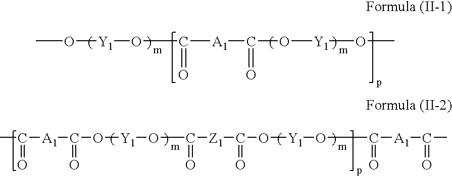
The polymer compound including a repeating unit having, as its partial structure, at least one selected from the formulae (I-1) and (I-2) is not particularly limited, and is preferably a polyester represented by the following formula (II-1) or (II-2):
Figure US07166859-20070123-C01231
In the formulae (II-1) and (II-2), A1 represents at least one selected from the structures represented by the formulae (I-1) and (I-2); Y1 represents a bivalent alcohol residue; Z1 represents a bivalent carboxyl acid residue; m is an integer from 1 to 5; and p is an integer from 5 to 5000.
Specific examples of Y1 or Z1 include groups represented by the following formulae (35) to (40):
Figure US07166859-20070123-C01232
In the formulae (35) to (40), R18 and R19 each represent a hydrogen atom, an alkyl group having 1 to 4 carbon atoms, an alkoxy group having 1 to 4 carbon atoms, a substituted or unsubstituted phenyl group, a substituted or unsubstituted aralkyl group, or a halogen atom; d and e are each an integer from 1 to 10; f is an integer of 0, 1 or 2; h and i are each 0 or 1; V represents a group represented by any one selected from the formulae (14) to (34).
The structure represented by A1 in the formula (II-1) or (II-2) represents at least one selected from structures represented by the formulae (I-1) and (I-2), and may represent two or more selected therefrom if necessary.
The molecular weight (the weight-average molecular weight Mw and the number-average molecular weight Mn) of the polymer compound used in the invention is not particularly limited, and is desirably about 1,000 or more, more desirably from 5,000 to 300,000, when taking into consideration the solubility and thin-film-forming ability of the polymer compound, as well as factors including the affinity of the formed film with a substrate and the flexibility thereof.
For the polymer compound, specific examples of the polyester represented by the formula (II-1) or (II-2) are shown in Tables 102 to 110. However, the polyester used in the invention is not limited thereto.
TABLE 102
Monomer
Compound A1 Ratio Y1 Z1 m p
(1) 2 —CH2CH2 1 18
(2) 5 —CH2CH2 1 41
(3) 9 —CH2CH2 1 32
(4) 9 —CH2CH2
Figure US07166859-20070123-C01233
1 44
(5) 9 —CH2CH2
Figure US07166859-20070123-C01234
1 45
(6) 9 —CH2CH2
Figure US07166859-20070123-C01235
2 85
(7) 13
Figure US07166859-20070123-C01236
1 45
(8) 13
Figure US07166859-20070123-C01237
—(CH2)4 1 30
(9) 19
Figure US07166859-20070123-C01238
1 35
(10) 19 —CH2CH2 1 26
TABLE 103
Monomer
Compound A1 Ratio Y1 Z1 m p
(11) 41 —CH2CH2 1 36
(12) 42 —CH2CH2 1 45
(13) 42 —CH2CH2
Figure US07166859-20070123-C01239
2 56
(14) 39 —CH2CH2 —(CH2)4 1 54
(15) 46 —CH2CH2 1 62
(16) 46 —(CH2)4
Figure US07166859-20070123-C01240
2 22
(17) 49
Figure US07166859-20070123-C01241
1 25
(18) 53
Figure US07166859-20070123-C01242
1 63
(19) 80
Figure US07166859-20070123-C01243
Figure US07166859-20070123-C01244
1 54
(20) 80 —CH2CH2 1 23
TABLE 104
Monomer
Compound A1 Ratio Y1 Z1 m p
(21) 80 —CH2CH2
Figure US07166859-20070123-C01245
1 62
(22) 85
Figure US07166859-20070123-C01246
1 42
(23) 87
Figure US07166859-20070123-C01247
1 26
(24) 87
Figure US07166859-20070123-C01248
Figure US07166859-20070123-C01249
1 24
(25) 88 —CH2CH2 1 29
(26) 92 —CH2CH2 1 39
(27) 127 —CH2CH2
Figure US07166859-20070123-C01250
1 25
(28) 127
Figure US07166859-20070123-C01251
1 45
TABLE 105
Monomer
Compound A1 Ratio Y1 Z1 m p
(29) 127
Figure US07166859-20070123-C01252
1 36
(30) 137
Figure US07166859-20070123-C01253
Figure US07166859-20070123-C01254
1 56
(31) 156 —CH2CH2 1 15
(32) 160 —CH2CH2
Figure US07166859-20070123-C01255
1 35
(33) 173 —CH2CH2 1 34
(34) 175 —CH2CH2 1 16
(35) 178 —CH2CH2 1 35
(36) 181 —CH2CH2 1 56
(37) 182 —CH2CH2 1 53
(38) 183 —CH2CH2 1 26
(39) 191 —CH2CH2 1 45
TABLE 106
Monomer
Compound A1 Ratio Y1 Z1 m p
(40) 193 —CH2CH2 1 36
(41) 233 —CH2CH2 1 55
(42) 234 —CH2CH2 1 36
(43) 238 —CH2CH2 1 63
(44) 243 —CH2CH2
Figure US07166859-20070123-C01256
1 25
(45) 243 —(CH2)4 —(CH2)4 1 45
(46) 243
Figure US07166859-20070123-C01257
1 26
(47) 243 —CH2CH2 1 36
(48) 243 —CH2CH2
Figure US07166859-20070123-C01258
1 46
(49) 248
Figure US07166859-20070123-C01259
1 56
TABLE 107
Monomer
Compound A1 Ratio Y1 Z1 m p
(50) 249 —CH2CH2 1 66
(51) 251 —CH2CH2 1 65
(52) 251
Figure US07166859-20070123-C01260
1 52
(53) 255
Figure US07166859-20070123-C01261
1 15
(54) 262 —CH2CH2 1 45
(55) 267 —CH2CH2
Figure US07166859-20070123-C01262
1 35
(56) 304
Figure US07166859-20070123-C01263
1 26
(57) 306
Figure US07166859-20070123-C01264
1 36
TABLE 108
Monomer
Compound A1 Ratio Y1 Z1 m p
(58) 304
Figure US07166859-20070123-C01265
Figure US07166859-20070123-C01266
1 45
(59) 267 —CH2CH2 1 15
(60) 335 —CH2CH2
Figure US07166859-20070123-C01267
1 65
(61) 335
Figure US07166859-20070123-C01268
1 33
(62) 335
Figure US07166859-20070123-C01269
1 63
(63) 351
Figure US07166859-20070123-C01270
Figure US07166859-20070123-C01271
1 52
(64) 351
Figure US07166859-20070123-C01272
1 45
TABLE 109
Monomer
Compound A1 Ratio Y1 Z1 m p
(65) 375
Figure US07166859-20070123-C01273
1 15
(66) 375
Figure US07166859-20070123-C01274
1 26
(67) 378 —CH2CH2 1 56
(68) 378 —CH2CH2
Figure US07166859-20070123-C01275
1 36
(69) 7/92 1/1 —CH2CH2 1 56
(70) 7/92 1/1 —CH2CH2 2 45
(71) 7/92 1/1
Figure US07166859-20070123-C01276
Figure US07166859-20070123-C01277
1 54
(72) 7/92 1/1 —CH2CH2 1 65
TABLE 110
Com- Monomer
pound A1 Ratio Y1 Z1 m p
(73) 7/127 1/1 —CH2CH2 1 56
(74) 7/127 1/1 —CH2CH2 2 25
(75) 7/175 1/1 —CH2CH2 1 12
(76) 7/92/ 1/1/1 —CH2CH2 1 15
175
(77) 173/ 1/1 —CH2CH2 1 32
220
(78) 7/310 1/1 —CH2CH2
Figure US07166859-20070123-C01278
1 25
(79) 7/310 1/2 —CH2CH2 1 12
(80) 310/ 2/1 —CH2CH2 1 40
337
The numbers in the column “A1” in the column “Monomer” in Tables 102 to 110 correspond to compound numbers described in the column “Structure” in Tables 1 to 101. (The compounds specified by the numbers are specific examples of the compounds represented by the formulae (I-1) and (I-2).) The character “m” represents m in the formulae (II-1) and (II-2).
The process for synthesizing the polymer compound used in the invention is not particularly limited, and may be a process involving a combination of known processes according to the desired structure of the polymer compound. A specific example thereof will now be described using a case in which the polymer compound is a polyester as represented by the formula (II-1) or (II-2). The polymer compound includes a repeating unit having, as its partial structure, at least one selected from the structures represented by the formulae (I-1) and (I-2).
The aromatic tertiary amine used in the invention can be easily synthesized by a process [1] of causing an aryl amine to react with a halogenated carboalkoxyalkylbenzene or a halogenated carboalkoxybenzene to synthesize a diarylamine, and then causing this diarylamine to react with benzidine bishalide or the like. It can otherwise be synthesized by a different process [2] of causing an arylamine, diarylbenzidine or the like to react with a halogenated carboalkoxyalkylbenzene or a halogenated carboalkoxybenzene.
The aromatic tertiary amine having an alkylenecarboxylic acid ester group, which is a monomer used for obtaining a polyester as the polymer compound, can be synthesized by the process described in, for example, JP-A No. 5-80550. That is, by a process of introducing a chloromethyl group, forming a Grignard reagent by use of Mg, converting the chloromethyl group to a carboxylic acid by use of carbon dioxide, and then esterifying the acid.
However, in using this process, a chloromethyl group cannot be introduced into the raw material first used in the initial stage of the series of synthesis reactions in the process since the chloromethyl group has high reactivity. It is therefore necessary to use, for example, one of the three following processes. One process involves forming a skeleton of triarylamine, tetraarylbenzidine, or the like, and, for example, subsequently converting a methyl group, which has been introduced into the raw material first used in the initial stage of the series of synthesis reactions, to a chloromethyl group. A different process involves using an unsubstituted raw material to form a tetraarylbenzidine skeleton, introducing a functional group such as a formyl group into the skeleton to the aromatic ring thereof through a substitution reaction, reducing the group to obtain an alcohol, and then using a halogenation reagent such as thionyl chloride to convert the alcohol group to a chloromethyl group. A further different process involves performing direct chloromethylation with reagents such as para-formaldehyde and hydrochloric acid.
However, any aromatic tertiary amine having a skeleton such as triarylamine or tetraarylbenzidine has very high reactivity. Therefore, according to the process of converting a methyl group to a chloromethyl group, the methyl group having been introduced into the raw material first used in the initial stage of the series of synthesis reactions, a substitution reaction where halogen is introduced to the aromatic ring is easily caused; therefore, it is substantially impossible to selectively chlorinate only the methyl group.
According to the above process of using an unsubstituted raw material by which a functional group such as a formyl group is introduced to the skeleton and subsequently converted into a chloromethyl group, or the above process of performing direct chloromethylation, the chloromethyl group can only be introduced into the para-position to the nitrogen atom. Accordingly, an alkylenecarboxylic acid ester group can also only be introduced to the para-position to the nitrogen atom. Furthermore, reaction steps requires much time to complete in the former process involving the introduction of a functional group and then a chloromethyl group.
On the other hand, the process of causing an arylamine, diarylbenzidine or the like to react with a halogenated carboalkoxyalkylbenzene to yield a monomer is excellent in that the position of a substituent can easily be changed and the ionization potential and other properties of the resultant monomer can be easily controlled. Consequently, physical properties of the polymer compound to be yielded can be controlled. It is possible to easily introduce any of various substituents to an arbitrary position of the aromatic tertiary amine obtained using this kind of synthesis process. Furthermore, the amine is chemically stable, and is easy to handle. Thus, the above-mentioned problems are overcome.
In the case where the polymer compound used in the invention is a polyester as represented by the formula (II-1) or (II-2), the polymer compound can be synthesized by polymerizing a monomer represented by the following formula (II-3), which is obtained by the above synthesis process, in a known manner described, for example, in Experimental Chemical Lecture (Jikken Kagaku Kouza) vol. 28, 4th ed. (Maruzen Co., Ltd., 1992).
A′-A1-A′  Formula (II-3)
In the formula (II-3), A1 represents at least one selected from the structures represented by the formulae (I-1) and (I-2); A′ represents a hydroxyl group, a halogen atom, or —O—R20 wherein R20 represents an alkyl group, a substituted or unsubstituted aryl group, or an aralkyl group.
Specifically, a polyester represented by the formula (II-1) or (II-2) can be synthesized as follows.
1) In the case where A′ is a hydroxyl group, a bivalent alcohol is mixed with a monomer in an amount substantially equivalent to the monomer, after which the two are polymerized with an acidic catalyst. The bivalent alcohol is represented by OH—(Y1—O)m-H wherein Y1 has the same meaning as described above and m is an integer equal to or greater than 1. The acidic catalyst may be an acidic catalyst which is used in ordinary esterifying reactions, examples of which include sulfuric acid, toluenesulfonic acid, and trifluoroacetic acid. The amount of the catalyst is from 1/10,000 to 1/10 parts by mass, preferably from 1/1,000 to 1/50 parts by mass, per 1 part by mass of the monomer.
To remove water generated in the polymerization, it is preferable to use a solvent that is azeotropic with water. Examples of effective solvents include toluene, chlorobenzene, and 1-chloronaphthalene. The amount of the solvent is from 1 to 100 parts by mass, preferably from 2 to 50 parts by mass, per 1 part by mass of the monomer. The reaction temperature can be arbitrarily set, and is preferably made to be equal to the boiling point of the solvent in order to remove water generated in the polymerization.
After the completion of the reaction, when the solvent is not used, the reaction product is dissolved in a solvent able to dissolve the reaction product. When the solvent is used, the reaction solution is dripped, as it is, in to a poor solvent wherein a polymer to be obtained does not easily dissolve, for example, an alcohol (such as methanol or ethanol), or acetone, so as to precipitate a polyester. The polyester is separated, washed sufficiently with water or an organic solvent, and then dried. Furthermore, if necessary, the resultant product may be repeatedly subjected to reprecipitation treatment where the product is dissolved in an appropriate organic solvent and the solution is dripped into a poor solvent to precipitate the polyester.
In the reprecipitation treatment, it is preferable that the solution be effectively stirred with a mechanical stirrer or the like. The amount of solvent for dissolving the polyester in the reprecipitation treatment is from 1 to 100 parts by mass, preferably from 2 to 50 parts by mass, per 1 part by mass of the polyester. The amount of the poor solvent is from 1 to 1,000 parts by mass, preferably from 10 to 500 parts by mass, per 1 part by mass of the polyester. 2) In the case that A′ is halogen, a bivalent alcohol represented by OH—(Y1—O)m-H is mixed with the monomer, in an amount substantially equivalent to the monomer, and then the two are polymerized with an organic basic catalyst such as pyridine or triethylamine. The amount of the organic basic catalyst is from 1 to 10 equivalents, preferably from 2 to 5 equivalents, per 1 equivalent of the monomer.
A solvent may be used, and examples of effective solvents include methylene chloride, tetrahydrofuran (THF), toluene, and chlorobenzene, and 1-chloronaphthalene. The amount of the solvent is from 1 to 100 parts by mass, preferably from 2 to 50 parts by mass, per 1 part by mass of the monomer. The reaction temperature can be arbitrarily set. After polymerization, reprecipitation treatment is conducted as described above to purify the resultant polymer.
In the case where the above-mentioned bivalent alcohol is a bivalent alcohol having a high acidity, such as bisphenol, interfacial polymerization may be used. In other words, the bivalent alcohol is added to water, a base is added thereto in an amount equivalent to the bivalent alcohol, and the mixture is dissolved. Then a solution of the monomer, the amount of which being equivalent to the bivalent alcohol, is added to the alcohol solution while the alcohol solution is stirred vigorously, whereby the alcohol and the monomer are polymerized. At this time, the amount of water is from 1 to 1,000 parts by mass, preferably from 2 to 500 parts by mass, per 1 part by mass of the bivalent alcohol.
Examples of the effective solvents for dissolving the monomer include methylene chloride, dichloroethane, trichloroethane, toluene, chlorobenzene, and 1-chloronaphthalene. The reaction temperature can be arbitrarily set. In order to promote the reaction, it is effective to use a phase transfer catalyst such as an ammonium salt or a sulfonium salt. The amount of the phase transfer catalyst is from 0.1 to 10 parts by mass, preferably from 0.2 to 5 parts by mass, per 1 part by mass of the monomer.
3) In the case where A′ is —O—R20, a bivalent alcohol represented by OH—(Y1—O)m-H is excessively added to a monomer after which the resultant solution is heated in the presence of an inorganic acid (such as sulfuric acid or phosphoric acid), titanium alkoxide, an acetate or carbonate of calcium, cobalt or the like, or an oxide of zinc or lead so as to perform transesterification and thereby synthesize the above-mentioned polyester.
The amount of the bivalent alcohol is from 2 to 100 equivalents, preferably from 3 to 50 equivalents, per 1 equivalent of the monomer. The amount of the catalyst is from 1/10,000 to 1 part by mass, preferably from 1/1,000 to 1/2 parts by mass, per 1 part by mass of the monomer. The reaction is conducted at a reaction temperature of 200 to 300° C. It is preferable to carry out the reaction under reduced pressure in order to promote polymerization through the release of OH—(Y1—O)m-H after the completion of the transesterification from the group —O—R20 to the group —O—(Y1—O)m-H. The reaction may be carried out while a high boiling point solvent which is azeotropic with OH—(Y1—O)m-H, such as 1-chloronaphthalane, is used to remove OH—(Y1—O)m-H at normal pressure by azeotropy.
The polyester can be synthesized as follows. In each of the above-mentioned cases, the reaction is advanced by the addition of an excessive amount of the bivalent alcohol, thereby producing a compound represented by the following formula (II-4). The compound is next used instead of the monomer represented by the formula (II-3) to react with a bivalent carboxylic acid, a bivalent carboxylic acid halide or the like in the same manner as described above. The polyester can thus be obtained.
Figure US07166859-20070123-C01279
In the formula (II-4), Al represents at least one selected from the structures represented by the formulae (I-1) and (I-2); Y1 represents a bivalent alcohol residue; and m is an integer from 1 to 5.
The structure of the organic semiconductor transistor element according to the invention will now be described in detail with specific examples thereof.
The organic semiconductor transistor element according to the invention has a structure that includes a source electrode, a drain electrode, an organic semiconductor formed to be electrically conductive to the source electrode and the drain electrode, and a gate electrode which is both insulated from the organic semiconductor and capable of applying an electric field. The organic semiconductor includes the above-mentioned polymer compound, which contains an aromatic tertiary amine. The organic semiconductor transistor element according to the invention can be made in any desired shape as the case may be, and is preferably made in the form of a thin film.
The structure of the organic semiconductor transistor element according to the invention will now be described in more detail with reference to the attached drawings. However, the organic semiconductor transistor element according to the invention is not limited thereto.
FIGS. 1 to 3 are each a schematic sectional view showing individual examples of the structure of the organic semiconductor transistor element of the invention. The organic semiconductor transistor elements according to the invention shown in FIGS. 1 and 2 each have a field effect transistor structure. The organic semiconductor transistor element according to the invention illustrated in FIG. 3 has a static induction transistor structure.
In FIGS. 1 to 3, the same reference numbers are used to indicate members having a common function. Reference number 1 represents a substrate; 2, a source electrode; 3, a drain electrode; 4, an organic semiconductor layer; 5, a gate electrode or gate electrodes; and 6, an insulating layer. The structures of the organic semiconductor transistor elements of the present invention shown in FIGS. 1 to 3 are described individually hereinafter.
In the organic semiconductor transistor element according to the invention shown in FIG. 1, the gate electrode 5 and the insulating layer 6 are formed, in that order, on the substrate 1, and the source electrode 2 and the drain electrode 3 are formed on the insulating layer 6 so as to be located away from each other. The organic semiconductor layer 4 is formed so as to cover the source electrode 2 and the drain electrode 3.
In the organic semiconductor transistor element according to the invention illustrated in FIG. 2, the gate electrode 5 and the insulating layer 6 are formed, in that order, on the substrate 1. The source electrode 2 is formed on the insulating layer 6, and the organic semiconductor layer 4 is formed on the insulating layer 6 so as to cover a surface of the source electrode 2 opposite to another surface thereof which is in contact with the insulating layer 6. Furthermore, the drain electrode 3 is formed on a surface of the organic semiconductor layer 4 opposite to another surface thereof which is in contact with the insulating layer 6, so as to be located away from the source electrode 2 in the direction of the plane of the substrate 1.
In the organic semiconductor transistor element according to the invention shown in FIG. 3, the source electrode 2, the organic semiconductor layer 4, and the drain electrode 3 are formed, in that order, on the substrate 1. The gate electrodes 5 are formed inside the organic semiconductor layer 4. (In this example, the gate electrodes 5 are four in number, and are arranged at regular intervals parallel to the direction of the plane of the substrate 1.)
The gate electrodes 5 are arranged perpendicularly to the surface of the drawing sheet and parallel to both the source electrode 2 and the drain electrode 3, and further are arranged in parallel to each other. In FIG. 3, the gate electrodes 5 are electrically insulated from the organic semiconductor layer 4 with an insulating layer (not shown) formed therebetween.
In the organic semiconductor transistor elements as shown in FIGS. 1 to 3, electric current flowing between the source electrode 2 and the drain electrode 3 can be controlled through voltage applied to the gate electrode(s) 5.
In producing an electronic device having a semiconductor device, a structure having one or more organic semiconductor transistor elements according to the invention mounted on a substrate can be used as the semiconductor device. Other components, circuits, etc. are combinable with the semiconductor device to produce an electronic device.
Each of the members which constitute the organic semiconductor element or the semiconductor device according to the present invention except the organic semiconductor part thereof will now be described in detail.
Electrode material used in the source electrode, the drain electrode and the gate electrode may be any material capable of injecting electric charge effectively, and specific examples thereof include metal, metal oxide, and electroconductive polymer.
Examples of metals include magnesium, aluminum, gold, silver, copper, chromium, tantalum, indium, palladium, lithium, calcium, and alloys thereof. Examples of metal oxides include lithium oxide, magnesium oxide, aluminum oxide, indium tin oxide (ITO), tin oxide (NESA), indium oxide, zinc oxide, and indium zinc oxide.
Examples of electroconductive polymers include polyaniline, polythiophene, polythiophene derivatives, polypyrrole, polypyridine, and complexes of polyethylenedioxythiophene and polystyrenesulfonic acid.
If the difference between the ionization potential of the electrode material and that of the above-mentioned polymer compound used in the organic semiconductor (layer) is large, the charge injecting property of the electrode or device is adversely affected. Therefore, the difference between the ionization potential of the material used in the drain electrode and/or the source electrode and that of the polymer compound used in the organic semiconductor (layer) is preferably about 1.0 eV or less, more preferably 0.5 eV or less. For the electrode material, Au is particularly preferable from the viewpoint of the difference in ionization potential between the electrode(s) and the polymer compound.
One of the following three methods can be used for producing each of the electrodes: a method involving making a thin film formed from the above-mentioned electrode material by a known thin-film-forming process, such as vapor deposition or sputtering, into a desired shape by a known photolithography or lift-off process; a different method involving etching the thin film into a desired pattern (electrode shape) by use of a resist formed by ink-jet printing or the like; or a further different method involving transferring the electrode material, such as aluminum, thermally and directly. In the case where the above-mentioned electroconductive polymer is used as the electrode material, the polymer can be dissolved in a solvent, after which the resultant solution can be patterned by ink-jet printing.
Examples of the insulating material for insulating the electrodes from each other or insulating the gate electrode(s) from the organic semiconductor (layer) include inorganic substances such as silicon dioxide, silicon nitride, tantalum oxide, aluminum oxide, and titanium oxide; and organic insulating polymers such as polycarbonate resin, polyester resin, methacrylic resin, acrylic resin, polyvinyl chloride resin, cellulose resin, urethane resin, epoxy resin, polystyrene resin, polyvinyl acetate resin, styrene-butadiene copolymer, vinylidene chloride-acrylonitrile copolymer, vinyl chloride-vinyl acetate-maleic anhydride copolymer, and silicone resin. However, the insulating material is not limited thereto.
Examples of the substrate include a substrate being made of silicon monocrystal doped with phosphorus in a high concentration; a glass substrate; and a plastic substrate made of polycarbonate resin, polyester resin, methacrylic resin, acrylic resin, polyvinyl chloride resin, cellulose resin, urethane resin, epoxy resin, polystyrene resin, polyvinyl acetate resin, styrene-butadiene copolymer, vinylidene chloride-acrylonitrile copolymer, vinyl chloride-vinyl acetate-maleic anhydride copolymer, or silicone resin. However, the substrate is not limited thereto.
In particular, when the organic semiconductor transistor element according to the invention is used in an electronic circuit of an electronic device required to have flexibility, such as electronic paper or digital paper, (hereinafter referred to as a “flexible electronic device”), it is desirable that a flexible substrate be used for the substrate thereof. In particular, by using a substrate having a flexural modulus of about 1000 MPa or more, preferably 5000 MPa or more, the organic semiconductor transistor element according to the invention can be adapted to a driving circuit or electronic circuit of a display element having flexiblity.
The organic semiconductor transistor element according to the invention has sufficient elasticity for such an application since the organic semiconductor part of the element contains the above-mentioned polymer compound as the main component thereof; thus, even if the element is formed on the flexible substrate, the element resists any great deformation or repeated deformation and the element is thereby able to maintain stabilized performance. In contract, the semiconductor part of an inorganic semiconductor transistor element is made of an inorganic substance, and the transistor element thus lacks elasticity. Therefore, it is very difficult to use this kind of transistor element for purposes in which, it is subjected to the kind of deformation described above. Furthermore, an inorganic semiconductor transistor element has the disadvantage that no plastic can be used as the material of the substrate thereof since the transistor element is required to undergo high temperatures during the production process. Likewise, an organic semiconductor transistor element having an organic semiconductor part made mainly of a low molecular weight material lacks elasticity, unlike polymer material. Therefore, it is also difficult to use a transistor element of this nature for application where it is subjected to deformation as described above; alternatively, such use of this kind of transistor element results in unreliability.
In the present invention, “flexible electronic device” means an electronic device satisfying each of the following conditions [1] to [3]: [1] the device can be used while being altered from a flat state to a bent, warped or wound state, or vice versa, regardless of whether the power supply thereto is cut or not, as can be performed with the above-mentioned electronic paper or digital paper; [2] the device has a structure comprising a substrate, and one or more organic semiconductor transistor elements, and [3] the substrate of the device on which the organic semiconductor transistor element(s) is/are formed is required to have the flexibility described in condition [1].
A liquid-phase film-forming method is preferably used for forming the organic semiconductor part into a layer form. Examples thereof include spin coating, casting, dipping, die coating, roll coating, bar coating, and ink-jet coating, and various printing methods. However, the liquid-phase film-forming method is not limited thereto.
A protective layer may be formed on the organic semiconductor transistor element to prevent the element from being deteriorated by moisture or oxygen. Specific examples of material for the protective layer include metals such as In, Sn, Pb, Au, Cu, Ag and Al; metal oxides such as MgO, SiO2 and TiO2; and resins such as polyethylene resin, polyurea resin, and polyimide resin. The protective layer can be formed through vacuum evaporation, sputtering, plasma polymerization, CVD, or coating.
As described above, according to the organic semiconductor transistor element of the invention, the on/off ratio thereof can be adjusted to fall within a range of about 102 to 105 according to the intended purpose of the organic semiconductor transistor element by appropriately selecting, for example, the kind of polymer compound to be used in the organic semiconductor part of the element, and the structure of the element.
EXAMPLES
The present invention is more specifically described hereinafter by way of the following examples. However, the present invention is not limited by these examples.
(Example 1)
Gold is deposited in film form on a glass substrate by vacuum evaporation, forming a gate electrode with a thickness of 100 nm. Next, SiO2 is deposited on the gate electrode by sputtering, so as to form an insulating layer with a thickness of 300 nm. Thereafter, a metal mask is set on the insulating layer and gold is deposited in film form on the insulating layer, so as to form a source electrode and a drain electrode each with a thickness of 150 nm. The distance between the two formed electrodes is 50 μm.
To form an organic semiconductor layer, a 5% by mass solution of the example compound (6) in dichloroethane is prepared, and this is filtrated through a PTFE filter having sieve openings of 0.1 μm to prepare a coating solution.
The coating solution is then used to form an organic semiconductor layer with a thickness of 0.150 μm on the insulating layer by dip coating, so as to cover the source electrode and the drain electrode.
(Example 2)
An organic semiconductor transistor element is produced in the same way as in Example 1 except that the exempla compound (8) is used instead of the exempla compound (6) used in Example 1.
(Example 3)
An organic semiconductor transistor element is produced in the same way as in Example 1 except that the exempla compound (20) is used instead of the exempla compound (6) used in Example 1.
(Example 4)
An organic semiconductor transistor element is produced in the same way as in Example 1 except that the exemplified compound (37) is used instead of the exempla compound (6) used in Example 1.
(Example 5)
An organic semiconductor transistor element is produced in the same way as in Example 1 except that the exempla compound (39) is used instead of the exempla compound (6) used in Example 1.
(Example 6)
An organic semiconductor transistor element is produced in the same way as in Example 1 except that the exempla compound (47) is used instead of the exempla compound (6) used in Example 1.
(Example 7)
An organic semiconductor transistor element is produced in the same way as in Example 1 except that the exempla compound (67) is used instead of the exempla compound (6) used in Example 1.
(Comparative Example 1)
An organic semiconductor transistor element is produced in the same way as in Example 1 except that a charge-transporting low molecular weight compound represented by the following structural formula (IX) is used instead of the exempla compound (6) used in Example 1.
Figure US07166859-20070123-C01280
(Comparative Example 2)
An organic semiconductor transistor element is produced in the same way as in Example 1 except that poly[2-methoxy-5-(2-ethylhexyl)-1,4-phenylenevinylene] is used instead of the exempla compound (6) used in Example 1.
-Evaluation-
A semiconductor parameter analyzer (trade name: 4155C, manufactured by Agilent Technologies Co.) is used to measure the current-voltage characteristic of each of the organic semiconductor transistor elements obtained in the working examples according to the invention and the comparative examples when gate voltage is applied thereto. The carrier mobilities (linear region) and the on/off ratios thereof are then calculated.
The on/off ratios of the organic semiconductor transistor elements produced as described above are shown in Table 111 together with the carrier mobilities of charge-transporting materials used in their organic compound layers. As can be understood from Table 111, the organic semiconductor transistor element in any one of the working examples exhibits a switching property where the drain-source current flowing between the source electrode and the drain electrode through the organic semiconductor layer changes with a change in voltage applied to the gate electrode (gate voltage), and the on/off ratio thereof is in the order of 104.
In contract, in each of the comparative examples, the carrier mobility of the charge-transporting material used in the formation of the organic semiconductor layer is low. Accordingly, there are cases where the on/off ratio thereof is far poorer than the ratios of the working examples, and there are also cases in which a liquid-phase film-forming process cannot be used, and thus, a gas-phase film-forming process must be used in order to form the organic semiconductor layer.
TABLE 111
Carrier mobility On/off ratio
Example 1 (cm2/Vs) (×102)
Example 2 3.7 × 10⁻⁴ 42
Example 3 2.1 × 10⁻⁵ 62
Example 4 6.7 × 10⁻⁵ 26
Example 5 8.5 × 10⁻⁶ 55
Example 6 4.5 × 10⁻⁵ 10
Example 7 1.5 × 10⁻⁶ 41
Example 8 2.4 × 10⁻⁶ 25
Comparative Example 1 2.7 × 10⁻⁷ 0.27
Comparative Example 2 1.0 × 10⁻⁶ 10
As described above, according to the invention, a polymer compound is used which contains an aromatic tertiary amine having excellent solubility in solvent or resin, excellent compatibility with solvent or resin, and a high carrier mobility. The present invention therefore makes it possible to provide an organic semiconductor transistor element which has a high operating speed and is easy to produce, a semiconductor device using this element, and a process for producing the semiconductor device.

Claims (20)

1. An organic semiconductor transistor element, comprising at least a source electrode, a drain electrode, an organic semiconductor formed to be electrically conductive to the source electrode and the drain electrode, and a gate electrode which is both insulated from the organic semiconductor and capable of applying an electric field,
wherein the organic semiconductor comprises a polymer compound comprising an aromatic tertiary amine.
2. An organic semiconductor transistor element according to claim 1, wherein the polymer compound is a polyester.
3. An organic semiconductor transistor element according to claim 1, wherein the molecular weight of the polymer compound is about 1000 or more.
4. An organic semiconductor transistor element according to claim 1, wherein the aromatic tertiary amine contains an aromatic component comprising at least one of a condensed aromatic ring and a polynuclear aromatic ring, bonded to a tertiary amine nitrogen atom thereof.
5. An organic semiconductor transistor element according to claim 1, wherein the aromatic tertiary amine is represented by one of the following formulae (I-1) and (I-2):
Figure US07166859-20070123-C01281
wherein Ar represents one selected from the group consisting of a substituted or unsubstituted monovalent benzene ring, a substituted or unsubstituted monovalent polynuclear aromatic hydrocarbon having 2 to 10 aromatic rings, a substituted or unsubstituted monovalent condensed aromatic hydrocarbon having 2 to 10 aromatic rings, and a substituted or unsubstituted monovalent aromatic heteroring; X represents one selected from the group consisting of a substituted or unsubstituted bivalent benzene ring, a substituted or unsubstituted bivalent polynuclear aromatic hydrocarbon having 2 to 10 aromatic rings, a substituted or unsubstituted bivalent condensed aromatic hydrocarbon having 2 to 10 aromatic rings, and a substituted or unsubstituted bivalent aromatic heteroring; T represents one selected from the group consisting of a bivalent straight-chain hydrocarbon group having 1 to 6 carbon atoms, and a bivalent branched hydrocarbon group having 2 to 10 carbon atoms; and k, i, and j each independently represent an integer which is one of 0 and 1.
6. An organic semiconductor transistor element according to claim 5, wherein the polymer compound is a polyester represented by one of the following formulae (II-1) and (II-2):
Figure US07166859-20070123-C01282
wherein A1 represents at least one aromatic tertiary amine selected from the structures represented by the formulae (I-1) and (I-2); Y1 represents a bivalent alcohol residue; Z1 represents a bivalent carboxylic acid residue; m represents an integer from 1 to 5; and p represents an integer from 5 to 5000.
7. An organic semiconductor transistor element according to claim 1, wherein the difference between an ionization potential of one of the source electrode and the drain electrode and that of the polymer compound is about 1.0 eV or less.
8. A semiconductor device, comprising a substrate, and one or more organic semiconductor transistor elements provided on the substrate,
the one or more organic semiconductor transistor elements comprising at least a source electrode, a drain electrode, an organic semiconductor formed to be electrically conductive to the source electrode and the drain electrode, and a gate electrode which is both insulated from the organic semiconductor and capable of applying an electric field,
wherein the organic semiconductor comprises a polymer compound comprising an aromatic tertiary amine.
9. A semiconductor device according to claim 8, wherein the flexural modulus of the substrate is about 1000 MPa or more.
10. A semiconductor device according to claim 9, which is used in a flexible electronic device.
11. A semiconductor device according to claim 8, wherein the polymer compound is a polyester.
12. A semiconductor device according to claim 8, wherein the molecular weight of the polymer compound is about 1000 or more.
13. A semiconductor device according to claim 8, wherein the aromatic tertiary amine contains an aromatic component comprising at least one of a condensed aromatic ring and a polynuclear aromatic ring, bonded to a tertiary amine nitrogen atom thereof.
14. A semiconductor device according to claim 8, wherein the aromatic tertiary amine is represented by one of the following formulae (I-1) and (I-2):
Figure US07166859-20070123-C01283
wherein Ar represents one selected from the group consisting of a substituted or unsubstituted monovalent benzene ring, a substituted or unsubstituted monovalent polynuclear aromatic hydrocarbon having 2 to 10 aromatic rings, a substituted or unsubstituted monovalent condensed aromatic hydrocarbon having 2 to 10 aromatic rings, and a substituted or unsubstituted monovalent aromatic heteroring; X represents one selected from the group consisting of a substituted or unsubstituted bivalent benzene ring, a substituted or unsubstituted bivalent polynuclear aromatic hydrocarbon having 2 to 10 aromatic rings, a substituted or unsubstituted bivalent condensed aromatic hydrocarbon having 2 to 10 aromatic rings, and a substituted or unsubstituted bivalent aromatic heteroring; T represents one selected from the group consisting of a bivalent straight-chain hydrocarbon group having 1 to 6 carbon atoms, and a bivalent branched hydrocarbon group having 2 to 10 carbon atoms; and k, i, and j each independently represent an integer which is one of 0 and 1.
15. A semiconductor device according to claim 14, wherein the polymer compound is a polyester represented by one of the following formulae (II-1) and (II-2):
Figure US07166859-20070123-C01284
wherein A1 represents at least one aromatic tertiary amine selected from the structures represented by the formulae (I-1) and (I-2); Y1 represents a bivalent alcohol residue; Z1 represents a bivalent carboxylic acid residue; m represents an integer from 1 to 5; and p represents an integer from 5 to 5000.
16. A semiconductor device according to claim 8, wherein the difference between an ionization potential of one of the source electrode and the drain electrode and that of the polymer compound is about 1.0 eV or less.
17. A process for producing a semiconductor device comprising a substrate, and one or more organic semiconductor transistor elements provided on the substrate,
the one or more organic semiconductor transistor elements comprising at least a source electrode, a drain electrode, an organic semiconductor layer which is formed to be electrically conductive to the source electrode and the drain electrode and which comprises a polymer compound comprising an aromatic tertiary amine, and a gate electrode which is both insulated from the organic semiconductor layer and capable of applying an electric field,
wherein the organic semiconductor layer is formed through a liquid-phase film-forming process.
18. A process for producing a semiconductor device according to claim 17, wherein the polymer compound is a polyester.
19. A process for producing a semiconductor device according to claim 17, wherein the molecular weight of the polymer compound is about 1000 or more.
20. A process for producing a semiconductor device according to claim 17, wherein the flexural modulus of the substrate is about 1000 MPa or more.
US10/959,224 2003-11-17 2004-10-07 Organic semiconductor transistor element, semiconductor device using the same, and process for producing the semiconductor device Expired - Fee Related US7166859B2 (en)

Applications Claiming Priority (2)

Application Number Priority Date Filing Date Title
JP2003-386590 2003-11-17
JP2003386590 2003-11-17

Publications (2)

Publication Number Publication Date
US20050104097A1 US20050104097A1 (en) 2005-05-19
US7166859B2 true US7166859B2 (en) 2007-01-23

Family

ID=34567415

Family Applications (1)

Application Number Title Priority Date Filing Date
US10/959,224 Expired - Fee Related US7166859B2 (en) 2003-11-17 2004-10-07 Organic semiconductor transistor element, semiconductor device using the same, and process for producing the semiconductor device

Country Status (3)

Country Link
US (1) US7166859B2 (en)
KR (1) KR100692448B1 (en)
CN (1) CN100428521C (en)

Cited By (8)

* Cited by examiner, † Cited by third party
Publication number Priority date Publication date Assignee Title
US20060192199A1 (en) * 2005-02-25 2006-08-31 Xerox Corporation Celluloses and devices thereof
US20070045618A1 (en) * 2005-08-24 2007-03-01 Sanyo Electric Co., Ltd. Organic semiconductor material, organic semiconductor element and field effect transistor using the same
US20070292681A1 (en) * 2006-06-20 2007-12-20 Fuji Xerox Co., Ltd Organic electroluminescence device
US20080067505A1 (en) * 2006-09-15 2008-03-20 Samsung Electronics Co., Ltd. Composition for preparing organic insulating film, organic insulating film prepared by using the same and organic thin film transistor comprising the organic insulating film
US20080197345A1 (en) * 2007-02-16 2008-08-21 Samsung Electronics Co., Ltd Copolymer, organic insulating layer composition, and organic insulating layer and organic thin film transistor manufactured using the same
US20080306239A1 (en) * 2007-06-07 2008-12-11 Fuji Xerox Co., Ltd. Quinoxaline-containing compounds and polymers thereof
US20090039774A1 (en) * 2007-08-07 2009-02-12 Fuji Xerox Co., Ltd. Organic electroluminescence element and display device
US20090075439A1 (en) * 2006-01-31 2009-03-19 International Business Machines Corporation Microelectronic structure by selective deposition

Families Citing this family (5)

* Cited by examiner, † Cited by third party
Publication number Priority date Publication date Assignee Title
US20070075308A1 (en) * 2005-09-30 2007-04-05 Florian Dotz Active semiconductor devices
KR100647712B1 (en) * 2005-11-09 2006-11-23 삼성에스디아이 주식회사 Organic light emitting display device
KR101363714B1 (en) * 2006-12-11 2014-02-14 엘지디스플레이 주식회사 Organic thin film transistor, manufacturing method thereof, electrostatic discharge device using the same, liquid crystal display device and manufacturing method thereof
TWI377713B (en) 2007-10-19 2012-11-21 Ind Tech Res Inst Stacked structure and method of patterning the same and organic thin film transistor and array including the same
TW201605053A (en) * 2014-07-22 2016-02-01 中華映管股份有限公司 Thin film transistor

Citations (13)

* Cited by examiner, † Cited by third party
Publication number Priority date Publication date Assignee Title
JPH0555568A (en) 1991-08-28 1993-03-05 Asahi Chem Ind Co Ltd Thin organic film transistor
JPH05190877A (en) 1991-11-29 1993-07-30 Matsushita Giken Kk Manufacture of diode element
JPH08228034A (en) 1994-12-09 1996-09-03 At & T Corp Organic thin film transistor device
JPH08228035A (en) 1994-12-09 1996-09-03 At & T Corp Thin film transistor device and manufacture thereof
JPH08264805A (en) 1995-03-02 1996-10-11 At & T Ipm Corp Product containing alpha-hexaphenyl
JPH10125924A (en) 1996-10-17 1998-05-15 Matsushita Electric Ind Co Ltd Org. thin film transistor, liq. crystal element and org. light emitting element
JPH10190001A (en) 1996-12-20 1998-07-21 Lucent Technol Inc Manufacture of organic thin film transistor
JPH10270712A (en) 1997-03-25 1998-10-09 Internatl Business Mach Corp <Ibm> Structure of thin film transistor device
JP2000174277A (en) 1998-12-01 2000-06-23 Hitachi Ltd Thin film transistor and its manufacture
US6096822A (en) * 1998-04-21 2000-08-01 Alliedsignal Inc. Low molecular weight polyester or polyamide pigment dispersing composition and color concentrate for the manufacture of colored polymers
JP2001094107A (en) 1999-09-20 2001-04-06 Hitachi Ltd Organic semiconductor device and liquid crystal display device
US6720644B2 (en) * 2000-10-10 2004-04-13 Sony Corporation Semiconductor device using interposer substrate and manufacturing method therefor
JP2005047810A (en) * 2003-07-29 2005-02-24 Tetsuya Nishio Liquid crystalline compound and liquid crystalline organic semiconductor using the same

Family Cites Families (4)

* Cited by examiner, † Cited by third party
Publication number Priority date Publication date Assignee Title
JP2000030867A (en) * 1992-11-11 2000-01-28 Toppan Printing Co Ltd Organic thin film el element
US5936259A (en) * 1997-10-16 1999-08-10 Lucent Technologies Inc. Thin film transistor and organic semiconductor material thereof
DE10153450A1 (en) * 2001-10-30 2003-05-22 Covion Organic Semiconductors Process for the production of arylamines
CN1144301C (en) * 2002-04-05 2004-03-31 中国科学院长春应用化学研究所 Organic film transistor switch device and making method thereof

Patent Citations (13)

* Cited by examiner, † Cited by third party
Publication number Priority date Publication date Assignee Title
JPH0555568A (en) 1991-08-28 1993-03-05 Asahi Chem Ind Co Ltd Thin organic film transistor
JPH05190877A (en) 1991-11-29 1993-07-30 Matsushita Giken Kk Manufacture of diode element
JPH08228034A (en) 1994-12-09 1996-09-03 At & T Corp Organic thin film transistor device
JPH08228035A (en) 1994-12-09 1996-09-03 At & T Corp Thin film transistor device and manufacture thereof
JPH08264805A (en) 1995-03-02 1996-10-11 At & T Ipm Corp Product containing alpha-hexaphenyl
JPH10125924A (en) 1996-10-17 1998-05-15 Matsushita Electric Ind Co Ltd Org. thin film transistor, liq. crystal element and org. light emitting element
JPH10190001A (en) 1996-12-20 1998-07-21 Lucent Technol Inc Manufacture of organic thin film transistor
JPH10270712A (en) 1997-03-25 1998-10-09 Internatl Business Mach Corp <Ibm> Structure of thin film transistor device
US6096822A (en) * 1998-04-21 2000-08-01 Alliedsignal Inc. Low molecular weight polyester or polyamide pigment dispersing composition and color concentrate for the manufacture of colored polymers
JP2000174277A (en) 1998-12-01 2000-06-23 Hitachi Ltd Thin film transistor and its manufacture
JP2001094107A (en) 1999-09-20 2001-04-06 Hitachi Ltd Organic semiconductor device and liquid crystal display device
US6720644B2 (en) * 2000-10-10 2004-04-13 Sony Corporation Semiconductor device using interposer substrate and manufacturing method therefor
JP2005047810A (en) * 2003-07-29 2005-02-24 Tetsuya Nishio Liquid crystalline compound and liquid crystalline organic semiconductor using the same

Non-Patent Citations (1)

* Cited by examiner, † Cited by third party
Title
C.J. Drury et al.; "Low-Cost All-Polymer Integrated Circuits"; American Institute of Physics; vol. 73, No. 1; Jul. 6, 1998; pp. 108-110.

Cited By (16)

* Cited by examiner, † Cited by third party
Publication number Priority date Publication date Assignee Title
US7619242B2 (en) * 2005-02-25 2009-11-17 Xerox Corporation Celluloses and devices thereof
US20060192199A1 (en) * 2005-02-25 2006-08-31 Xerox Corporation Celluloses and devices thereof
US20070045618A1 (en) * 2005-08-24 2007-03-01 Sanyo Electric Co., Ltd. Organic semiconductor material, organic semiconductor element and field effect transistor using the same
US7781757B2 (en) 2005-08-24 2010-08-24 Sanyo Electric Co., Ltd. Organic semiconductor material, organic semiconductor element and field effect transistor using the same
US8138100B2 (en) * 2006-01-31 2012-03-20 International Business Machines Corporation Microelectronic structure by selective deposition
US20090075439A1 (en) * 2006-01-31 2009-03-19 International Business Machines Corporation Microelectronic structure by selective deposition
US8697561B2 (en) 2006-01-31 2014-04-15 International Business Machines Corporation Microelectronic structure by selective deposition
US20070292681A1 (en) * 2006-06-20 2007-12-20 Fuji Xerox Co., Ltd Organic electroluminescence device
US20080067505A1 (en) * 2006-09-15 2008-03-20 Samsung Electronics Co., Ltd. Composition for preparing organic insulating film, organic insulating film prepared by using the same and organic thin film transistor comprising the organic insulating film
US8273460B2 (en) 2006-09-15 2012-09-25 Samsung Electronics Co., Ltd. Composition for preparing organic insulating film, organic insulating film prepared by using the same and organic thin film transistor comprising the organic insulating film
US20080197345A1 (en) * 2007-02-16 2008-08-21 Samsung Electronics Co., Ltd Copolymer, organic insulating layer composition, and organic insulating layer and organic thin film transistor manufactured using the same
US7675059B2 (en) * 2007-02-16 2010-03-09 Samsung Electronics Co., Ltd. Copolymer, organic insulating layer composition, and organic insulating layer and organic thin film transistor manufactured using the same
US20080306239A1 (en) * 2007-06-07 2008-12-11 Fuji Xerox Co., Ltd. Quinoxaline-containing compounds and polymers thereof
US8102113B2 (en) * 2007-06-07 2012-01-24 Fuji Xerox Co., Ltd. Quinoxaline-containing compounds and polymers thereof
US20090039774A1 (en) * 2007-08-07 2009-02-12 Fuji Xerox Co., Ltd. Organic electroluminescence element and display device
US8264140B2 (en) * 2007-08-07 2012-09-11 Fuji Xerox Co., Ltd. Organic electroluminescence element and display device

Also Published As

Publication number Publication date
KR20050047462A (en) 2005-05-20
CN100428521C (en) 2008-10-22
KR100692448B1 (en) 2007-03-09
US20050104097A1 (en) 2005-05-19
CN1619855A (en) 2005-05-25

Similar Documents

Publication Publication Date Title
US10011684B2 (en) Arylamine polymer, method for producing the same, ink composition, film, electronic device, organic thin-film transistor, and display device
US7498084B2 (en) Macromolecular structure, functional device having the same, transistor, and display apparatus using the same
US7166859B2 (en) Organic semiconductor transistor element, semiconductor device using the same, and process for producing the semiconductor device
US7528261B2 (en) Small molecule compound having indolocarbazole moiety and divalent linkage
JP5307349B2 (en) Functionalized heteroacenes and electronic devices made therefrom
EP2027187B1 (en) Thiazolothiazole derivatives and organic electronic device using the same
US7829727B2 (en) Device containing compound having indolocarbazole moiety and divalent linkage
US7902382B2 (en) Thiophene-containing compound and thiophene-containing compound polymer, organic electroluminescent device, production method thereof, and image display medium
US7932347B2 (en) Polymer comprising unit comprising fluorocyclopentane ring fused with aromatic ring and organic thin film and organic thin film element both comprising the same
US20060172149A1 (en) Thin film transistor and flat panel display including the same
JP2003221434A (en) Polythiophene and method for producing the same
US20090159876A1 (en) Organic semiconductor material and organic field effect transistor
Nagamatsu et al. Long-term air-stable n-channel organic thin-film transistors using 2, 5-difluoro-1, 4-phenylene-bis {2-[4-(trifluoromethyl) phenyl] acrylonitrile}
JP2007116115A (en) Organic semiconductor material and organic field-effect transistor
US20070048637A1 (en) Arylamine polymer and organic thin film transistor
JP5192716B2 (en) Semiconductors and electronic devices made from them
Han et al. Synthesis, solid-phase reaction, optical properties, and patterning of luminescent polyfluorenes
JP4887615B2 (en) Organic semiconductor transistor element, semiconductor device using the same, and method for manufacturing the semiconductor device
JP2004146733A (en) Organic semiconductor and organic thin film transistor element
US20070257251A1 (en) Acene compositions and an apparatus having such compositions
KR101072477B1 (en) Organic semiconductor compounds substituted alkylthiophen group in side-chain of polymer and organic thin film transistor utilizing same
KR20080090271A (en) Organic electroluminescent device and display device
JP2004273981A (en) Organic semiconductor and organic thin film transistor
JP2006086496A (en) Organic semiconductor transistor element and its manufacturing method
JP2009071020A (en) Organic thin film transistor

Legal Events

Date Code Title Description
AS Assignment

Owner name: FUJI XEROX CO., LTD., JAPAN

Free format text: ASSIGNMENT OF ASSIGNORS INTEREST;ASSIGNORS:HIROSE, HIDEKAZU;SEKI, MIEKO;OKUDA, DAISUKE;AND OTHERS;REEL/FRAME:015877/0095

Effective date: 20041004

FEPP Fee payment procedure

Free format text: PAYOR NUMBER ASSIGNED (ORIGINAL EVENT CODE: ASPN); ENTITY STATUS OF PATENT OWNER: LARGE ENTITY

FPAY Fee payment

Year of fee payment: 4

FPAY Fee payment

Year of fee payment: 8

FEPP Fee payment procedure

Free format text: MAINTENANCE FEE REMINDER MAILED (ORIGINAL EVENT CODE: REM.); ENTITY STATUS OF PATENT OWNER: LARGE ENTITY

LAPS Lapse for failure to pay maintenance fees

Free format text: PATENT EXPIRED FOR FAILURE TO PAY MAINTENANCE FEES (ORIGINAL EVENT CODE: EXP.); ENTITY STATUS OF PATENT OWNER: LARGE ENTITY

STCH Information on status: patent discontinuation

Free format text: PATENT EXPIRED DUE TO NONPAYMENT OF MAINTENANCE FEES UNDER 37 CFR 1.362

FP Lapsed due to failure to pay maintenance fee

Effective date: 20190123