US7157357B2 - Methods of forming halo regions in NMOS transistors - Google Patents
Methods of forming halo regions in NMOS transistors Download PDFInfo
- Publication number
- US7157357B2 US7157357B2 US10/998,868 US99886804A US7157357B2 US 7157357 B2 US7157357 B2 US 7157357B2 US 99886804 A US99886804 A US 99886804A US 7157357 B2 US7157357 B2 US 7157357B2
- Authority
- US
- United States
- Prior art keywords
- ions
- ion implantation
- semiconductor substrate
- implanted
- halo
- Prior art date
- Legal status (The legal status is an assumption and is not a legal conclusion. Google has not performed a legal analysis and makes no representation as to the accuracy of the status listed.)
- Expired - Fee Related
Links
Images


Classifications
-
- H10P10/00—
-
- H10P30/21—
-
- H—ELECTRICITY
- H10—SEMICONDUCTOR DEVICES; ELECTRIC SOLID-STATE DEVICES NOT OTHERWISE PROVIDED FOR
- H10D—INORGANIC ELECTRIC SEMICONDUCTOR DEVICES
- H10D30/00—Field-effect transistors [FET]
- H10D30/01—Manufacture or treatment
- H10D30/021—Manufacture or treatment of FETs having insulated gates [IGFET]
- H10D30/0223—Manufacture or treatment of FETs having insulated gates [IGFET] having source and drain regions or source and drain extensions self-aligned to sides of the gate
- H10D30/0227—Manufacture or treatment of FETs having insulated gates [IGFET] having source and drain regions or source and drain extensions self-aligned to sides of the gate having both lightly-doped source and drain extensions and source and drain regions self-aligned to the sides of the gate, e.g. lightly-doped drain [LDD] MOSFET or double-diffused drain [DDD] MOSFET
-
- H—ELECTRICITY
- H10—SEMICONDUCTOR DEVICES; ELECTRIC SOLID-STATE DEVICES NOT OTHERWISE PROVIDED FOR
- H10D—INORGANIC ELECTRIC SEMICONDUCTOR DEVICES
- H10D30/00—Field-effect transistors [FET]
- H10D30/60—Insulated-gate field-effect transistors [IGFET]
- H10D30/601—Insulated-gate field-effect transistors [IGFET] having lightly-doped drain or source extensions, e.g. LDD IGFETs or DDD IGFETs
-
- H—ELECTRICITY
- H10—SEMICONDUCTOR DEVICES; ELECTRIC SOLID-STATE DEVICES NOT OTHERWISE PROVIDED FOR
- H10D—INORGANIC ELECTRIC SEMICONDUCTOR DEVICES
- H10D62/00—Semiconductor bodies, or regions thereof, of devices having potential barriers
- H10D62/10—Shapes, relative sizes or dispositions of the regions of the semiconductor bodies; Shapes of the semiconductor bodies
- H10D62/17—Semiconductor regions connected to electrodes not carrying current to be rectified, amplified or switched, e.g. channel regions
- H10D62/351—Substrate regions of field-effect devices
- H10D62/357—Substrate regions of field-effect devices of FETs
- H10D62/364—Substrate regions of field-effect devices of FETs of IGFETs
- H10D62/371—Inactive supplementary semiconductor regions, e.g. for preventing punch-through, improving capacity effect or leakage current
-
- H10P30/204—
-
- H10P30/208—
-
- H10P30/222—
-
- H10P30/225—
-
- H—ELECTRICITY
- H10—SEMICONDUCTOR DEVICES; ELECTRIC SOLID-STATE DEVICES NOT OTHERWISE PROVIDED FOR
- H10D—INORGANIC ELECTRIC SEMICONDUCTOR DEVICES
- H10D62/00—Semiconductor bodies, or regions thereof, of devices having potential barriers
- H10D62/10—Shapes, relative sizes or dispositions of the regions of the semiconductor bodies; Shapes of the semiconductor bodies
- H10D62/17—Semiconductor regions connected to electrodes not carrying current to be rectified, amplified or switched, e.g. channel regions
- H10D62/213—Channel regions of field-effect devices
- H10D62/221—Channel regions of field-effect devices of FETs
- H10D62/235—Channel regions of field-effect devices of FETs of IGFETs
- H10D62/299—Channel regions of field-effect devices of FETs of IGFETs having lateral doping variations
- H10D62/307—Channel regions of field-effect devices of FETs of IGFETs having lateral doping variations the doping variations being parallel to the channel lengths
-
- Y—GENERAL TAGGING OF NEW TECHNOLOGICAL DEVELOPMENTS; GENERAL TAGGING OF CROSS-SECTIONAL TECHNOLOGIES SPANNING OVER SEVERAL SECTIONS OF THE IPC; TECHNICAL SUBJECTS COVERED BY FORMER USPC CROSS-REFERENCE ART COLLECTIONS [XRACs] AND DIGESTS
- Y10—TECHNICAL SUBJECTS COVERED BY FORMER USPC
- Y10S—TECHNICAL SUBJECTS COVERED BY FORMER USPC CROSS-REFERENCE ART COLLECTIONS [XRACs] AND DIGESTS
- Y10S438/00—Semiconductor device manufacturing: process
- Y10S438/914—Doping
- Y10S438/923—Diffusion through a layer
Definitions
- the present disclosure relates to semiconductor device manufacturing and, more particularly, to methods of forming halo regions in n-channel metal oxide semiconductor (NMOS) transistors.
- NMOS metal oxide semiconductor
- these techniques may relate to, for example, the thickness of a gate oxide film, a source/drain region, and a channel region.
- examples of these techniques may include a technique for reducing the thickness of a gate oxide film in order to suppress a short channel effect (SCE) generated with the increase of degree of integration of a MOS transistor, a technique for reducing a charge sharing effect by forming a source/drain region using a shallow junction, and a technique for modifying a doping profile in a channel through a retrograde ion implantation or a halo ion implantation in order to suppress a short channel effect.
- SCE short channel effect
- boron (B) ions are used to perform a halo ion implantation in order to suppress the short channel effect.
- the boron ions exhibit a transient enhanced diffusion phenomenon in that they are diffused in a very sensitive response to thermal budget. Accordingly, it is not easy to attain a desired junction profile using boron doping.
- FIGS. 1 to 5 are sectional views illustrating an example disclosed method for forming a halo region in an NMOS transistor.
- FIG. 6 is a graphical diagram showing concentration distributions of halo impurity ions depending on fluorine implantation energy in accordance with one example disclosed method.
- a structure having a gate insulation film pattern 130 and a gate conductive film pattern 140 that are stacked sequentially is formed on a channel region of a semiconductor substrate 100 .
- the semiconductor substrate 100 has an active region 120 defined by device isolation fields 1 10 .
- the gate insulation film pattern 130 may be formed by an oxide film pattern and the gate conductive film pattern may be formed by a polysilicon film pattern.
- an ion implantation buffer film 150 is formed on an exposed surface of the semiconductor substrate 100 and the gate conductive film pattern 140 .
- the ion implantation buffer film 150 may be formed by an oxide film.
- a first ion implantation process for injecting fluorine (F) ions into the semiconductor substrate 100 on which the ion implantation buffer film 150 is formed is performed. This is represented in FIG. 3 by arrows.
- the fluorine ions may be implanted with an ion implantation energy in the range of about 5 to 50 kiloelectron-Volts (keV), an ion concentration of about 5 ⁇ 10 14 to 5 ⁇ 10 15 ions/cm 2 , and an implantation gradient of about 20° to 30°.
- a fluorine (F) ion implantation region 160 is formed in the semiconductor substrate 100 by the first ion implantation process.
- a second ion implantation process for implanting p-type halo ions into the semiconductor substrate 100 on which the fluorine (F) ion implantation region 160 is formed is performed.
- the arrows in FIG. 4 represent the implantation process.
- BF 2 ions are implanted with an ion implantation energy of about 10 to 40 keV, a concentration of about 1 ⁇ 10 14 to 1 ⁇ 10 15 ions/cm 2 , and an implantation gradient of about 20° to 30°.
- a halo ion implantation region 170 is formed in the semiconductor substrate 100 by the second ion implantation process.
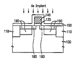
- a third ion implantation process for implanting n-type impurity ions into the semiconductor substrate 100 on which the fluorine ion implantation region 160 and the halo ion implantation region 170 are formed is performed. This implantation is represented by the arrows in FIG. 5 .
- arsenic (As) ions are implanted with an ion implantation energy of about 5 to 50 keV and a concentration of about 1 ⁇ 10 15 to 5 ⁇ 10 15 ions/cm 2 .
- a thermal process is performed to diffuse the p-type halo ions and the n-type impurity ions.
- One example thermal process that may be used is a rapid thermal process (RTP) performed at a temperature of 800 to 1000° C. for 10 to 30 seconds in an atmosphere of N 2 .
- RTP rapid thermal process
- source/drain extension regions 180 are formed and a halo region 190 is formed at a side and a bottom of the source/drain extension regions 180 .
- FIG. 6 is a graphical diagram showing concentration distributions of halo impurity ions depending on fluorine implantation energy in a method for forming a halo region in an NMOS transistor in accordance with the disclosed method. From FIG. 6 , it can be seen that a case in which the BF 2 ions are implanted after the fluorine (F) ions are implanted, as disclosed herein for forming the halo region in the NMOS transistor, has a profile steeper than that of a case where only the BF 2 ions are implanted without implanting the fluorine (F) ions, thereby showing improvement of the halo profile.
- halo ions are concentrated into a projected range (Rp) of fluorine (F) ions by implanting the halo ions after implanting fluorine ions, and then performing a diffusion process using the same thermal process. Accordingly, a junction profile of the halo ions can be easily controlled by adjusting the projected range of the fluorine ions.
- methods for forming halo regions in NMOS transistors include controlling a profile of boron ions.
- a method for forming a halo region in a NMOS transistor includes forming, on a channel region of a semiconductor substrate, a structure having a gate insulation film pattern and a gate conductive film pattern stacked sequentially.
- the method may also include forming an ion implantation buffer film on an exposed surface of the semiconductor substrate and the gate conductive film pattern, performing a first ion implantation process for injecting fluorine ions into the semiconductor substrate, performing a second ion implantation process for implanting p-type halo ions into the semiconductor substrate, performing a third ion implantation process for implanting n-type impurity ions into the semiconductor substrate, and diffusing the p-type halo ions and the n-type impurity ions using a thermal process.
- the ion implantation buffer film is formed using an oxide film. Additionally, in the first ion implantation process, the fluorine ions may be implanted with an ion implantation energy of about 5 to 50 keV, a concentration of about 5 ⁇ 10 14 to 5 ⁇ 10 15 ions/cm 2 , and an implantation gradient of about 20° to 30°.
- BF 2 ions are implanted with an ion implantation energy of about 10 to 40 keV, a concentration of about 1 ⁇ 10 14 to 1 ⁇ 10 15 ions/cm 2 , and an implantation gradient of about 20° to 30°.
- the thermal process may include a rapid thermal process performed at a temperature of 800 to 1000° C. for 10 to 30 seconds in an atmosphere of N 2 .
Landscapes
- Insulated Gate Type Field-Effect Transistor (AREA)
- Metal-Oxide And Bipolar Metal-Oxide Semiconductor Integrated Circuits (AREA)
Abstract
Description
Claims (18)
Applications Claiming Priority (2)
| Application Number | Priority Date | Filing Date | Title |
|---|---|---|---|
| KR10-2003-0098384A KR100521440B1 (en) | 2003-12-27 | 2003-12-27 | Method for fabricating the halo region in NMOS transistor |
| KR10-2003-0098384 | 2003-12-27 |
Publications (2)
| Publication Number | Publication Date |
|---|---|
| US20050142821A1 US20050142821A1 (en) | 2005-06-30 |
| US7157357B2 true US7157357B2 (en) | 2007-01-02 |
Family
ID=34698616
Family Applications (1)
| Application Number | Title | Priority Date | Filing Date |
|---|---|---|---|
| US10/998,868 Expired - Fee Related US7157357B2 (en) | 2003-12-27 | 2004-11-29 | Methods of forming halo regions in NMOS transistors |
Country Status (2)
| Country | Link |
|---|---|
| US (1) | US7157357B2 (en) |
| KR (1) | KR100521440B1 (en) |
Cited By (4)
| Publication number | Priority date | Publication date | Assignee | Title |
|---|---|---|---|---|
| US20090233410A1 (en) * | 2008-03-13 | 2009-09-17 | Chen-Hua Yu | Self-Aligned Halo/Pocket Implantation for Reducing Leakage and Source/Drain Resistance in MOS Devices |
| US20110163379A1 (en) * | 2010-01-07 | 2011-07-07 | International Business Machines Corporation | Body-Tied Asymmetric P-Type Field Effect Transistor |
| US20110163380A1 (en) * | 2010-01-07 | 2011-07-07 | International Business Machines Corporation | Body-Tied Asymmetric N-Type Field Effect Transistor |
| US8735951B2 (en) | 2010-12-23 | 2014-05-27 | Samsung Electronics Co., Ltd. | Semiconductor device having diffusion barrier element injection region |
Families Citing this family (3)
| Publication number | Priority date | Publication date | Assignee | Title |
|---|---|---|---|---|
| US7701011B2 (en) * | 2006-08-15 | 2010-04-20 | Kovio, Inc. | Printed dopant layers |
| US8283708B2 (en) * | 2009-09-18 | 2012-10-09 | Micron Technology, Inc. | Semiconductor devices and methods of forming semiconductor devices having diffusion regions of reduced width |
| CN102386075A (en) * | 2010-08-27 | 2012-03-21 | 中芯国际集成电路制造(上海)有限公司 | Lightly-doped groove injection method |
Citations (12)
| Publication number | Priority date | Publication date | Assignee | Title |
|---|---|---|---|---|
| US5466612A (en) * | 1992-03-11 | 1995-11-14 | Matsushita Electronics Corp. | Method of manufacturing a solid-state image pickup device |
| US5885886A (en) * | 1996-12-26 | 1999-03-23 | Lg Semicon Co., Ltd. | Method for manufacturing semiconductor device |
| US6194278B1 (en) | 1999-06-21 | 2001-02-27 | Infineon Technologies North America Corp. | Device performance by employing an improved method for forming halo implants |
| US6362054B1 (en) | 2000-03-13 | 2002-03-26 | Agere Systems Guardian Corp. | Method for fabricating MOS device with halo implanted region |
| US6518136B2 (en) | 2000-12-14 | 2003-02-11 | International Business Machines Corporation | Sacrificial polysilicon sidewall process and rapid thermal spike annealing for advance CMOS fabrication |
| US6579751B2 (en) | 1999-09-01 | 2003-06-17 | Micron Technology, Inc. | Semiconductor processing methods of forming integrated circuitry |
| US6589847B1 (en) | 2000-08-03 | 2003-07-08 | Advanced Micro Devices, Inc. | Tilted counter-doped implant to sharpen halo profile |
| US20040150020A1 (en) * | 2002-08-27 | 2004-08-05 | Elpida Memory, Inc. | Semiconductor device and method of producing the same |
| US20040232516A1 (en) * | 2001-07-18 | 2004-11-25 | Matsushita Electric Industrial Co., Ltd. | Semiconductor device and method for manufacturing the same |
| US6853037B2 (en) * | 2000-06-05 | 2005-02-08 | Nec Electronics Corporation | Fabrication of low power CMOS device with high reliability |
| US20050110098A1 (en) * | 2002-03-15 | 2005-05-26 | Takuya Yoshihara | Semiconductor device and its manufacturing method |
| US20050151172A1 (en) * | 2001-10-02 | 2005-07-14 | Hisashi Takemura | Semiconductor device and its manufacturing method |
Family Cites Families (9)
| Publication number | Priority date | Publication date | Assignee | Title |
|---|---|---|---|---|
| US4731055A (en) * | 1986-08-25 | 1988-03-15 | Becton, Dickinson And Company | Blood flow conduit |
| JPH07312353A (en) * | 1994-05-17 | 1995-11-28 | Fuji Electric Co Ltd | Method for manufacturing semiconductor device |
| US5993382A (en) * | 1996-11-27 | 1999-11-30 | Horizon Medical Products, Inc. | Lighted catheter device and method for use and manufacture thereof |
| US6022769A (en) * | 1997-12-23 | 2000-02-08 | Texas Instruments -- Acer Incorporated | Method of making self-aligned silicided MOS transistor with ESD protection improvement |
| US6472281B2 (en) * | 1998-02-03 | 2002-10-29 | Matsushita Electronics Corporation | Method for fabricating semiconductor device using a CVD insulator film |
| JP4108950B2 (en) * | 2001-09-12 | 2008-06-25 | 株式会社エヌ・ティ・ティ・ドコモ | HANDOVER CONTROL DEVICE, RADIO TERMINAL, EDGE ROUTER, ROUTER, MOBILE COMMUNICATION SYSTEM AND HANDOVER CONTROL METHOD |
| US6767778B2 (en) * | 2002-08-29 | 2004-07-27 | Micron Technology, Inc. | Low dose super deep source/drain implant |
| US6670682B1 (en) * | 2002-08-29 | 2003-12-30 | Micron Technology, Inc. | Multilayered doped conductor |
| US7016328B2 (en) * | 2003-06-24 | 2006-03-21 | Tropos Networks, Inc. | Method for allowing a client to access a wireless system |
-
2003
- 2003-12-27 KR KR10-2003-0098384A patent/KR100521440B1/en not_active Expired - Fee Related
-
2004
- 2004-11-29 US US10/998,868 patent/US7157357B2/en not_active Expired - Fee Related
Patent Citations (12)
| Publication number | Priority date | Publication date | Assignee | Title |
|---|---|---|---|---|
| US5466612A (en) * | 1992-03-11 | 1995-11-14 | Matsushita Electronics Corp. | Method of manufacturing a solid-state image pickup device |
| US5885886A (en) * | 1996-12-26 | 1999-03-23 | Lg Semicon Co., Ltd. | Method for manufacturing semiconductor device |
| US6194278B1 (en) | 1999-06-21 | 2001-02-27 | Infineon Technologies North America Corp. | Device performance by employing an improved method for forming halo implants |
| US6579751B2 (en) | 1999-09-01 | 2003-06-17 | Micron Technology, Inc. | Semiconductor processing methods of forming integrated circuitry |
| US6362054B1 (en) | 2000-03-13 | 2002-03-26 | Agere Systems Guardian Corp. | Method for fabricating MOS device with halo implanted region |
| US6853037B2 (en) * | 2000-06-05 | 2005-02-08 | Nec Electronics Corporation | Fabrication of low power CMOS device with high reliability |
| US6589847B1 (en) | 2000-08-03 | 2003-07-08 | Advanced Micro Devices, Inc. | Tilted counter-doped implant to sharpen halo profile |
| US6518136B2 (en) | 2000-12-14 | 2003-02-11 | International Business Machines Corporation | Sacrificial polysilicon sidewall process and rapid thermal spike annealing for advance CMOS fabrication |
| US20040232516A1 (en) * | 2001-07-18 | 2004-11-25 | Matsushita Electric Industrial Co., Ltd. | Semiconductor device and method for manufacturing the same |
| US20050151172A1 (en) * | 2001-10-02 | 2005-07-14 | Hisashi Takemura | Semiconductor device and its manufacturing method |
| US20050110098A1 (en) * | 2002-03-15 | 2005-05-26 | Takuya Yoshihara | Semiconductor device and its manufacturing method |
| US20040150020A1 (en) * | 2002-08-27 | 2004-08-05 | Elpida Memory, Inc. | Semiconductor device and method of producing the same |
Cited By (7)
| Publication number | Priority date | Publication date | Assignee | Title |
|---|---|---|---|---|
| US20090233410A1 (en) * | 2008-03-13 | 2009-09-17 | Chen-Hua Yu | Self-Aligned Halo/Pocket Implantation for Reducing Leakage and Source/Drain Resistance in MOS Devices |
| US8822293B2 (en) * | 2008-03-13 | 2014-09-02 | Taiwan Semiconductor Manufacturing Company, Ltd. | Self-aligned halo/pocket implantation for reducing leakage and source/drain resistance in MOS devices |
| US20110163379A1 (en) * | 2010-01-07 | 2011-07-07 | International Business Machines Corporation | Body-Tied Asymmetric P-Type Field Effect Transistor |
| US20110163380A1 (en) * | 2010-01-07 | 2011-07-07 | International Business Machines Corporation | Body-Tied Asymmetric N-Type Field Effect Transistor |
| US8426917B2 (en) | 2010-01-07 | 2013-04-23 | International Business Machines Corporation | Body-tied asymmetric P-type field effect transistor |
| US8643107B2 (en) | 2010-01-07 | 2014-02-04 | International Business Machines Corporation | Body-tied asymmetric N-type field effect transistor |
| US8735951B2 (en) | 2010-12-23 | 2014-05-27 | Samsung Electronics Co., Ltd. | Semiconductor device having diffusion barrier element injection region |
Also Published As
| Publication number | Publication date |
|---|---|
| KR20050066900A (en) | 2005-06-30 |
| KR100521440B1 (en) | 2005-10-13 |
| US20050142821A1 (en) | 2005-06-30 |
Similar Documents
| Publication | Publication Date | Title |
|---|---|---|
| US6475887B1 (en) | Method of manufacturing semiconductor device | |
| CN1307696C (en) | Fabrication method of semiconductor device with ultra-shallow and ultra-steep reverse surface channel | |
| US5970353A (en) | Reduced channel length lightly doped drain transistor using a sub-amorphous large tilt angle implant to provide enhanced lateral diffusion | |
| KR100588786B1 (en) | Semiconductor device manufacturing method | |
| US5963799A (en) | Blanket well counter doping process for high speed/low power MOSFETs | |
| US5821147A (en) | Integrated circuit fabrication | |
| US6051459A (en) | Method of making N-channel and P-channel IGFETs using selective doping and activation for the N-channel gate | |
| US6294432B1 (en) | Super halo implant combined with offset spacer process | |
| US7157357B2 (en) | Methods of forming halo regions in NMOS transistors | |
| KR100574172B1 (en) | Manufacturing method of semiconductor device | |
| US9881841B2 (en) | Methods for fabricating integrated circuits with improved implantation processes | |
| US8962441B2 (en) | Transistor device with improved source/drain junction architecture and methods of making such a device | |
| US20070194376A1 (en) | MOS transistors and methods of manufacturing the same | |
| KR100519507B1 (en) | Method for Forming Semi-conductor Device | |
| US6096588A (en) | Method of making transistor with selectively doped channel region for threshold voltage control | |
| US6720227B1 (en) | Method of forming source/drain regions in a semiconductor device | |
| CN111129141A (en) | Preparation method of semiconductor device and semiconductor device obtained by preparation method | |
| KR100588787B1 (en) | Semiconductor device manufacturing method | |
| KR100598284B1 (en) | Semiconductor device manufacturing method | |
| KR100552853B1 (en) | Impurity Injection Method for Threshold Voltage Control of n-channel Morse Transistor | |
| KR20010051564A (en) | A method to create Halo implanted region under the channel with RTA in CMOS technology | |
| KR100600253B1 (en) | Semiconductor device manufacturing method | |
| KR101128699B1 (en) | Method for manufacturing a semiconductor device | |
| KR20050104209A (en) | Method for manufacturing pmos transistor | |
| KR20000062536A (en) | Semiconductor device and method for manufacturing same |
Legal Events
| Date | Code | Title | Description |
|---|---|---|---|
| AS | Assignment |
Owner name: DONGBU ELECTRONICS CO., LTD., KOREA, REPUBLIC OF Free format text: ASSIGNMENT OF ASSIGNORS INTEREST;ASSIGNOR:KIM, HAK-DONG;REEL/FRAME:016052/0662 Effective date: 20041126 |
|
| AS | Assignment |
Owner name: DONGBU ELECTRONICS CO., LTD.,KOREA, REPUBLIC OF Free format text: CHANGE OF NAME;ASSIGNOR:DONGANAM SEMICONDUCTOR INC.;REEL/FRAME:017749/0335 Effective date: 20060328 Owner name: DONGBU ELECTRONICS CO., LTD., KOREA, REPUBLIC OF Free format text: CHANGE OF NAME;ASSIGNOR:DONGANAM SEMICONDUCTOR INC.;REEL/FRAME:017749/0335 Effective date: 20060328 |
|
| AS | Assignment |
Owner name: DONGBU ELECTRONICS CO., LTD., KOREA, REPUBLIC OF Free format text: CORRECTIVE ASSIGNMENT TO CORRECT THE ASSIGNOR PREVIOUSLY RECORDED ON REEL 017749 FRAME 0335;ASSIGNOR:DONGBUANAM SEMICONDUCTOR INC.;REEL/FRAME:017821/0670 Effective date: 20060328 Owner name: DONGBU ELECTRONICS CO., LTD.,KOREA, REPUBLIC OF Free format text: CORRECTIVE ASSIGNMENT TO CORRECT THE ASSIGNOR PREVIOUSLY RECORDED ON REEL 017749 FRAME 0335. ASSIGNOR(S) HEREBY CONFIRMS THE ASSIGNOR SHOULD BE "DONGBUANAM SEMICONDUCTOR INC.";ASSIGNOR:DONGBUANAM SEMICONDUCTOR INC.;REEL/FRAME:017821/0670 Effective date: 20060328 Owner name: DONGBU ELECTRONICS CO., LTD., KOREA, REPUBLIC OF Free format text: CORRECTIVE ASSIGNMENT TO CORRECT THE ASSIGNOR PREVIOUSLY RECORDED ON REEL 017749 FRAME 0335. ASSIGNOR(S) HEREBY CONFIRMS THE ASSIGNOR SHOULD BE "DONGBUANAM SEMICONDUCTOR INC.";ASSIGNOR:DONGBUANAM SEMICONDUCTOR INC.;REEL/FRAME:017821/0670 Effective date: 20060328 |
|
| FEPP | Fee payment procedure |
Free format text: PAYOR NUMBER ASSIGNED (ORIGINAL EVENT CODE: ASPN); ENTITY STATUS OF PATENT OWNER: LARGE ENTITY |
|
| FPAY | Fee payment |
Year of fee payment: 4 |
|
| FPAY | Fee payment |
Year of fee payment: 8 |
|
| AS | Assignment |
Owner name: DONGBU HITEK CO., LTD., KOREA, REPUBLIC OF Free format text: MERGER AND CHANGE OF NAME;ASSIGNORS:DONGBU ELECTRONICS CO., LTD.;DONGBU HITEK CO., LTD.;REEL/FRAME:044533/0523 Effective date: 20070503 |
|
| AS | Assignment |
Owner name: DB HITEK CO., LTD, KOREA, REPUBLIC OF Free format text: CHANGE OF NAME;ASSIGNOR:DONGBU HITEK CO., LTD.;REEL/FRAME:044555/0913 Effective date: 20171101 |
|
| FEPP | Fee payment procedure |
Free format text: MAINTENANCE FEE REMINDER MAILED (ORIGINAL EVENT CODE: REM.); ENTITY STATUS OF PATENT OWNER: LARGE ENTITY |
|
| LAPS | Lapse for failure to pay maintenance fees |
Free format text: PATENT EXPIRED FOR FAILURE TO PAY MAINTENANCE FEES (ORIGINAL EVENT CODE: EXP.); ENTITY STATUS OF PATENT OWNER: LARGE ENTITY |
|
| STCH | Information on status: patent discontinuation |
Free format text: PATENT EXPIRED DUE TO NONPAYMENT OF MAINTENANCE FEES UNDER 37 CFR 1.362 |
|
| FP | Lapsed due to failure to pay maintenance fee |
Effective date: 20190102 |
|
| AS | Assignment |
Owner name: COLUMBA TECHNOLOGIES INC., CANADA Free format text: ASSIGNMENT OF ASSIGNORS INTEREST;ASSIGNOR:DB HITEK CO., LTD.;REEL/FRAME:049709/0857 Effective date: 20190125 |