US7134882B2 - Connector having a built-in electronic part - Google Patents
Connector having a built-in electronic part Download PDFInfo
- Publication number
- US7134882B2 US7134882B2 US10/541,038 US54103805A US7134882B2 US 7134882 B2 US7134882 B2 US 7134882B2 US 54103805 A US54103805 A US 54103805A US 7134882 B2 US7134882 B2 US 7134882B2
- Authority
- US
- United States
- Prior art keywords
- base member
- connector
- electronic component
- conductive pattern
- contact
- Prior art date
- Legal status (The legal status is an assumption and is not a legal conclusion. Google has not performed a legal analysis and makes no representation as to the accuracy of the status listed.)
- Expired - Fee Related
Links
Images


Classifications
-
- H—ELECTRICITY
- H05—ELECTRIC TECHNIQUES NOT OTHERWISE PROVIDED FOR
- H05K—PRINTED CIRCUITS; CASINGS OR CONSTRUCTIONAL DETAILS OF ELECTRIC APPARATUS; MANUFACTURE OF ASSEMBLAGES OF ELECTRICAL COMPONENTS
- H05K1/00—Printed circuits
- H05K1/02—Details
- H05K1/11—Printed elements for providing electric connections to or between printed circuits
- H05K1/119—Details of rigid insulating substrates therefor, e.g. three-dimensional details
-
- H—ELECTRICITY
- H01—ELECTRIC ELEMENTS
- H01R—ELECTRICALLY-CONDUCTIVE CONNECTIONS; STRUCTURAL ASSOCIATIONS OF A PLURALITY OF MUTUALLY-INSULATED ELECTRICAL CONNECTING ELEMENTS; COUPLING DEVICES; CURRENT COLLECTORS
- H01R13/00—Details of coupling devices of the kinds covered by groups H01R12/70 or H01R24/00 - H01R33/00
- H01R13/66—Structural association with built-in electrical component
-
- H—ELECTRICITY
- H01—ELECTRIC ELEMENTS
- H01R—ELECTRICALLY-CONDUCTIVE CONNECTIONS; STRUCTURAL ASSOCIATIONS OF A PLURALITY OF MUTUALLY-INSULATED ELECTRICAL CONNECTING ELEMENTS; COUPLING DEVICES; CURRENT COLLECTORS
- H01R29/00—Coupling parts for selective co-operation with a counterpart in different ways to establish different circuits, e.g. for voltage selection, for series-parallel selection, programmable connectors
-
- H—ELECTRICITY
- H05—ELECTRIC TECHNIQUES NOT OTHERWISE PROVIDED FOR
- H05K—PRINTED CIRCUITS; CASINGS OR CONSTRUCTIONAL DETAILS OF ELECTRIC APPARATUS; MANUFACTURE OF ASSEMBLAGES OF ELECTRICAL COMPONENTS
- H05K1/00—Printed circuits
- H05K1/02—Details
- H05K1/14—Structural association of two or more printed circuits
-
- H—ELECTRICITY
- H05—ELECTRIC TECHNIQUES NOT OTHERWISE PROVIDED FOR
- H05K—PRINTED CIRCUITS; CASINGS OR CONSTRUCTIONAL DETAILS OF ELECTRIC APPARATUS; MANUFACTURE OF ASSEMBLAGES OF ELECTRICAL COMPONENTS
- H05K1/00—Printed circuits
- H05K1/02—Details
- H05K1/0284—Details of three-dimensional rigid printed circuit boards
-
- H—ELECTRICITY
- H05—ELECTRIC TECHNIQUES NOT OTHERWISE PROVIDED FOR
- H05K—PRINTED CIRCUITS; CASINGS OR CONSTRUCTIONAL DETAILS OF ELECTRIC APPARATUS; MANUFACTURE OF ASSEMBLAGES OF ELECTRICAL COMPONENTS
- H05K1/00—Printed circuits
- H05K1/02—Details
- H05K1/14—Structural association of two or more printed circuits
- H05K1/141—One or more single auxiliary printed circuits mounted on a main printed circuit, e.g. modules, adapters
-
- H—ELECTRICITY
- H05—ELECTRIC TECHNIQUES NOT OTHERWISE PROVIDED FOR
- H05K—PRINTED CIRCUITS; CASINGS OR CONSTRUCTIONAL DETAILS OF ELECTRIC APPARATUS; MANUFACTURE OF ASSEMBLAGES OF ELECTRICAL COMPONENTS
- H05K1/00—Printed circuits
- H05K1/18—Printed circuits structurally associated with non-printed electric components
- H05K1/182—Printed circuits structurally associated with non-printed electric components associated with components mounted in the printed circuit board, e.g. insert mounted components [IMC]
- H05K1/183—Components mounted in and supported by recessed areas of the printed circuit board
-
- H—ELECTRICITY
- H05—ELECTRIC TECHNIQUES NOT OTHERWISE PROVIDED FOR
- H05K—PRINTED CIRCUITS; CASINGS OR CONSTRUCTIONAL DETAILS OF ELECTRIC APPARATUS; MANUFACTURE OF ASSEMBLAGES OF ELECTRICAL COMPONENTS
- H05K2201/00—Indexing scheme relating to printed circuits covered by H05K1/00
- H05K2201/09—Shape and layout
- H05K2201/09009—Substrate related
- H05K2201/09045—Locally raised area or protrusion of insulating substrate
-
- H—ELECTRICITY
- H05—ELECTRIC TECHNIQUES NOT OTHERWISE PROVIDED FOR
- H05K—PRINTED CIRCUITS; CASINGS OR CONSTRUCTIONAL DETAILS OF ELECTRIC APPARATUS; MANUFACTURE OF ASSEMBLAGES OF ELECTRICAL COMPONENTS
- H05K2201/00—Indexing scheme relating to printed circuits covered by H05K1/00
- H05K2201/09—Shape and layout
- H05K2201/09009—Substrate related
- H05K2201/09118—Moulded substrate
-
- H—ELECTRICITY
- H05—ELECTRIC TECHNIQUES NOT OTHERWISE PROVIDED FOR
- H05K—PRINTED CIRCUITS; CASINGS OR CONSTRUCTIONAL DETAILS OF ELECTRIC APPARATUS; MANUFACTURE OF ASSEMBLAGES OF ELECTRICAL COMPONENTS
- H05K2201/00—Indexing scheme relating to printed circuits covered by H05K1/00
- H05K2201/10—Details of components or other objects attached to or integrated in a printed circuit board
- H05K2201/10007—Types of components
- H05K2201/10189—Non-printed connector
-
- H—ELECTRICITY
- H05—ELECTRIC TECHNIQUES NOT OTHERWISE PROVIDED FOR
- H05K—PRINTED CIRCUITS; CASINGS OR CONSTRUCTIONAL DETAILS OF ELECTRIC APPARATUS; MANUFACTURE OF ASSEMBLAGES OF ELECTRICAL COMPONENTS
- H05K3/00—Apparatus or processes for manufacturing printed circuits
- H05K3/40—Forming printed elements for providing electric connections to or between printed circuits
- H05K3/403—Edge contacts; Windows or holes in the substrate having plural connections on the walls thereof
Definitions
- the present invention relates to a connector with an electronic component built-in.
- FIG. 9A shows a configuration of a conventional connector with an electric component built-in, which is, for example shown in Japanese Laid-Open Patent Publication No. 2002-198132.
- a capacitor 101 is used as an electronic component, and two lead terminals 104 a and 104 b of the capacitor 101 are respectively soldered to a conductor 102 of a cable and an inner conductor terminal 103 of a connector, so that the conductor 102 and the inner conductor terminal 103 are electrically connected via the capacitor 101 .
- the capacitor 101 , conductor 102 and the inner conductor terminal 103 are insulated by an insulating material 105 and an outside conductor terminal 106 .
- FIG. 9B shows a configuration of another conventional connector with an electronic component built-in, for example, shown in Japanese Laid-Open Patent Publication No. 2002-184532.
- electrodes 112 a and 112 b provided on both ends of a chip type electronic component 111 are respectively soldered to a rear end portion 113 a of a fitting terminal 113 and a rear end portion 114 a of a connecting terminal 114 , so that the integrated chip type electronic component 111 , the fitting terminal 113 and the connecting terminal 114 are fixed on a connector housing 115 .
- the present invention is made to solve the problems of the above-mentioned prior arts, and the object of the invention is to provide a connector which can make a modification of a conductive pattern of a connector easily, and can realize the increase of degrees of freedom of design of electric wiring and enhancement of mounting workability of an electronic component.
- a connector with an electronic component built-in in accordance with an aspect of the present invention comprises: a base member formed of a three-dimensional formation circuit board; terminals formed on said base member and electrically connected to wiring pattern of a mother board; a fitting portion formed on said base member, and to be fitted to a counterpart connector; contacts arranged on said fitting portion and to be electrically connected with contacting terminal portions of said counterpart connector; an electric component disposed on said base member; and a conductive pattern formed on said base member for electrically connecting said terminals or said contacts with said electronic component.
- the conductive pattern, the terminals and the contacts are formed on the base member of the three-dimensional formation circuit board, it is relatively easy to modify the conductive pattern depending on application. Furthermore, since the superficial area of the base member of the three-dimensional formation circuit board is relatively larger, it is possible to form a complicated electric wiring, so that it is possible to built-in a lot of electronic components in the connector. As a result, degrees of freedom of design of electric wiring can be increased. Still furthermore, since the electronic component is disposed on the base member of the three-dimensional formation circuit board, it is possible to connect the electronic component by reflow soldering, so that the mounting workability of the electronic component is increased.
- FIG. 1 is a sectional view showing a configuration of a connector with an electronic component built-in in accordance with a first embodiment of the present invention.
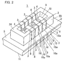
- FIG. 2 is a perspective view showing a configuration of a header of the connector in accordance with the first embodiment.
- FIG. 3 is a flowchart showing manufacturing processes of a base member of the connector (or the header) by electrolytic plating in accordance with the first embodiment.
- FIG. 4 is a sectional view showing a configuration of a base member just before implementation by above manufacturing process.
- FIG. 5 is a sectional view showing a configuration of a modification of the connector in accordance with the first embodiment.
- FIG. 6 is a sectional view showing a configuration of a connector with an electronic component built-in in accordance with a second embodiment of the present invention.
- FIG. 7 is a sectional view showing a configuration of a modification of the connector in accordance with the second embodiment.
- FIG. 8 is a sectional view showing a configuration of a connector with an electronic component built-in in accordance with a third embodiment of the present invention.
- FIG. 9A is a sectional view showing a configuration of a conventional connector with an electronic component built-in
- FIG. 9B is a perspective view showing a configuration of another conventional connector with an electronic component built-in.
- FIG. 1 is a sectional view showing a configuration of the connector in accordance with the first embodiment.
- the connector in accordance with the first embodiment is comprised of a header 1 and a socket 6 , and an electronic component 4 is built-in to the header 1 .
- FIG. 2 is a perspective view showing a configuration of the header 1 .
- the header 1 comprises a base member 2 of a three-dimensional formation circuit board which is formed of, for example, thermosetting resin, ceramics, or the like, a conductive pattern 3 formed on the base member 2 , an electronic component 4 mounted on the base member 2 , and so on.
- the base member 2 has a rectangular plane portion 5 and a fitting portion 29 formed on a center of the plane portion 5 .
- the fitting portion 29 has a substantially rectangular parallelepiped shape, and it is to be fitted to a concavity 61 formed to the socket 6 which is a counterpart.
- a concavity 9 of rectangular parallelepiped shape having a depth measure that is long than a height measure of the fitting portion 29 from the plane portion 5 is formed.
- the electronic component 4 is mounted by soldering, so that it is electrically connected to a conductive pattern 3 a .
- a plurality of through holes 12 is formed for penetrating from the bottom face 10 of the concavity 9 to a back face portion 11 of the base member 2 .
- a pair of groove portions 13 is formed on the back face portion 11 along longitudinal direction of the base member 2 .
- Terminals 16 which are to be soldered to a wiring pattern 15 of a mother board 14 when the base member 2 is fixed on the mother board 14 , are formed with a conductive pattern 3 on both end portions in width direction of the back face portion 11 of the base member 2 . Furthermore, contacts 8 , which are to be electrically connected to contact terminal portions 7 of the socket 6 as the counterpart connector, are integrally formed with the conductive pattern 3 along outer side faces of the fitting portion 29 .
- Each terminal 16 has a parallel face 16 c parallel to the wiring pattern 15 of the mother board 14 at a center portion thereof, and an outer inclined face (including perpendicularity) 16 a and an inner inclined face 16 b at both end portion thereof which are not parallel to the wiring pattern 15 of the mother board 14 . Fillets of solder are formed on the inclined faces 16 a and 16 b , so that the terminal 16 is electrically connected to the wiring pattern 15 of the mother board 14 .
- a conductive pattern 3 b is formed along an inner peripheral surface of each through hole 12 , so that the conductive pattern 3 a on the bottom face 10 of the concavity 9 and the conductive pattern 3 c on the back face portion 11 are electrically connected, and the contacts 8 and the terminals 16 are electrically connected through electronic component 4 .
- FIG. 3 is a flowchart showing the manufacturing process of the base member 2
- FIG. 4 is a sectional view showing a configuration of the base member 2 just before implementation.
- a base substance of three-dimensional formation circuit board is molded (S 1 ). Subsequently, a Cu film is formed by sputtering technique to cover the entire surface of the base substance (S 2 ), and a Cu film is patterned by using a laser beam (S 3 ). Furthermore, electrolytic plating of Cu is performed on only a part which it is necessary (S 4 ), and Cu of unnecessary portion is removed by etching (S 5 ). After that, electrolytic plating of Ni is performed to the base substance (S 6 ), and electrolytic plating of Au is performed thereto (S 7 ). Finally, as shown in FIG. 4 , the base member 2 and the feeding side 18 of plating current are cut off in disconnecting portion 17 on the plane portion 5 (S 8 ). The base member 2 comprised of the three-dimensional formation circuit board on which conductive pattern 3 is formed is finished.
- the contacts 8 and the terminals 16 are integrally formed with the conductive pattern 3 on the base member 2 . Therefore, the contacts 8 , the terminals 16 and the conductive pattern 3 can easily be modified depending on purpose. Furthermore, since a superficial area of the base member 2 of the three-dimensional formation circuit board is relatively larger, complicated electric wiring can be formed, and a lot of electronic components 4 can be mounted on the base member 2 . As a result, degrees of freedom of design can be increased.
- the electronic component 4 is disposed on the bottom face 10 of the concavity 9 of base member 2 , namely, on a plane portion, reflow soldering can be used for soldering of the electronic component 4 , mounting workability of the electronic component 4 is improved, and yield of manufacture can be increased.
- FIG. 5 a configuration of a modification of the connector in accordance with the first embodiment is shown in FIG. 5 .
- a sealant 19 is filled in the cavity 9 so as to cover and seal the electronic component 4 .
- the other structure it is similar to the above-mentioned case, so that the description of it is omitted. In this way, even though a number of steps of the manufacturing processes is increased and it causes the increase of the cost a little by covering and sealing the electronic component 4 , it is possible to protect the electronic component 4 further to the above-mentioned effects. The same goes for in the following embodiments.
- FIG. 6 is a sectional view showing a configuration of a header of a connector in accordance with the second embodiment.
- holding apertures 20 each for holding a contact terminal 21 of metal are formed penetrating through the pale portion 5 and the groove portions 13 of the base member 2 and along outer side faces of the fitting portion 29 , in the second embodiment.
- Conductive patterns 3 d are formed on inner peripheral surfaces of the holding apertures 20 .
- the contact terminal 21 has a substantially L-shaped section, and a longitudinal side portion 21 a serves as a contact 8 , and a transversal side portion 21 b serves as a terminal 16 .
- the contact terminal 21 is press fitted into the holding aperture 20 in a manner so that the longitudinal side portion 21 a is directed upward from the back face side of the base member 2 under a condition that a front end of the transversal side portion 21 b is directed outward.
- the direction of press fitting of the contact terminal 21 to the holding aperture 20 of the base member 2 is set to be perpendicular to the direction of press contact of the contact terminal portion 7 of the socket 6 as the counter part connector (see FIG. 7 ).
- a portion among the longitudinal side portion 21 a press fitted into the holding aperture 20 serves as a portion to be held.
- the longitudinal side portion 21 a of the contact terminal 21 serving as a contact 8 goes along an outer side face of the fitting portion 29 , and a lower end of the longitudinal side portion 21 b is electrically connected to the conductive pattern 3 d formed on an inner peripheral surface of the holding aperture 20 .
- the contact terminal 21 is fixed on the base member 2 , and the transversal side portion 21 b is electrically connected to the conductive pattern 3 e formed in neighborhood of an edge in width direction on the back face portion 11 of the base member 2 .
- the electric connection of the contact terminal 21 with the conductive pattern 3 and the mechanical connection of the contact terminal 21 and the base member 2 are performed by merely press fitting the longitudinal side portion 21 a of the contact terminal 21 into the holding aperture 20 .
- the contact terminal 21 and the conductive pattern 3 are not fixed by soldering, it is possible to prevent the flaking of the conductive pattern 3 from the base member 2 due to pressure received from the contact terminal portion 7 of the socket 6 .
- the contact terminal 21 having a substantially L-shaped section is used as a contact 8 for electrically connecting the contact terminal portion 7 of the socket as the counterpart connector with the base member 2 , durability of the contact body 8 is increased.
- FIG. 7 a configuration of a modification of the connector in accordance with the second embodiment is shown in FIG. 7 .
- the contact terminal 21 and the conductive pattern 3 are soldered in the groove portion 13 (soldered portion is designated by a numeric symbol 22 ) for electrically connecting and mechanically fixing the contact terminal 21 with the conductive pattern 3 .
- the contact terminal 21 and the conductive pattern 3 are fixed by soldering.
- the direction of press fitting of the contact terminal 21 into the holding aperture 20 of the base member 2 is set to be perpendicular to the direction of pressure received from the contact terminal portion 7 of the socket 6 , so that it is possible to reduce the load due to the contact pressure to the soldered portion 22 of the contact terminal 21 and the conductive pattern 3 , and it is possible to prevent the flaking of the conductive pattern 3 from the base member 2 due to the load.
- FIG. 8 is a sectional view showing a configuration of a header in of a connector in accordance with the third embodiment.
- press fitting apertures 23 each for holding a longer longitudinal side portion 27 a of a contact terminal 27 made of a metal are formed on the plane portion 5 of the base member 2 along outer side faces of the fitting portion 29 , in the third embodiment.
- holding apertures 25 each for folding a shorter longitudinal side portion 27 b of the contact terminal 27 are formed on upper faces 24 of the fitting portions 29 in directions perpendicular to a direction of contacting with the socket 6 as the counterpart connector.
- An open end 26 of the holding aperture 25 is formed so that a width of the open end 26 becomes gradually wider toward outside.
- a conductive pattern 3 f is formed on an inner peripheral surface of the holding aperture 25 .
- the contact terminal 27 is a metal band formed substantially U-shape having the longer longitudinal side portion 27 a , the shorter longitudinal side portion 27 b and a transversal side portion 27 c , and the longer longitudinal side portion 27 a serves as a contact 8 .
- the contact terminal 27 is held on the base member 2 in a manner so that the longer longitudinal side portion 27 a is press fitted into the press fitting aperture 23 and the shorter longitudinal side portion 27 b is press fitted into the holding aperture 25 from above the base member 2 .
- a neighboring portion of a free end of the longer longitudinal side portion 27 a and a neighboring portion of a free end of the shorter longitudinal side portion 27 b respectively serve as portions to be held which are press fitted into the press fitting aperture 23 and the holding aperture 25 .
- the shorter longitudinal side portion 27 b is connected to the conductive pattern 3 f formed on the inner peripheral surface of the holding aperture 25 , and the transversal side portion 27 c is contacted with a conductive pattern 3 g formed on the upper face 24 of the fitting portion 29 of the base member 2 .
- the contact terminal 27 and the conductive pattern 3 are soldered (soldered portion is designated by a numeric symbol 28 ) for electrically connecting and mechanically fixing the contact terminal 27 with the conductive pattern 3 .
- the longer longitudinal side portion 27 a of the contact terminal 27 along an outer side face of the fitting portion 29 of the base member 2 serves as a contact 8 .
- the contact terminal 27 is simply press fitted into the holding aperture 25 .
- a conductive paste can be used in substitution for soldering.
- the contact terminal 27 is used as a contact 8 which is electrically connected to the contact terminal portion 7 of the socket 6 which is a counterpart connector, durability of the contact 8 is increased. Furthermore, since the direction for press fitting the contact terminal 27 into the base member 2 is to be perpendicular to the direction of the contact pressure received from the socket 6 , it is possible to reduce the load to the soldered portion 28 of the contact terminal 27 and the conductive pattern 3 due to the contact pressure, and it is possible to prevent the flaking of the conductive pattern 3 from the base member 2 due to the load.
- the present invention is not limited to the connector used for the mother board as mentioned in each above embodiment.
- it can be used for a connector connected to an interface cable provided on a mobile phone or a PDA (Personal Digital Assistant).
- the connector with an electronic component built-in is not limited to the header constituting the connector as mentioned in each above embodiment.
- the electronic component may be built-in an interior of the socket which is a counterpart connector of the header.
Abstract
Description
Claims (8)
Applications Claiming Priority (3)
| Application Number | Priority Date | Filing Date | Title |
|---|---|---|---|
| JP2003301913A JP3956920B2 (en) | 2003-08-26 | 2003-08-26 | connector |
| JP2003-301913 | 2003-08-26 | ||
| PCT/JP2004/012106 WO2005020385A1 (en) | 2003-08-26 | 2004-08-24 | Connector having a built-in electronic part |
Publications (2)
| Publication Number | Publication Date |
|---|---|
| US20060183358A1 US20060183358A1 (en) | 2006-08-17 |
| US7134882B2 true US7134882B2 (en) | 2006-11-14 |
Family
ID=34213918
Family Applications (1)
| Application Number | Title | Priority Date | Filing Date |
|---|---|---|---|
| US10/541,038 Expired - Fee Related US7134882B2 (en) | 2003-08-26 | 2004-08-24 | Connector having a built-in electronic part |
Country Status (6)
| Country | Link |
|---|---|
| US (1) | US7134882B2 (en) |
| JP (1) | JP3956920B2 (en) |
| KR (1) | KR100775161B1 (en) |
| CN (1) | CN100409497C (en) |
| TW (1) | TWI247458B (en) |
| WO (1) | WO2005020385A1 (en) |
Cited By (6)
| Publication number | Priority date | Publication date | Assignee | Title |
|---|---|---|---|---|
| US20080070447A1 (en) * | 2006-09-04 | 2008-03-20 | Molex Incorporated | Socket connector |
| US7445466B1 (en) * | 2007-07-30 | 2008-11-04 | Cheng Uei Precision Industry Co., Ltd. | Board-to-board connector assembly |
| US20110083889A1 (en) * | 2007-06-25 | 2011-04-14 | Molex Incorporated | FPC-Based Relay Connector |
| US20110275228A1 (en) * | 2008-09-30 | 2011-11-10 | Molex Incorporated | Capacitively coupled connector for electronic device |
| US20140336930A1 (en) * | 2011-12-07 | 2014-11-13 | Atlantic Inertial Systems Limited | Electronic device |
| US9004925B2 (en) | 2009-01-30 | 2015-04-14 | Molex Incorporated | Capacitively coupled connector using liquid dielectric for improved performance |
Families Citing this family (12)
| Publication number | Priority date | Publication date | Assignee | Title |
|---|---|---|---|---|
| JP4563915B2 (en) * | 2005-10-21 | 2010-10-20 | ヒロセ電機株式会社 | Circuit board electrical connector |
| JP2009187809A (en) | 2008-02-07 | 2009-08-20 | Kyocera Elco Corp | Cable connector |
| US7955093B2 (en) * | 2009-02-05 | 2011-06-07 | Tyco Electronics Corporation | Connector assembly having electronic components mounted thereto |
| US8241067B2 (en) * | 2009-11-04 | 2012-08-14 | Amphenol Corporation | Surface mount footprint in-line capacitance |
| JP5296823B2 (en) * | 2011-03-17 | 2013-09-25 | イリソ電子工業株式会社 | Resin molded product and manufacturing method thereof |
| DE102013100197A1 (en) * | 2013-01-10 | 2014-07-10 | Continental Automotive Gmbh | Sensing unit for motor car, has injection molded plastic carrier which is positioned on opposite side to sensor element, and formed of electrical contacts with respect to the circuit board |
| US8888506B2 (en) * | 2013-01-29 | 2014-11-18 | Japan Aviation Electronics Industry, Limited | Connector |
| JP6436296B2 (en) | 2014-10-24 | 2018-12-12 | パナソニックIpマネジメント株式会社 | 3D circuit board and sensor module using the 3D circuit board |
| JP6638262B2 (en) | 2015-02-03 | 2020-01-29 | 株式会社オートネットワーク技術研究所 | Circuit components |
| CN105392320B (en) * | 2015-12-15 | 2018-05-29 | 深圳南方德尔汽车电子有限公司 | A kind of controller |
| CN206524474U (en) * | 2017-03-21 | 2017-09-26 | 京东方科技集团股份有限公司 | Bus bar connector, flexible PCB, contact panel and display device |
| DE102020102983A1 (en) | 2020-02-05 | 2021-08-05 | Harting Ag | Component carrier for arranging electrical components on a circuit board |
Citations (20)
| Publication number | Priority date | Publication date | Assignee | Title |
|---|---|---|---|---|
| US4490001A (en) * | 1983-02-07 | 1984-12-25 | Matsushita Electric Industrial Co., Ltd. | Dip carrier and socket |
| JPS6059379A (en) | 1983-09-13 | 1985-04-05 | Fuji Xerox Co Ltd | Inclination holding device of photosensitive body unit |
| JPH0349178A (en) * | 1989-07-18 | 1991-03-01 | Hitachi Ltd | Mounting structure for semiconductor device, mounting substrate and semiconductor device |
| US5355282A (en) * | 1991-08-30 | 1994-10-11 | Fujitsu Limited | Connector structure for modules in electronic apparatus |
| US5433617A (en) * | 1993-06-04 | 1995-07-18 | Framatome Connectors International | Connector assembly for printed circuit boards |
| JPH08236219A (en) | 1994-12-14 | 1996-09-13 | Whitaker Corp:The | Filter type electric connector and its preparation |
| US5588847A (en) * | 1995-04-13 | 1996-12-31 | Tate; John O. | Chip carrier mounting system |
| JPH09232014A (en) | 1996-02-26 | 1997-09-05 | Nec Corp | Interface cable connecting connector |
| US5915975A (en) * | 1996-09-12 | 1999-06-29 | Molex Incorporated | Surface mount connector with integrated power leads |
| US6019613A (en) * | 1996-11-11 | 2000-02-01 | Sony Corporation | Connector for printed circuit boards |
| JP2000260506A (en) | 1999-03-10 | 2000-09-22 | Fujitsu Takamisawa Component Ltd | Connector and manufacture thereof |
| JP2001184532A (en) | 1999-12-24 | 2001-07-06 | Hitachi Ltd | Communication equipment with incorporated av equipment |
| JP2002042979A (en) | 2000-07-21 | 2002-02-08 | Sumitomo Wiring Syst Ltd | Connector and manufacturing method therefor |
| US20020055283A1 (en) | 2000-11-03 | 2002-05-09 | Glotech Inc. | Multiple line grid connector |
| JP2002184532A (en) | 2000-12-14 | 2002-06-28 | Auto Network Gijutsu Kenkyusho:Kk | Connector incorporating electronic component |
| JP2002198132A (en) | 2000-12-26 | 2002-07-12 | Auto Network Gijutsu Kenkyusho:Kk | Cable connector with built-in electronic component |
| US20030068907A1 (en) * | 2001-10-09 | 2003-04-10 | Caesar Morte | Hermetically sealed package |
| US6623308B2 (en) * | 2000-06-16 | 2003-09-23 | Matsushita Electric Works, Ltd. | Connector |
| US20040023528A1 (en) * | 2002-07-31 | 2004-02-05 | Atsushi Nishio | Module connector |
| US6905344B2 (en) * | 2002-07-31 | 2005-06-14 | Mitsumi Electric Co., Ltd. | Module connector |
Family Cites Families (2)
| Publication number | Priority date | Publication date | Assignee | Title |
|---|---|---|---|---|
| US5528A (en) * | 1848-04-25 | Improvement in casting rolls | ||
| JPS6059379U (en) * | 1983-09-29 | 1985-04-25 | 松下電工株式会社 | Printed board connector |
-
2003
- 2003-08-26 JP JP2003301913A patent/JP3956920B2/en not_active Expired - Fee Related
-
2004
- 2004-08-24 WO PCT/JP2004/012106 patent/WO2005020385A1/en active Application Filing
- 2004-08-24 KR KR1020057012240A patent/KR100775161B1/en not_active IP Right Cessation
- 2004-08-24 CN CNB2004800017613A patent/CN100409497C/en not_active Expired - Fee Related
- 2004-08-24 US US10/541,038 patent/US7134882B2/en not_active Expired - Fee Related
- 2004-08-26 TW TW093125493A patent/TWI247458B/en not_active IP Right Cessation
Patent Citations (23)
| Publication number | Priority date | Publication date | Assignee | Title |
|---|---|---|---|---|
| US4490001A (en) * | 1983-02-07 | 1984-12-25 | Matsushita Electric Industrial Co., Ltd. | Dip carrier and socket |
| JPS6059379A (en) | 1983-09-13 | 1985-04-05 | Fuji Xerox Co Ltd | Inclination holding device of photosensitive body unit |
| JPH0349178A (en) * | 1989-07-18 | 1991-03-01 | Hitachi Ltd | Mounting structure for semiconductor device, mounting substrate and semiconductor device |
| US5355282A (en) * | 1991-08-30 | 1994-10-11 | Fujitsu Limited | Connector structure for modules in electronic apparatus |
| US5433617A (en) * | 1993-06-04 | 1995-07-18 | Framatome Connectors International | Connector assembly for printed circuit boards |
| JPH08236219A (en) | 1994-12-14 | 1996-09-13 | Whitaker Corp:The | Filter type electric connector and its preparation |
| US5599208A (en) | 1994-12-14 | 1997-02-04 | The Whitaker Corporation | Electrical connector with printed circuit board programmable filter |
| US5588847A (en) * | 1995-04-13 | 1996-12-31 | Tate; John O. | Chip carrier mounting system |
| JPH09232014A (en) | 1996-02-26 | 1997-09-05 | Nec Corp | Interface cable connecting connector |
| US5915975A (en) * | 1996-09-12 | 1999-06-29 | Molex Incorporated | Surface mount connector with integrated power leads |
| US6019613A (en) * | 1996-11-11 | 2000-02-01 | Sony Corporation | Connector for printed circuit boards |
| JP2000260506A (en) | 1999-03-10 | 2000-09-22 | Fujitsu Takamisawa Component Ltd | Connector and manufacture thereof |
| US6575769B1 (en) | 1999-03-10 | 2003-06-10 | Fujitsu Takamisawa Component Ltd. | Molded connector and method of producing the same |
| JP2001184532A (en) | 1999-12-24 | 2001-07-06 | Hitachi Ltd | Communication equipment with incorporated av equipment |
| US6623308B2 (en) * | 2000-06-16 | 2003-09-23 | Matsushita Electric Works, Ltd. | Connector |
| JP2002042979A (en) | 2000-07-21 | 2002-02-08 | Sumitomo Wiring Syst Ltd | Connector and manufacturing method therefor |
| US20020055283A1 (en) | 2000-11-03 | 2002-05-09 | Glotech Inc. | Multiple line grid connector |
| JP2002198108A (en) | 2000-11-03 | 2002-07-12 | Glotech Inc | Multi-line grid connector |
| JP2002184532A (en) | 2000-12-14 | 2002-06-28 | Auto Network Gijutsu Kenkyusho:Kk | Connector incorporating electronic component |
| JP2002198132A (en) | 2000-12-26 | 2002-07-12 | Auto Network Gijutsu Kenkyusho:Kk | Cable connector with built-in electronic component |
| US20030068907A1 (en) * | 2001-10-09 | 2003-04-10 | Caesar Morte | Hermetically sealed package |
| US20040023528A1 (en) * | 2002-07-31 | 2004-02-05 | Atsushi Nishio | Module connector |
| US6905344B2 (en) * | 2002-07-31 | 2005-06-14 | Mitsumi Electric Co., Ltd. | Module connector |
Non-Patent Citations (8)
| Title |
|---|
| English Language Abstract of JP 2000-260506. |
| English Language Abstract of JP 2001-184532. |
| English Language Abstract of JP 2002-042979. |
| English Language Abstract of JP 2002-198108. |
| English Language Abstract of JP 2002-198132. |
| English Language Abstract of JP 60-59379. |
| English Language Abstract of JP 8-236219. |
| English Language Abstract of JP 9-232014. |
Cited By (9)
| Publication number | Priority date | Publication date | Assignee | Title |
|---|---|---|---|---|
| US20080070447A1 (en) * | 2006-09-04 | 2008-03-20 | Molex Incorporated | Socket connector |
| US7556505B2 (en) * | 2006-09-04 | 2009-07-07 | Molex Incorporated | Socket connector |
| US20110083889A1 (en) * | 2007-06-25 | 2011-04-14 | Molex Incorporated | FPC-Based Relay Connector |
| US7445466B1 (en) * | 2007-07-30 | 2008-11-04 | Cheng Uei Precision Industry Co., Ltd. | Board-to-board connector assembly |
| US20110275228A1 (en) * | 2008-09-30 | 2011-11-10 | Molex Incorporated | Capacitively coupled connector for electronic device |
| US8708714B2 (en) * | 2008-09-30 | 2014-04-29 | Molex Incorporated | Capacitively coupled connector for electronic device |
| US9004925B2 (en) | 2009-01-30 | 2015-04-14 | Molex Incorporated | Capacitively coupled connector using liquid dielectric for improved performance |
| US20140336930A1 (en) * | 2011-12-07 | 2014-11-13 | Atlantic Inertial Systems Limited | Electronic device |
| US9470530B2 (en) * | 2011-12-07 | 2016-10-18 | Atlantic Inertial Systems Limited | Electronic device comprising a moulded interconnect device |
Also Published As
| Publication number | Publication date |
|---|---|
| JP3956920B2 (en) | 2007-08-08 |
| WO2005020385A1 (en) | 2005-03-03 |
| JP2005072383A (en) | 2005-03-17 |
| US20060183358A1 (en) | 2006-08-17 |
| CN100409497C (en) | 2008-08-06 |
| TWI247458B (en) | 2006-01-11 |
| KR100775161B1 (en) | 2007-11-12 |
| KR20060013363A (en) | 2006-02-09 |
| TW200527775A (en) | 2005-08-16 |
| CN1723591A (en) | 2006-01-18 |
Similar Documents
| Publication | Publication Date | Title |
|---|---|---|
| US7134882B2 (en) | Connector having a built-in electronic part | |
| WO2018164158A1 (en) | High frequency module | |
| JP4905453B2 (en) | 3D connection structure | |
| JP2682477B2 (en) | Circuit component mounting structure | |
| US7911042B2 (en) | Package having shield case | |
| US20140045386A1 (en) | Connector and Manufacturing Method Thereof | |
| TWI519011B (en) | Electrical connector system | |
| JP4289606B2 (en) | connector | |
| JP2022103929A (en) | Electric connector | |
| KR20060025516A (en) | Shielding for emi-endangered electronic components and/or circuits of electronic devices | |
| US20220238455A1 (en) | Module | |
| CN102255155A (en) | Socket connector assembly with conductive posts | |
| CN112448209B (en) | Shielded connector | |
| JP7411882B2 (en) | connector | |
| JP2021026981A (en) | Header and connector using the same | |
| JP5693387B2 (en) | connector | |
| JP6047973B2 (en) | Coaxial connector | |
| JP4472721B2 (en) | Connector using contact module | |
| US20140291002A1 (en) | Printed circuit board module | |
| KR100675703B1 (en) | Connector set | |
| KR200364189Y1 (en) | Surface mounted device for pbc and therefore manufacturing method | |
| JP4263046B2 (en) | Connection parts to be mounted on the board of electronic equipment | |
| JP4282638B2 (en) | Substrate bonding member and three-dimensional connection structure using the same | |
| KR200390356Y1 (en) | Connector Pin Structure for Printed Circuit Board | |
| JP2019153528A (en) | Connector device |
Legal Events
| Date | Code | Title | Description |
|---|---|---|---|
| AS | Assignment |
Owner name: MATSUSHITA ELECTRIC WORKS, LTD., JAPAN Free format text: ASSIGNMENT OF ASSIGNORS INTEREST;ASSIGNORS:IIDA, MITSURU;ABE, MITSUTAKA;MORI, HIDETAKA;REEL/FRAME:017445/0056;SIGNING DATES FROM 20050610 TO 20050613 |
|
| FEPP | Fee payment procedure |
Free format text: PAYOR NUMBER ASSIGNED (ORIGINAL EVENT CODE: ASPN); ENTITY STATUS OF PATENT OWNER: LARGE ENTITY |
|
| AS | Assignment |
Owner name: PANASONIC ELECTRIC WORKS CO., LTD., JAPAN Free format text: CHANGE OF NAME;ASSIGNOR:MATSUSHITA ELECTRIC WORKS, LTD.;REEL/FRAME:022191/0478 Effective date: 20081001 Owner name: PANASONIC ELECTRIC WORKS CO., LTD.,JAPAN Free format text: CHANGE OF NAME;ASSIGNOR:MATSUSHITA ELECTRIC WORKS, LTD.;REEL/FRAME:022191/0478 Effective date: 20081001 |
|
| FPAY | Fee payment |
Year of fee payment: 4 |
|
| FEPP | Fee payment procedure |
Free format text: PAYER NUMBER DE-ASSIGNED (ORIGINAL EVENT CODE: RMPN); ENTITY STATUS OF PATENT OWNER: LARGE ENTITY Free format text: PAYOR NUMBER ASSIGNED (ORIGINAL EVENT CODE: ASPN); ENTITY STATUS OF PATENT OWNER: LARGE ENTITY |
|
| FPAY | Fee payment |
Year of fee payment: 8 |
|
| FEPP | Fee payment procedure |
Free format text: MAINTENANCE FEE REMINDER MAILED (ORIGINAL EVENT CODE: REM.) |
|
| LAPS | Lapse for failure to pay maintenance fees |
Free format text: PATENT EXPIRED FOR FAILURE TO PAY MAINTENANCE FEES (ORIGINAL EVENT CODE: EXP.); ENTITY STATUS OF PATENT OWNER: LARGE ENTITY |
|
| STCH | Information on status: patent discontinuation |
Free format text: PATENT EXPIRED DUE TO NONPAYMENT OF MAINTENANCE FEES UNDER 37 CFR 1.362 |
|
| FP | Lapsed due to failure to pay maintenance fee |
Effective date: 20181114 |