US7126901B2 - Device and unit for correcting aberration of light beam - Google Patents
Device and unit for correcting aberration of light beam Download PDFInfo
- Publication number
- US7126901B2 US7126901B2 US10/686,283 US68628303A US7126901B2 US 7126901 B2 US7126901 B2 US 7126901B2 US 68628303 A US68628303 A US 68628303A US 7126901 B2 US7126901 B2 US 7126901B2
- Authority
- US
- United States
- Prior art keywords
- liquid crystal
- aberration
- light beam
- reflected
- phase distribution
- Prior art date
- Legal status (The legal status is an assumption and is not a legal conclusion. Google has not performed a legal analysis and makes no representation as to the accuracy of the status listed.)
- Expired - Fee Related, expires
Links
Images


Classifications
-
- G—PHYSICS
- G11—INFORMATION STORAGE
- G11B—INFORMATION STORAGE BASED ON RELATIVE MOVEMENT BETWEEN RECORD CARRIER AND TRANSDUCER
- G11B7/00—Recording or reproducing by optical means, e.g. recording using a thermal beam of optical radiation by modifying optical properties or the physical structure, reproducing using an optical beam at lower power by sensing optical properties; Record carriers therefor
- G11B7/12—Heads, e.g. forming of the optical beam spot or modulation of the optical beam
- G11B7/135—Means for guiding the beam from the source to the record carrier or from the record carrier to the detector
- G11B7/1365—Separate or integrated refractive elements, e.g. wave plates
- G11B7/1369—Active plates, e.g. liquid crystal panels or electrostrictive elements
-
- G—PHYSICS
- G11—INFORMATION STORAGE
- G11B—INFORMATION STORAGE BASED ON RELATIVE MOVEMENT BETWEEN RECORD CARRIER AND TRANSDUCER
- G11B7/00—Recording or reproducing by optical means, e.g. recording using a thermal beam of optical radiation by modifying optical properties or the physical structure, reproducing using an optical beam at lower power by sensing optical properties; Record carriers therefor
- G11B7/12—Heads, e.g. forming of the optical beam spot or modulation of the optical beam
- G11B7/13—Optical detectors therefor
- G11B7/131—Arrangement of detectors in a multiple array
-
- G—PHYSICS
- G11—INFORMATION STORAGE
- G11B—INFORMATION STORAGE BASED ON RELATIVE MOVEMENT BETWEEN RECORD CARRIER AND TRANSDUCER
- G11B7/00—Recording or reproducing by optical means, e.g. recording using a thermal beam of optical radiation by modifying optical properties or the physical structure, reproducing using an optical beam at lower power by sensing optical properties; Record carriers therefor
- G11B7/12—Heads, e.g. forming of the optical beam spot or modulation of the optical beam
- G11B7/135—Means for guiding the beam from the source to the record carrier or from the record carrier to the detector
- G11B7/1392—Means for controlling the beam wavefront, e.g. for correction of aberration
- G11B7/13925—Means for controlling the beam wavefront, e.g. for correction of aberration active, e.g. controlled by electrical or mechanical means
-
- G—PHYSICS
- G11—INFORMATION STORAGE
- G11B—INFORMATION STORAGE BASED ON RELATIVE MOVEMENT BETWEEN RECORD CARRIER AND TRANSDUCER
- G11B7/00—Recording or reproducing by optical means, e.g. recording using a thermal beam of optical radiation by modifying optical properties or the physical structure, reproducing using an optical beam at lower power by sensing optical properties; Record carriers therefor
- G11B7/08—Disposition or mounting of heads or light sources relatively to record carriers
- G11B7/09—Disposition or mounting of heads or light sources relatively to record carriers with provision for moving the light beam or focus plane for the purpose of maintaining alignment of the light beam relative to the record carrier during transducing operation, e.g. to compensate for surface irregularities of the latter or for track following
- G11B7/0901—Disposition or mounting of heads or light sources relatively to record carriers with provision for moving the light beam or focus plane for the purpose of maintaining alignment of the light beam relative to the record carrier during transducing operation, e.g. to compensate for surface irregularities of the latter or for track following for track following only
- G11B7/0906—Differential phase difference systems
-
- G—PHYSICS
- G11—INFORMATION STORAGE
- G11B—INFORMATION STORAGE BASED ON RELATIVE MOVEMENT BETWEEN RECORD CARRIER AND TRANSDUCER
- G11B7/00—Recording or reproducing by optical means, e.g. recording using a thermal beam of optical radiation by modifying optical properties or the physical structure, reproducing using an optical beam at lower power by sensing optical properties; Record carriers therefor
- G11B7/08—Disposition or mounting of heads or light sources relatively to record carriers
- G11B7/09—Disposition or mounting of heads or light sources relatively to record carriers with provision for moving the light beam or focus plane for the purpose of maintaining alignment of the light beam relative to the record carrier during transducing operation, e.g. to compensate for surface irregularities of the latter or for track following
- G11B7/094—Methods and circuits for servo offset compensation
-
- G—PHYSICS
- G11—INFORMATION STORAGE
- G11B—INFORMATION STORAGE BASED ON RELATIVE MOVEMENT BETWEEN RECORD CARRIER AND TRANSDUCER
- G11B7/00—Recording or reproducing by optical means, e.g. recording using a thermal beam of optical radiation by modifying optical properties or the physical structure, reproducing using an optical beam at lower power by sensing optical properties; Record carriers therefor
- G11B7/08—Disposition or mounting of heads or light sources relatively to record carriers
- G11B7/09—Disposition or mounting of heads or light sources relatively to record carriers with provision for moving the light beam or focus plane for the purpose of maintaining alignment of the light beam relative to the record carrier during transducing operation, e.g. to compensate for surface irregularities of the latter or for track following
- G11B7/0948—Disposition or mounting of heads or light sources relatively to record carriers with provision for moving the light beam or focus plane for the purpose of maintaining alignment of the light beam relative to the record carrier during transducing operation, e.g. to compensate for surface irregularities of the latter or for track following specially adapted for detection and avoidance or compensation of imperfections on the carrier, e.g. dust, scratches, dropouts
-
- G—PHYSICS
- G11—INFORMATION STORAGE
- G11B—INFORMATION STORAGE BASED ON RELATIVE MOVEMENT BETWEEN RECORD CARRIER AND TRANSDUCER
- G11B7/00—Recording or reproducing by optical means, e.g. recording using a thermal beam of optical radiation by modifying optical properties or the physical structure, reproducing using an optical beam at lower power by sensing optical properties; Record carriers therefor
- G11B7/08—Disposition or mounting of heads or light sources relatively to record carriers
- G11B7/09—Disposition or mounting of heads or light sources relatively to record carriers with provision for moving the light beam or focus plane for the purpose of maintaining alignment of the light beam relative to the record carrier during transducing operation, e.g. to compensate for surface irregularities of the latter or for track following
- G11B7/095—Disposition or mounting of heads or light sources relatively to record carriers with provision for moving the light beam or focus plane for the purpose of maintaining alignment of the light beam relative to the record carrier during transducing operation, e.g. to compensate for surface irregularities of the latter or for track following specially adapted for discs, e.g. for compensation of eccentricity or wobble
- G11B7/0956—Disposition or mounting of heads or light sources relatively to record carriers with provision for moving the light beam or focus plane for the purpose of maintaining alignment of the light beam relative to the record carrier during transducing operation, e.g. to compensate for surface irregularities of the latter or for track following specially adapted for discs, e.g. for compensation of eccentricity or wobble to compensate for tilt, skew, warp or inclination of the disc, i.e. maintain the optical axis at right angles to the disc
Definitions
- the present invention relates to correction of an aberration of a light beam used for reading and writing bits of information from and onto a recording medium.
- a liquid crystal layer has been used as one of conventional countermeasures for correcting aberration of a light beam, as disclosed by Japanese Patent Laid-open (KOKAI) No. 9 (1997)-128785.
- FIGS. 1A and 1B This correcting technique is illustrated in FIGS. 1A and 1B .
- a liquid crystal layer 2 is placed in front of an objective lens 1 in order to obtain a high-quality spot on an optical disk DK 1 .
- the liquid crystal layer 2 is in charge of generating an appropriate optical phase distribution for canceling an aberration of light caused by both the objective lens d and the disk DK 1 . Since the liquid crystal layer 2 becomes active when a linearly polarized light in a particular direction enters the layer 2 , the incident light should be linearly polarized in the particular direction (in this explanation, such linearly polarized light is referred to as s-polarized light).
- s-polarized light such linearly polarized light spot on the optical disk DK 1 .
- FIG. 1B the optical configuration shown in FIG. 1B is provided, in which a quarter wave plate 6 to convert linearly polarized light to circularly polarized light is arranged additionally to the configuration shown in FIG. 1A .
- the returning light from an optical disk DK 2 has a polarizing direction perpendicular to that of the incident light (such polarized light is referred to as p-polarized light).
- p-polarized light such polarized light is referred to as p-polarized light.
- two liquid crystal layers consisting of a liquid crystal layer 4 for s-polarized light and a further crystal layer 5 for s-polarized light. Only a difference between the two liquid crystal layers 4 and 5 is the direction of orientation of liquid crystal molecules. That is, the direction of orientation of liquid crystal molecules within one liquid crystal layer 4 is perpendicular to that within the other liquid crystal layer 5 .
- the operations of both the liquid crystal layers 4 and 5 are almost similar to each other, thus being in charge of creating an approximately identical phase distribution.
- a conventional optical pickup uses a technique of dividing a returning light beam from a disk into a plurality of light beams. This division of the returning light beam is needed to obtain means for avoiding a tracking offset.
- a tracking offset will be caused due to eccentricity of an objective lens.
- the light beam is divided into two light fluxes at a spot on the objective lens and the light fluxes are detected by respective detectors, so that no tracking offset will be caused.
- the aberration correcting means shown in FIG. 1B uses the two liquid crystal layers 4 and 5 which operate in the same manner. That is, the liquid crystal layers 4 and 5 are dedicated to only a limited operation that gives the same phase distribution to both of the outward and homeward light beams, as follows. Light irradiated from a light source enters the liquid crystal layer 5 in the form of parallel light beams, while the light returning from the optical disk DK 2 enters the liquid crystal layer 6 . As a result, the light that has passed the liquid crystal layers 5 and 6 is returned to parallel-beam light beams, which is the same as the incident light.
- a polarizing hologram has been used additionally.
- An object of the present invention is to provide, with due consideration to the difficulties of the above conventional technique, an aberration correcting device, aberration correcting unit, optical pickup, and aberration correcting method, which are able to divide a light beam returning from an optical disk into a plurality of optical beams without using any additional optical parts, while sill correcting an aberration which will be caused in the light beam passing an optical pickup.
- an aberration correcting device used by an aberration correcting unit for correcting an aberration of a light beam radiated onto an object to be detected and then reflected from the object, the aberration correcting device comprising: a first corrector configured to correct the aberration of the light beam radiated onto the object; and a second corrector configured to correct the aberration of the light beam reflected from the object and to divide the reflected light beam into a plurality of light beams.
- each of the first and second correctors comprises a refraction index changing element configured to change a refraction index in response to a voltage to be applied thereto; and an electrode configured to apply the voltage to the refraction index changing element to correct the aberration.
- the electrode of each of the first and second correctors is divided into at least two electrode segments to form an electrode pattern so that the electrode pattern gives the light beam a phase distribution, wherein the phase distribution given by the electrode pattern of the second corrector is formed by superposing, one on the other, a first phase distribution to correct the aberration of the light beam reflected from the object and a second phase distribution to divide the reflected light beam into the plurality of light beams.
- first and second correctors are composed of first and second liquid crystal elements, respectively.
- both of the first and second liquid crystal elements are formed into one element with an intermediate substrate used in common.
- the second liquid crystal element is composed of a first liquid crystal panel of which electrode pattern gives the first phase distribution and a second liquid crystal panel of which electrode pattern gives the second phase distribution.
- the first liquid crystal element is arranged to orient light in accordance with a polarized direction of the light beam radiated onto the object and the second liquid crystal element is arranged to orient light in accordance with a polarized direction of the light beam reflected from the object.
- an aberration correcting unit for correcting an aberration of a light beam radiated onto an object to be detected and then reflected from the object
- the aberration correcting unit comprising: an aberration correcting device comprising a first corrector configured to correct the aberration of the light beam radiated onto the object; and a second corrector configured to correct the aberration of the light beam reflected from the object and to divide the reflected light beam into a plurality of light beams; a first driver configured to drive the first corrector; and a second driver configured to drive the second corrector.
- an optical pickup reading or writing bits of information from or onto an optical recording medium by radiating a light beam onto the recording medium and receiving the light beam reflected from the recording medium comprising: a first corrector configured to correct an aberration of the light beam radiated onto the recording medium; and a second corrector configured to correct an aberration of the light beam reflected from the recording medium and to divide the reflected light beam into a plurality of light beams.
- an aberration correcting method for correcting an aberration of a light beam radiated onto an object to be detected and then reflected from the object, the method comprising the steps of: driving a first driver; first correcting the aberration of the light beam radiated onto the object by using the first driver that has been driven; driving a second driver; and second correcting the aberration of the light beam reflected from the object and to divide the reflected light beam into a plurality of light beams by using the second driver that has been driven.
- FIGS. 1A and 1B are illustrations each a showing conventional technique for correcting an aberration of a light beam passing an optical pickup
- FIG. 2 shows the configuration of an optical pickup according to the present invention
- FIG. 3 outlines a section of a liquid crystal panel used by the pickup
- FIG. 4 shows an example of arrangement of two liquid crystal layers according to a first embodiment of the present invention
- FIG. 5 shows another example of arrangement of two liquid crystal layers according to the first embodiment
- FIG. 6 exemplifies a phase distribution caused at one of two liquid crystal layers according to the first embodiment
- FIG. 7 exemplifies a segment division of an electrode at the one of the liquid crystal layers in the first embodiment
- FIG. 8 exemplifies a phase distribution caused at the other of the two liquid crystal layers according to the first embodiment
- FIG. 9 exemplifies a segment division of an electrode at the other crystal layer in the first embodiment
- FIG. 10 illustrates beam spots on detectors when a two-divisional manner is adopted
- FIG. 11 exemplifies a phase distribution caused at one of two liquid crystal layers according to a second embodiment of the present invention.
- FIG. 12 exemplifies a segment division of an electrode at the one of the two liquid crystal layers in the second embodiment
- FIG. 13 is an illustration for a third embodiment of the present invention, which illustrates beam spots on detectors when a four-divisional manner is adopted;
- FIG. 14 illustrates an outlined section of a liquid crystal panel according to the third embodiment, in which two liquid crystal layers are used to correct an aberration of returning light along a homeward optical path and divide the light into several beams;
- FIG. 15 exemplifies a phase distribution caused at one of liquid crystal layers according to the third embodiment
- FIG. 16 exemplifies a segment division of an electrode at the one of the liquid crystal layers in the third embodiment
- FIG. 17 exemplifies a phase distribution caused at one of liquid crystal layers according to a fourth embodiment of the present invention.
- FIG. 18 exemplifies a segment division of an electrode at the one of the liquid crystal layers in the fourth embodiment.
- optical pickup which radiates a light beam onto an optical disk serving as an object to be detected, is equipped with an aberration correcting unit in order to correct aberration of the light beam.
- an optical pickup is provided with a laser light source 11 , beam splitter 12 , liquid crystal driving circuit 13 serving as the first and second drivers, liquid crystal panel 14 serving as a first corrector and a first liquid crystal device, liquid crystal panel 15 serving as a second corrector and a second liquid crystal device, quarter waver plate 16 , objective lens 17 , condenser 18 , and detector 19 .
- the liquid crystal driving circuit 13 and the liquid crystal panels 14 and 15 compose an aberration correcting unit according to the present invention.
- a laser beam LB radiated from the laser light source 11 enters, via the beam splitter 12 , the liquid crystal panels 14 and 15 in sequence.
- This incidence light is made up of linearly polarized light of which polarized state is called s-polarized light, though a linearly polarized light perpendicular to the s-polarized light is called p-polarized light.
- the liquid crystal panel 14 acts on the s-polarized light, while the remaining liquid crystal panel 15 having liquid crystal of which orientation direction is rotated by 90 degrees acts on the p-polarized light.
- the light beam is subjected to an action based on a desired phase distribution at the liquid crystal panel 14 , and converted into a circularly polarized light by the quarter wave plate 16 .
- the thus-converted light passes the objective lens 17 , and then focuses onto a spot on an information-recording surface of an optical disk DK 10 to be detected.
- the liquid crystal panel 14 has a wave front for correcting the aberration, so that a preferable spot can be formed on the optical disk DK 10 .
- the laser beam that has been reflected from the information-recording surface of the disk DK 10 passes the objective lens 17 , and then passes the quarter wave panel 16 , thus being converted to the p-polarized light.
- This p-polarized light is then subjected to the action of the liquid crystal panel 15 .
- the liquid crystal panel 15 operates to correct an aberration of the reflected laser beam LB, and divide the laser beam LB into plural parallel light fluxes. After this, the divided light fluxes fall onto the detector 19 to form an image thereon, after passing the beam splitter 12 and the condenser 18 .
- an aberration caused during a travel of the radiated laser beam from the laser light source 11 to the quarter wave plate 16 (i.e., the outward optical path) and an aberration caused during a travel of the returning laser beam from the disk DK 10 to the detector 19 (i.e., the homeward optical path) are made to be equal to each other.
- an amount of correction to be given to the liquid crystal panel 14 responsible for correcting the aberration in the outward optical path may be equal to an amount of correction to be given to the liquid crystal panel 15 responsible for correcting the aberration in the homeward optical path.
- the liquid crystal panel 14 differs from the liquid crystal panel 15 only in that the orientations of both the panels 14 and 15 are perpendicular to each other, so that control amounts to be given to both the panels 14 and 15 are the same.
- the liquid crystal panel 14 is provided with a plate-like clear electrode divided into plural areas, such as grids.
- the voltage applied to each divided area is controlled variably by the liquid crystal driving circuit 13 , thus a refraction index at each divided area being changed to give a phase difference to light passing thereat.
- This control for the phase difference will enable aberrations, such as coma aberration and spherical aberration, to be corrected.
- FIG. 3 the structure of a liquid crystal panel will now be exemplified, such structure being used by the liquid crystal panels 14 and 15 .
- FIG. 3 outlines a section of a liquid crystal panel portion used by the liquid crystal panel 14
- the remaining liquid crystal panel 15 has the similar structure to that shown in FIG. 3 .
- the structure is equipped with clear glass substrate 31 a and 31 b .
- a clear electrode 32 a 32 b
- an orientation membrane 33 a 33 b
- An air-tight space formed between the orientation membranes 33 a and 33 b is charged with liquid crystal molecules with a double reflex characteristic, such as nematic liquid crystal, thus the charged liquid crystal molecules forming a liquid crystal layer 40 that serves as a refraction-index changing element.
- At least either the clear electrodes 32 a and 32 b is divided into a plurality of areas, such as grids.
- This divided-area configuration is made such that voltage applied to each of the divided areas of the electrode can be controlled by the liquid crystal driving circuit 13 .
- the liquid crystal layer 40 air-tightly charged between the clear glass substrates 31 a and 31 b has a refraction index in an optical axis direction of the liquid crystal molecules, which is different from that in the perpendicular direction to the optical axis direction. This is referred to as a double reflex effect.
- Changing a voltage applied to the clear electrodes 32 a and 32 b allows the liquid crystal layer 40 to freely change the direction of its liquid crystal molecules from a horizontal orientation to a vertical orientation.
- variably controlling the voltage to be applied to the clear electrodes 32 a and 32 b every divided area makes it possible that the refraction index of the liquid crystal varies freely on a divided-area basis.
- a light beam that passes each divided area is given an optical path difference of “ ⁇ n ⁇ d”
- ⁇ n denotes a change in the refraction index
- d denotes a thickness of the cell of the liquid crystal layer 40
- ⁇ n ⁇ d (2 ⁇ / ⁇ ) ⁇ denotes the wavelength of the light
- the voltage to be applied to each divided area by the liquid crystal driving circuit 13 can be controlled depending on an aberration that has been caused, thus a refraction index being adjusted every divided area, thus the aberration being corrected.
- the aberration to be corrected by the liquid crystal layer includes any of a wave front aberration due to an error in the disk thickness, a coma aberration of the objective lens, and a spherical aberration thereof.
- FIGS. 4 and 5 exemplify arrangements of such two liquid crystal panels, respectively.
- FIG. 4 shows one arrangement example, in which the two liquid crystal panels 14 and 15 are superposed one on the other such that the liquid crystal panel 40 of the panel 14 has an orientation direction of liquid crystal molecules perpendicular to that of the liquid crystal layer 50 of the panel 15 .
- FIG. 5 shows the other arrangement example, in which two liquid crystal layers consisting of a liquid crystal layer 40 for an outward optical path and a liquid crystal layer 50 for a homeward optical path are formed as a single liquid crystal panel. These two layers are configured to share a single clear glass substrate 31 c .
- the liquid crystal panel 40 for the outward optical path has also an orientation direction of liquid crystal molecules perpendicular to that of the liquid crystal layer 50 for the homeward optical path.
- FIGS. 6 and 7 a phase distribution created by the liquid crystal layer 40 for the outward optical path will now be explained.
- FIG. 6 exemplifies a phase distribution created by the liquid crystal layer 40
- FIG. 7 exemplifies a segment division of the electrode in the liquid crystal layer 40 .
- FIG. 6 uses shading of hues to show a phase distribution in the liquid crystal layer 40 .
- the phase distribution is illustrated by values from 0 to 1 wavelength, except for integral-multiple wavelengths.
- the liquid crystal panel 14 provides a phase distribution for correcting a spherical aberration.
- the liquid crystal panel 14 is divided into concentric segments, as shown in FIG. 7 , and a voltage is applied segment by segment to allow the liquid crystal at each segment to have a desired refraction index.
- FIGS. 8 and 9 a phase distribution generated by the liquid crystal layer 50 for the homeward optical path will now be described.
- FIG. 8 exemplifies a phase distribution created by the liquid crystal layer 50
- FIG. 9 exemplifies a segment division of the electrode in the liquid crystal layer 50 .
- FIG. 8 depicts the phase distribution in the panel by shading of hues.
- a pattern shown in FIG. 8 is used to correct an aberration of the laser beam LB and to give a phase distribution to be divided into two spots in the y-direction.
- the phase distribution shown in FIG. 8 is formed by mutually superposing a first electrode pattern and a second electrode pattern.
- the first electrode pattern is for correcting the aberration of the laser beam LB in the homeward optical path
- the second electrode pattern is for a phase distribution for dividing the laser beam LB into two beams in the y-direction.
- phase distribution created by the liquid crystal layer 50 is ⁇ r(x, y) and the phase distribution created by the liquid crystal layer 40 is ⁇ i(x, y)
- the phase distribution ⁇ r(x, y) is given by the following equation (1).
- ⁇ r ( x, y ) ⁇ i ( x, y )+0.005 y ( y ⁇ 0)
- ⁇ r ( x, y ) ⁇ i ( x, y ) ⁇ 0.005 y ( y ⁇ 0)
- FIG. 9 exemplifies the segment division of the electrode, which is created for such a phase distribution. As shown in FIG. 9 , the liquid crystal layer 50 is divided into segments, and the refraction index at each segment is controlled to obtain the phase distribution shown in FIG. 8 .
- FIG. 10 explains the beam spots on the detector 19 , which are realized when a two-division technique is adopted.
- the detector 19 consists of two detectors 191 and 192 arranged in line in the y-axis (longitudinal axis) direction, as shown in FIG. 10 .
- On the two detectors 191 and 192 there are formed, respectively, two beam spots BS 1 and BS 2 divided by the liquid crystal layer 50 .
- One beam spot BS 1 is a spot formed by the laser beam LB that has passed a partial region, which is defined by y>0, of the liquid crystal layer 50 .
- the other beam spot BS 2 is a spot formed by the laser beam LB that has passed the remaining partial region, which is defined by y ⁇ 0, of the liquid crystal layer 50 .
- the laser beam LB is divided and focused onto the different detectors.
- the aberration correcting unit is provided with the first corrector to correct the aberration of an outward light beam and the liquid crystal panel 14 serving as the first aberration correcting device, and the second corrector to correct the aberration of a homeward light beam and divide the homeward light beam into plural spots and the liquid crystal panel 15 serving as the second aberration correcting device.
- the first corrector to correct the aberration of an outward light beam
- the liquid crystal panel 14 serving as the first aberration correcting device
- the second corrector to correct the aberration of a homeward light beam and divide the homeward light beam into plural spots
- the liquid crystal panel 15 serving as the second aberration correcting device.
- Each of the liquid crystal panels 14 and 15 is provided with a liquid crystal layer serving as a refraction-index changing element for changing a refraction index based on a voltage to be applied and electrodes used to apply the voltage to the liquid crystal layer so that the aberration is corrected.
- a liquid crystal layer serving as a refraction-index changing element for changing a refraction index based on a voltage to be applied and electrodes used to apply the voltage to the liquid crystal layer so that the aberration is corrected.
- Variably controlling the application of the voltage on a divided-segment basis makes it possible to freely adjust a refraction index of the liquid crystal every divided section.
- the aberration can be corrected and the phase distribution based on the divided segments can be given well.
- the liquid crystal panel 15 is structured such that the first and second electrode patterns are superposed one on the other, the first electrode pattern being directed to correction of the aberration of a light beam after reflected from the optical disk DK 10 and the second electrode pattern being formed to divide the reflected light beam into plural light beams. Hence the single liquid crystal panel performs both the correction of the aberration and the division of the reflected light beam.
- the liquid crystal panel 14 is placed so that its orientation is made in the polarizing direction of a light beam entering the optical disk DK 10 , while the liquid crystal panel 15 is placed in such a manner that its orientation is made in the polarizing direction of a light beam reflected from the optical disk DK 10 .
- the aberration of the light beam caused in each of an outward optical path and a homeward optical path can be corrected.
- a tracking offset will be caused on account of an eccentricity of the objective lens if a beam spot is divided into plural spots on the detector.
- a drawback can therefore be overcome in the present embodiment. Since the reflected light beam is divided into two light beams so as to be detected by different detectors, so that there is no occurrence of the tracking offset.
- the phase pattern which is given by the liquid crystal layer 50 in the first embodiment, is modified into another one. That is, the laser beam LB is divided into four beams, while still correcting the aberration.
- FIG. 11 exemplifies a phase distribution created by the liquid crystal layer 50
- FIG. 12 exemplifies a segment division of the electrode in the liquid crystal layer 50 .
- FIG. 11 uses shading of hues to show a phase distribution in the liquid crystal layer 50 .
- the pattern shown in FIG. 11 is a phase distribution to divide the laser beam LB into four beams.
- FIG. 12 exemplifies the segment division of the electrode created for such a phase distribution. As shown in FIG. 12 , the liquid crystal layer 50 is divided into segments, and the refraction index at each segment is controlled to obtain the phase distribution shown in FIG. 11 .
- FIG. 13 explains the beam spots on the detector 19 , which are realized when a four-division technique is adopted.
- the detector 19 consists of four detectors 193 and 196 arranged in line, two by two, both in the y-axis (longitudinal axis) direction and in the x-axis (lateral axis) direction, as shown in FIG. 13 .
- On the four detectors 193 to 196 there are formed, respectively, four beam spots BS 3 to BS 6 divided by the liquid crystal layer 50 .
- one beam spot BS 3 is a spot formed by the laser beam LB that has passed a partial region, which is defined by x>0 and y>0, of the liquid crystal layer 50 .
- Another beam spot BS 4 is a spot formed by the laser beam LB that has passed a partial region, which is defined by x ⁇ 0 and y>0, of the liquid crystal layer 50 ;
- another beam spot BS 5 is a spot formed by the laser beam LB that has passed a partial region, which is defined by x ⁇ 0 and y ⁇ 0, of the liquid crystal layer 50 ;
- the remaining beam spot BS 6 is a spot formed by the laser beam LB that has passed a partial region, which is defined by x>0 and y ⁇ 0, of the liquid crystal layer 50 .
- the positional relationships between the liquid crystal layers 40 and 50 are not limited to those shown in FIGS. 4 and 5 , but can be reversed.
- the same operations and advantages can be provided, as long as the orientation directions are orthogonal to each other.
- the present embodiment is able to remove a tracking offset caused due to a disk tilt in a tangential direction in DPD tracking, because the light beam is divided into four beams.
- FIGS. 14 to 16 a third embodiment of the present invention will now be described.
- the present embodiment provides a further modification concerning the configuration of the liquid crystal layer.
- the single liquid crystal layer i.e., the liquid crystal layer 50
- the third embodiment is directed to the creation of the same phase distribution by using a plurality of liquid crystal layers (i.e., liquid crystal panels).
- FIG. 14 exemplifies a liquid crystal panel in which two liquid-crystal layers are embedded to correct the aberration and the division of a homeward light beam.
- the liquid crystal panel 15 having the single liquid crystal layer 50 has created the actions based on the phase distribution (refer to FIG. 4 ).
- such actions are created by a liquid crystal panel 151 in which two liquid crystal layers 501 and 502 are embedded.
- the panel structure shown in FIG. 14 includes the liquid crystal panel 14 for correcting the aberration of an outward laser beam LB, the panel 14 providing the identical configuration and operations to those described in the first and second embodiments.
- a phase distribution provided by the liquid crystal layer 501 which corresponds to the foregoing equation (1) for the liquid crystal panel 15 , is defined by the following equation (3).
- ⁇ r 1( x, y ) ⁇ i ( x, y ) (3)
- a phase distribution provided by the liquid crystal layer 502 is defined by the following equation (4).
- ⁇ r 2( x, y ) 0.005 y ( y ⁇ 0)
- ⁇ r 2( x, y ) ⁇ 0.005 y ( y ⁇ 0)
- the phase distribution given by the liquid crystal layer 501 is identical to that given by the liquid crystal panel 14 for the outward (incident) light beam.
- the liquid crystal layer 501 can use, as its electrode division pattern, the outward light-beam electrode pattern.
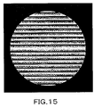
- phase distribution of the liquid crystal layer 502 which is given by the equation (4), can be illustrated as shown in FIG. 15 .
- This phase distribution can be realized by dividing the electrode into plural segments on the basis of a relatively simple pattern.
- the outward light-beam liquid crystal panel 14 and the homeward light-beam liquid crystal panel 151 are separated from each other, thus being formed into an individual panel structure.
- both the panels 14 and 151 can be laminated to each other.
- placing three or more kinds of liquid crystal layers within a single panel is able to provide the similar functions to the above.
- the positional relationship between the liquid crystal layers is not limited to that shown in FIG. 14 , but can be reversed.
- the same operations and advantages can be provided, as long as the orientation directions in the aberration-correcting two liquid layers are orthogonal to each other.
- the present embodiment provides an additional advantage that each of the electrode patterns for the liquid crystal layers is relatively simpler, due to the fact that the number of liquid layers are raised.
- FIGS. 14 , 17 and 18 a fourth embodiment of the present invention will now be described.
- the present embodiment relates to division of the homeward laser beam LB into four beams, with the aberration still corrected properly, by changing a phase pattern given to the liquid crystal panel 151 as shown in FIG. 14 .
- optical system already been used by the foregoing embodiments is also applied to the present fourth embodiment, so its detailed explanation will be omitted.
- FIG. 17 exemplifies a phase distribution given to the laser beam by the liquid crystal layer 502
- FIG. 18 exemplifies divided segments of the electrode of the liquid crystal layer 502 .
- the electrode pattern can be more simplified.
- the outward laser-beam liquid crystal panel 14 and the homeward laser-beam liquid crystal panel 151 can be laminated to each other to form a mono structure.
- placing three or more kinds of liquid crystal layers within a single panel is able to provide the similar functions to the above.
- the positional relationship between the liquid crystal layers is not limited to that shown in FIG. 14 , but can be reversed.
- the same operations and advantages can be provided, as long as the orientation directions in the aberration-correcting two liquid layers are orthogonal to each other.
- the present embodiment provides an additional advantage that each of the electrode patterns for the liquid crystal layers is relatively simpler, due to that fact that the number of liquid layers are raised.
- the aberration-correcting unit with the liquid crystal which is entitled to correct the aberration and divide the light beam, is not confined to those configurations described in the first and second embodiments.
- Such aberration-correcting unit can be applied to any kind of optical apparatus, provided that the apparatus is configured to detect a light beam reflected from an object to be detected.
Applications Claiming Priority (2)
| Application Number | Priority Date | Filing Date | Title |
|---|---|---|---|
| JPP2002-304713 | 2002-10-18 | ||
| JP2002304713A JP2004138900A (ja) | 2002-10-18 | 2002-10-18 | 収差補正素子、収差補正装置、情報記録再生装置及び収差補正方法 |
Publications (2)
| Publication Number | Publication Date |
|---|---|
| US20040170107A1 US20040170107A1 (en) | 2004-09-02 |
| US7126901B2 true US7126901B2 (en) | 2006-10-24 |
Family
ID=32452055
Family Applications (1)
| Application Number | Title | Priority Date | Filing Date |
|---|---|---|---|
| US10/686,283 Expired - Fee Related US7126901B2 (en) | 2002-10-18 | 2003-10-15 | Device and unit for correcting aberration of light beam |
Country Status (2)
| Country | Link |
|---|---|
| US (1) | US7126901B2 (ja) |
| JP (1) | JP2004138900A (ja) |
Cited By (5)
| Publication number | Priority date | Publication date | Assignee | Title |
|---|---|---|---|---|
| US20040257962A1 (en) * | 2003-06-19 | 2004-12-23 | Call/Recall Inc. | Optical storage with ultra high storage capacity |
| US20050276204A1 (en) * | 2004-06-11 | 2005-12-15 | Nec Corporation | Objective lens drive unit in an optical head |
| US20090073825A1 (en) * | 2005-04-21 | 2009-03-19 | Pioneer Corporation | Optical pick-up, aberration correcting method, optical pickup program, information recording device and method, information recording program, information reproducing device and method, information reproducing program, and information recording medium |
| US20090135685A1 (en) * | 2005-09-06 | 2009-05-28 | Pioneer Corporation | Aberration correcting apparatus and program for correcting aberration |
| US20090201785A1 (en) * | 2008-02-08 | 2009-08-13 | Masahisa Shinoda | Optical pickup and optical disc drive |
Families Citing this family (5)
| Publication number | Priority date | Publication date | Assignee | Title |
|---|---|---|---|---|
| EP1728247A1 (en) * | 2004-03-09 | 2006-12-06 | Koninklijke Philips Electronics N.V. | Optical device with polarization independent phase structure system. |
| WO2006009176A1 (ja) * | 2004-07-20 | 2006-01-26 | Asahi Glass Company, Limited | 液晶レンズ素子および光ヘッド装置 |
| KR100716990B1 (ko) | 2005-01-05 | 2007-05-14 | 삼성전자주식회사 | 수차 보정용 액정소자 및 이를 구비한 광픽업 및 광 기록및/또는 재생기기 |
| JP4792910B2 (ja) * | 2005-10-18 | 2011-10-12 | コニカミノルタホールディングス株式会社 | 液晶デバイスおよび光ピックアップ |
| US20220244530A1 (en) * | 2021-02-03 | 2022-08-04 | Kla Corporation | Correcting aberration and apodization of an optical system using correction plates |
Citations (3)
| Publication number | Priority date | Publication date | Assignee | Title |
|---|---|---|---|---|
| JPH09128785A (ja) | 1995-08-31 | 1997-05-16 | Pioneer Electron Corp | 光ピックアップ |
| US6859429B2 (en) * | 2000-05-24 | 2005-02-22 | Pioneer Corporation | Aberration correcting unit, optical pickup apparatus, and recording/reproducing apparatus |
| US7020055B2 (en) * | 2001-09-04 | 2006-03-28 | Samsung Electronics Co., Ltd. | Optical pickup apparatus |
-
2002
- 2002-10-18 JP JP2002304713A patent/JP2004138900A/ja active Pending
-
2003
- 2003-10-15 US US10/686,283 patent/US7126901B2/en not_active Expired - Fee Related
Patent Citations (3)
| Publication number | Priority date | Publication date | Assignee | Title |
|---|---|---|---|---|
| JPH09128785A (ja) | 1995-08-31 | 1997-05-16 | Pioneer Electron Corp | 光ピックアップ |
| US6859429B2 (en) * | 2000-05-24 | 2005-02-22 | Pioneer Corporation | Aberration correcting unit, optical pickup apparatus, and recording/reproducing apparatus |
| US7020055B2 (en) * | 2001-09-04 | 2006-03-28 | Samsung Electronics Co., Ltd. | Optical pickup apparatus |
Cited By (7)
| Publication number | Priority date | Publication date | Assignee | Title |
|---|---|---|---|---|
| US20040257962A1 (en) * | 2003-06-19 | 2004-12-23 | Call/Recall Inc. | Optical storage with ultra high storage capacity |
| US7436750B2 (en) * | 2003-06-19 | 2008-10-14 | Call/Recall Inc. | Optical storage with ultra high storage capacity |
| US20050276204A1 (en) * | 2004-06-11 | 2005-12-15 | Nec Corporation | Objective lens drive unit in an optical head |
| US20090073825A1 (en) * | 2005-04-21 | 2009-03-19 | Pioneer Corporation | Optical pick-up, aberration correcting method, optical pickup program, information recording device and method, information recording program, information reproducing device and method, information reproducing program, and information recording medium |
| US20090135685A1 (en) * | 2005-09-06 | 2009-05-28 | Pioneer Corporation | Aberration correcting apparatus and program for correcting aberration |
| US20090201785A1 (en) * | 2008-02-08 | 2009-08-13 | Masahisa Shinoda | Optical pickup and optical disc drive |
| US8077581B2 (en) * | 2008-02-08 | 2011-12-13 | Mitsubishi Electric Corporation | Optical pickup and optical disc drive |
Also Published As
| Publication number | Publication date |
|---|---|
| US20040170107A1 (en) | 2004-09-02 |
| JP2004138900A (ja) | 2004-05-13 |
Similar Documents
| Publication | Publication Date | Title |
|---|---|---|
| US7031038B2 (en) | Hologram apparatus capable of detecting and correcting distortion of hologram image | |
| US6707773B2 (en) | Optical head and optical information recording and playback apparatus | |
| US7542398B2 (en) | Aberration correcting element in the optical head of a recording and reproduction system using independent control of phase distribution and defocus pattern variables | |
| US7463569B2 (en) | Optical disk apparatus with a wavelength plate having a two-dimensional array of birefringent regions | |
| US6885616B2 (en) | Optical pickup apparatus and information recording and/or reproducing apparatus | |
| JP4345814B2 (ja) | 収差補正装置、収差補正方法、光ピックアップ | |
| US7126901B2 (en) | Device and unit for correcting aberration of light beam | |
| KR101011817B1 (ko) | 액정 광소자 및 광학 장치 | |
| JP2002251774A (ja) | 光ピックアップ及びその波面収差補正装置 | |
| US7596061B2 (en) | Optical disk apparatus | |
| US7428193B2 (en) | Optical pickup device and optical recording medium reproducing device | |
| US20070115767A1 (en) | Optical pickup device | |
| US20050206731A1 (en) | Aberration correction apparatus, and control apparatus, control method and control program of optical pickup | |
| US7139234B2 (en) | Optical pickup | |
| EP1160779B1 (en) | Optical pickup and optical information recording/reproducing device | |
| KR20090033080A (ko) | 광 픽업 장치, 광 기록 매체 구동 장치 및 신호의 기록/재생 방법 | |
| JP2000090479A (ja) | 液晶パネル、光ピックアップ及び情報再生装置 | |
| JP4648633B2 (ja) | 液晶光学素子及び光学装置 | |
| US20100085860A1 (en) | Optical head device, and optical information recording/reproducing device and optical information recording/reproducing method using the same | |
| JPH10143902A (ja) | 光ピックアップ装置 | |
| JP2003338075A (ja) | 情報記録再生装置 | |
| JP2005085409A (ja) | 光ピックアップ装置 | |
| KR20060013894A (ko) | 수차보정용 액정소자를 구비하는 광픽업 | |
| JP2001331966A (ja) | 光記録再生装置 |
Legal Events
| Date | Code | Title | Description |
|---|---|---|---|
| AS | Assignment |
Owner name: PIONEER CORPORATION, JAPAN Free format text: ASSIGNMENT OF ASSIGNORS INTEREST;ASSIGNORS:IWASAKI, MASAYUKI;SATO, MAKOTO;REEL/FRAME:014618/0175;SIGNING DATES FROM 20030924 TO 20030929 |
|
| FEPP | Fee payment procedure |
Free format text: PAYOR NUMBER ASSIGNED (ORIGINAL EVENT CODE: ASPN); ENTITY STATUS OF PATENT OWNER: LARGE ENTITY |
|
| REMI | Maintenance fee reminder mailed | ||
| LAPS | Lapse for failure to pay maintenance fees | ||
| STCH | Information on status: patent discontinuation |
Free format text: PATENT EXPIRED DUE TO NONPAYMENT OF MAINTENANCE FEES UNDER 37 CFR 1.362 |
|
| FP | Lapsed due to failure to pay maintenance fee |
Effective date: 20101024 |