US7108922B2 - Siloxane-based resin and interlayer insulating film formed using the same - Google Patents
Siloxane-based resin and interlayer insulating film formed using the same Download PDFInfo
- Publication number
- US7108922B2 US7108922B2 US10/768,058 US76805804A US7108922B2 US 7108922 B2 US7108922 B2 US 7108922B2 US 76805804 A US76805804 A US 76805804A US 7108922 B2 US7108922 B2 US 7108922B2
- Authority
- US
- United States
- Prior art keywords
- independently
- group
- integer
- formula
- hydrogen atom
- Prior art date
- Legal status (The legal status is an assumption and is not a legal conclusion. Google has not performed a legal analysis and makes no representation as to the accuracy of the status listed.)
- Expired - Lifetime, expires
Links
- 0 C.C.[1*][Si]1(C)CCCCO1 Chemical compound C.C.[1*][Si]1(C)CCCCO1 0.000 description 10
- WJBOWXFBFZRCRT-UHFFFAOYSA-N C.C.CO[Si](CC[Si]1(C)CCCCO1)(OC)OC Chemical compound C.C.CO[Si](CC[Si]1(C)CCCCO1)(OC)OC WJBOWXFBFZRCRT-UHFFFAOYSA-N 0.000 description 1
- ZGKUVEUHUMCSSK-UHFFFAOYSA-N C.C.C[Si]1(CC[Si](Cl)(Cl)Cl)CCCCO1 Chemical compound C.C.C[Si]1(CC[Si](Cl)(Cl)Cl)CCCCO1 ZGKUVEUHUMCSSK-UHFFFAOYSA-N 0.000 description 1
- YNHHHLLWHGTHRM-UHFFFAOYSA-N CO[Si](C)(C)C[Si](C[Si](C)(C)OC)(OC)OC Chemical compound CO[Si](C)(C)C[Si](C[Si](C)(C)OC)(OC)OC YNHHHLLWHGTHRM-UHFFFAOYSA-N 0.000 description 1
- TYNZBURHIHXDIK-UHFFFAOYSA-N CO[Si](C)(C[Si](C[Si](C)(OC)OC)(OC)OC)OC Chemical compound CO[Si](C)(C[Si](C[Si](C)(OC)OC)(OC)OC)OC TYNZBURHIHXDIK-UHFFFAOYSA-N 0.000 description 1
- JWVHPGDCFVOYMQ-UHFFFAOYSA-N CO[Si](C)(OC)O[Si](C)(OC)OC Chemical compound CO[Si](C)(OC)O[Si](C)(OC)OC JWVHPGDCFVOYMQ-UHFFFAOYSA-N 0.000 description 1
Classifications
-
- C—CHEMISTRY; METALLURGY
- C08—ORGANIC MACROMOLECULAR COMPOUNDS; THEIR PREPARATION OR CHEMICAL WORKING-UP; COMPOSITIONS BASED THEREON
- C08G—MACROMOLECULAR COMPOUNDS OBTAINED OTHERWISE THAN BY REACTIONS ONLY INVOLVING UNSATURATED CARBON-TO-CARBON BONDS
- C08G77/00—Macromolecular compounds obtained by reactions forming a linkage containing silicon with or without sulfur, nitrogen, oxygen or carbon in the main chain of the macromolecule
- C08G77/04—Polysiloxanes
- C08G77/14—Polysiloxanes containing silicon bound to oxygen-containing groups
-
- C—CHEMISTRY; METALLURGY
- C09—DYES; PAINTS; POLISHES; NATURAL RESINS; ADHESIVES; COMPOSITIONS NOT OTHERWISE PROVIDED FOR; APPLICATIONS OF MATERIALS NOT OTHERWISE PROVIDED FOR
- C09D—COATING COMPOSITIONS, e.g. PAINTS, VARNISHES OR LACQUERS; FILLING PASTES; CHEMICAL PAINT OR INK REMOVERS; INKS; CORRECTING FLUIDS; WOODSTAINS; PASTES OR SOLIDS FOR COLOURING OR PRINTING; USE OF MATERIALS THEREFOR
- C09D183/00—Coating compositions based on macromolecular compounds obtained by reactions forming in the main chain of the macromolecule a linkage containing silicon, with or without sulfur, nitrogen, oxygen, or carbon only; Coating compositions based on derivatives of such polymers
- C09D183/14—Coating compositions based on macromolecular compounds obtained by reactions forming in the main chain of the macromolecule a linkage containing silicon, with or without sulfur, nitrogen, oxygen, or carbon only; Coating compositions based on derivatives of such polymers in which at least two but not all the silicon atoms are connected by linkages other than oxygen atoms
-
- H—ELECTRICITY
- H10—SEMICONDUCTOR DEVICES; ELECTRIC SOLID-STATE DEVICES NOT OTHERWISE PROVIDED FOR
- H10P—GENERIC PROCESSES OR APPARATUS FOR THE MANUFACTURE OR TREATMENT OF DEVICES COVERED BY CLASS H10
- H10P14/00—Formation of materials, e.g. in the shape of layers or pillars
- H10P14/60—Formation of materials, e.g. in the shape of layers or pillars of insulating materials
- H10P14/63—Formation of materials, e.g. in the shape of layers or pillars of insulating materials characterised by the formation processes
- H10P14/6326—Deposition processes
- H10P14/6342—Liquid deposition, e.g. spin-coating, sol-gel techniques or spray coating
-
- H—ELECTRICITY
- H10—SEMICONDUCTOR DEVICES; ELECTRIC SOLID-STATE DEVICES NOT OTHERWISE PROVIDED FOR
- H10P—GENERIC PROCESSES OR APPARATUS FOR THE MANUFACTURE OR TREATMENT OF DEVICES COVERED BY CLASS H10
- H10P14/00—Formation of materials, e.g. in the shape of layers or pillars
- H10P14/60—Formation of materials, e.g. in the shape of layers or pillars of insulating materials
- H10P14/66—Formation of materials, e.g. in the shape of layers or pillars of insulating materials characterised by the type of materials
- H10P14/665—Porous materials
-
- H—ELECTRICITY
- H10—SEMICONDUCTOR DEVICES; ELECTRIC SOLID-STATE DEVICES NOT OTHERWISE PROVIDED FOR
- H10P—GENERIC PROCESSES OR APPARATUS FOR THE MANUFACTURE OR TREATMENT OF DEVICES COVERED BY CLASS H10
- H10P14/00—Formation of materials, e.g. in the shape of layers or pillars
- H10P14/60—Formation of materials, e.g. in the shape of layers or pillars of insulating materials
- H10P14/66—Formation of materials, e.g. in the shape of layers or pillars of insulating materials characterised by the type of materials
- H10P14/668—Formation of materials, e.g. in the shape of layers or pillars of insulating materials characterised by the type of materials the materials being characterised by the deposition precursor materials
- H10P14/6681—Formation of materials, e.g. in the shape of layers or pillars of insulating materials characterised by the type of materials the materials being characterised by the deposition precursor materials the precursor containing a compound comprising Si
- H10P14/6684—Formation of materials, e.g. in the shape of layers or pillars of insulating materials characterised by the type of materials the materials being characterised by the deposition precursor materials the precursor containing a compound comprising Si the compound comprising silicon and oxygen
- H10P14/6686—Formation of materials, e.g. in the shape of layers or pillars of insulating materials characterised by the type of materials the materials being characterised by the deposition precursor materials the precursor containing a compound comprising Si the compound comprising silicon and oxygen the compound being a molecule comprising at least one silicon-oxygen bond and the compound having hydrogen or an organic group attached to the silicon or oxygen, e.g. a siloxane
-
- H—ELECTRICITY
- H10—SEMICONDUCTOR DEVICES; ELECTRIC SOLID-STATE DEVICES NOT OTHERWISE PROVIDED FOR
- H10P—GENERIC PROCESSES OR APPARATUS FOR THE MANUFACTURE OR TREATMENT OF DEVICES COVERED BY CLASS H10
- H10P14/00—Formation of materials, e.g. in the shape of layers or pillars
- H10P14/60—Formation of materials, e.g. in the shape of layers or pillars of insulating materials
- H10P14/69—Inorganic materials
- H10P14/692—Inorganic materials composed of oxides, glassy oxides or oxide-based glasses
- H10P14/6921—Inorganic materials composed of oxides, glassy oxides or oxide-based glasses containing silicon
- H10P14/6922—Inorganic materials composed of oxides, glassy oxides or oxide-based glasses containing silicon the material containing Si, O and at least one of H, N, C, F or other non-metal elements, e.g. SiOC, SiOC:H or SiONC
-
- Y—GENERAL TAGGING OF NEW TECHNOLOGICAL DEVELOPMENTS; GENERAL TAGGING OF CROSS-SECTIONAL TECHNOLOGIES SPANNING OVER SEVERAL SECTIONS OF THE IPC; TECHNICAL SUBJECTS COVERED BY FORMER USPC CROSS-REFERENCE ART COLLECTIONS [XRACs] AND DIGESTS
- Y10—TECHNICAL SUBJECTS COVERED BY FORMER USPC
- Y10T—TECHNICAL SUBJECTS COVERED BY FORMER US CLASSIFICATION
- Y10T428/00—Stock material or miscellaneous articles
- Y10T428/31504—Composite [nonstructural laminate]
- Y10T428/31652—Of asbestos
- Y10T428/31663—As siloxane, silicone or silane
Definitions
- the present invention relates to a siloxane-based resin and an interlayer insulating film for a semiconductor device using the same. More specifically, the present invention is directed to a siloxane-based resin linked into the form of a multi-ladder and resinous film useful as an insulating film between interconnecting layers of a semiconductor device.
- Hydrogen silsesquioxanes as well as preparation methods thereof are well known in the art.
- U.S. Pat. No. 3,615,272 discloses a method of preparing a completely condensed, soluble hydrogen silsesquioxane resin, which comprises the steps of condensing trichlorosilanes in a sulfuric acid medium and washing the resulting resin with water or aqueous sulfuric acid.
- 5,010,159 discloses a method of synthesizing a soluble, condensed hydrogen silsesquioxane resin, which comprises the steps of hydrolyzing hydrosilanes in an arylsulfuric acid hydrate-containing a hydrolysis medium and contacting the resulting resin with a neutralizing agent.
- U.S. Pat. No. 6,232,424 describes a highly soluble silicon resin composition having excellent solution stability, which was prepared by hydrolyzing and polycondensing tetraalkoxysilane, organosilane and organotrialkoxysilane monomers in the presence of water and a catalyst, and their method of preparation.
- 6,000,339 discloses a silica-based compound which is useful in improving the resistance to oxygen plasma and in improving the physical properties as well as the thickness of a coating film, which can be obtained through reacting a monomer selected from the group consisting of alkoxysilane, fluorine-containing alkoxysilane and alkylalkoxysilane with a titanium- or zirconium-alkoxide compound in the presence of water and a catalyst.
- a monomer selected from the group consisting of alkoxysilane, fluorine-containing alkoxysilane and alkylalkoxysilane with a titanium- or zirconium-alkoxide compound in the presence of water and a catalyst.
- a feature of the present invention is to provide a siloxane-based resin linked into the structure of a multi-ladder having excellent solubility and flowability as well as good mechanical properties.
- Another feature of the present invention is to provide a low dielectric insulating film using the siloxane-based resin.
- a siloxane-based resin that is prepared by hydrolyzing and condensing a silane-based monomer represented by Formula 1, selectively mixed with at least one monomer selected from the group consisting of the compounds represented by Formulae 2 to 6, in organic solvent in the presence of an acid or alkaline catalyst and water:
- composition for forming a semiconductor interlayer insulating film there is provided a composition for forming a semiconductor interlayer insulating film.
- a method of forming a semiconductor interlayer insulating film comprising the steps of:
- a semiconductor interlayer insulating film containing the siloxane-based resin of the present invention is provided.
- a multi-crosslinkable siloxane monomer used in the present invention has a structure in which the silicon atom is linked by a carbon atom, and the silicon atom has at least one hydrolysable functional group.
- the structure is represented by Formula 1:
- a linear or a cyclic siloxane monomer may be further added.
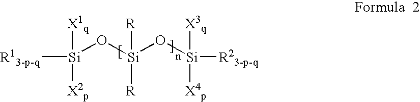
- the linear siloxane monomer has a linear structure in which a silicon atom and at least one hydrolyzable group is contained in the terminal part of the monomer. It is represented by Formula 2:
- the cyclic siloxane monomer has a cyclic structure, in which a silicon atom and at least one hydrolyzable group is present. It is represented by Formula 3:
- silane compounds having at least two hydroyzable functional groups may be used.
- the silane compounds are represented by Formulae 4 to 6: SiX 1 X 2 X 3 X 4 Formula 4 R 1 SiX 1 X 2 X 3 Formula 5 R 1 R 2 SiX 1 X 2 Formula 6 wherein,
- Siloxane-based resins according to the present invention are prepared by hydrolyzing and condensing the monomer of Formula 1, selectively mixed with at least one monomer selected from the group consisting of the compounds of Formulas 2 to 6, in an organic solvent in the presence of an acid or alkaline catalyst and water.
- the multi-ladder type siloxane resin may be represented by the following Formula 7:
- the above high molecule is in a ladder-form, in which a silicon atom is linked with two carbon atoms and two oxygen atoms, and exhibits the properties of a linear siloxane high molecule and a network siloxane high molecule.
- the multi-ladder type siloxane-based resin has excellent solubility and flowability as the linear siloxane high molecules as well as the good rigidity of the siloxane main chain, as the network siloxane high molecule.
- the multi-ladder type siloxane-based resin can be used not only as an insulator film but also as a material with high rigidity in the field of existing siloxane-based high molecules.
- the monomer of Formula 1 and the monomer selected from the group consisting of the compounds represented by Formulas 2 to 6 are mixed in a molar ratio of 1:99 to 99:1.
- an acid catalyst for the preparation of the inventive siloxane-based resin hydrochloric acid, nitric acid, benzene sulfonic acid, oxalic acid, formic acid, etc. are exemplified.
- a base catalyst potassium hydroxide, sodium hydroxide, triethylamine, sodium bicarbonate, pyridine, etc. are exemplified.
- the molar ratio of the catalyst to the monomers of formulas 1 to 6 is 0.000001:1–10:1.
- the molar ratio of water used in the preparation of the inventive siloxane-based resin to the monomers of Formulas 1 to 6 is 1:1–1000:1.
- Non-limiting examples of the organic solvent used in the preparation of the inventive siloxane-based resin include aliphatic hydrocarbon solvents such as hexane; aromatic hydrocarbon solvents such as anisole, mesitylene and xylene; ketone-based solvents such as methyl isobutyl ketone, 1-methyl-2-pyrrolidinone, cyclohexanone and acetone; ether-based solvents such as tetrahydrofuran and isopropyl ether; acetate-based solvents such as ethyl acetate, butyl acetate and propylene glycol methyl ether acetate; alcohol-based solvents such as isopropyl alcohol and butyl alcohol; amide-based solvents such as dimethylacetamide and dimethylformamide; silicon-based solvents; and a mixture thereof.
- aliphatic hydrocarbon solvents such as hexane
- aromatic hydrocarbon solvents such as anisole, mesitylene and xylene
- the hydrolysis and polycondensation reaction is carried out at a temperature of 0–200° C., preferably 50–100° C., for 0.1–100 hrs, preferably 0.5–24 hrs.
- the siloxane-based resin thus prepared has a Mw of 3,000–300,000.
- the Si—OR content in the entire terminal groups preferably amounts to 5 ⁇ 50 mol %. If the content is less than 5 mol %, the mechanical stability of the thin film deteriorates. If the content is more than 50 mol %, the storage stability of the composition deteriorates.
- the present invention also provides a composition and a method of forming an interlayer insulating film for a semiconductor device using the inventive siloxane-based resin.
- the insulating film has a low dielectric property below 3.0 and shows excellent mechanical and heat resistance properties.
- such an insulating film can be obtained by coating a silicon wafer with a solution containing the inventive siloxane-based resin and heat-curing the resulting coating film. That is, the inventive siloxane-based resin dissolved in an organic solvent is applied to a substrate. Then the organic solvent is evaporated by simple air-drying or by subjecting the substrate, at the beginning of the subsequent heat-curing step, to a vacuum condition or to mild heating at a temperature of 200° C.
- the resinous coating film is cured by heating the substrate at a temperature of 150–600° C., preferably 200–450° C., for 1–150 minutes, so as to provide an insoluble, substantially crack-free film.
- crack-free film is meant a film without any cracks that can be observed with an optical microscope at a magnification of 1000 ⁇ .
- insoluble film is meant a film that is substantially insoluble in any solvent described as being useful for dissolving the inventive siloxane-based resin.
- the combined use of a porogen with the inventive siloxane-based resin may further lower the dielectric constant of the final insulating film to 2.50 or less.
- porogen is meant any pore-generating compounds.
- an additional step of heating the resinous film over the decomposition temperature of the porogen is required so that the porogen can be decomposed.
- the porogen used in the present invention may be any of the compounds well known in the art, which can be exemplified by, but are not limited to, cyclodextrin, polycaprolactone, and derivatives thereof.
- the porogen is mixed in content of 1–70 wt %, based on a total solid content.
- Preferred organic solvents for the dissolution of the siloxane-based resin and the porogen to provide a liquid coating composition can be exemplified by, but are not limited to, aliphatic hydrocarbon solvents such as hexane; aromatic hydrocarbon solvents such as anisole, mesitylene and xylene; ketone-based solvents such as methyl isobutyl ketone, 1-methyl-2-pyrrolidinone, cyclohexanone and acetone; ether-based solvents such as tetrahydrofuran and isopropyl ether; acetate-based solvents such as ethyl acetate, butyl acetate and propylene glycol methyl ether acetate; alcohol-based solvents such as isopropyl alcohol and butyl alcohol; amide-based solvents such as dimethylacetamide and dimethylformamide; silicon-based solvents; and a mixture thereof.
- aliphatic hydrocarbon solvents such as hexane
- the organic solvent should be used in an amount sufficient to apply the solid components including the siloxane-based resin and the porogen evenly to the surface of a wafer.
- the organic solvent should amount to 5–70 wt % of the total composition comprising said siloxane-based resin, porogen and organic solvent. If the organic solvent content of the liquid coating composition is less than 5 wt %, part of the siloxane-based resin remains undissolved. On the other hand, if the organic solvent content is more than 50 wt %, the final resinous film is as thin as 1000 ⁇ or less.
- the liquid coating composition thus prepared can be applied to a silicon wafer according to various coating methods well known in the art.
- Non-limiting examples of the coating method useful in the present invention include spin-coating, dip-coating, spray-coating, flow-coating and screen-printing, while spin-coating is most preferred.
- Monomer (B) of 2,4,4,6-tetramethoxy-2,2,6,6-tetramethyl-2,4,6-trissilaheptane and Monomer(C) of 2,2,4,4,6,6-hexamethoxy-2,6-dimethyl-2,4,6-trissilaheptane are purchased from SII. Co, Rep. Of Korea, is used (Pat. No. 5,075,477).
- Monomer(D) of trimethoxysilane and monomer(E) of tetramethoxydimethylsiloxane are purchased from Sigma. Aldrich Co., USA, is used.
- the monomer is placed into a flask in an amount designated in Table 1, and diluted with tetrahydrofuran 15 times as much as the total amounts of the monomers in the flask. Then, the flask is cooled to ⁇ 78° C. At ⁇ 78° C., hydrochloric acid (HCl) and water are added to the flask in an amount designated in Table 1, after which the reaction temperature is gradually elevated to 70° C. The reaction is continued at 70° C. for 20 hours. At the completion of the reaction, the reaction mixture is transferred to a separatory funnel, followed by addition of diethylether and tetrahydrofuran as much as the tetrahydrofuran used in the previous dilution of the monomer.
- HCl hydrochloric acid
- Si—OH (%) Si—OCH 3 (%) Si—CH 3 (%) Si—H (%) (a) 18.3 0.0 81.7 0.0 (b) 9.9 0.0 60.5 29.6 (c) 0.0 0.0 80.5 19.5 (d) 28.6 1.1 70.3 0.0 (e) 32.2 0.8 66.7 0.0 (f) 35.6 1.0 63.4 0.0 (g) 23.3 0.7 76.0 0.0 (h) 30.7 2.3 67.0 0.0 (i) 33.5 1.0 65.5 0.0 (j) 25.7 0.0 74.3 0.0 (k) 23.7 0.3 76.4 0.0 (l) 19.5 0.5 80.0 0.0 Note: Si—OH content, Si—OCH 3 content, and Si—CH 3 content were analyzed by use of a nuclear magnetic resonance analyzer(Bruker Co.), and calculated from the following equations: Si—OH(%) Area(Si—OH) ⁇ [Ares(Si—H) + Area(Si—OH) + Area(Si—OCH 3
- the siloxane-based resins obtained from the above Example 2, and heptakis(2,3,6-tri-O-methoxy)- ⁇ -cyclodextrin are dissolved in propylene glycol methyl ether acetate (PGMEA), respectively, so that final concentration of the solid matter in the resulting liquid coating compositions is 25 wt %.
- PMEA propylene glycol methyl ether acetate
- Each of the coating compositions is then spin-coated onto a silicon wafer for 30 seconds while maintaining the spin rate of 3,000 rpm.
- the coated wafers are subjected to the sequential soft baking on a hot plate (1 min at 100° C. and another minute at 250° C.) so as to sufficiently evaporate the organic solvent. Thereafter, the temperature is elevated to 420° C. at a rate of 3° C./min under vacuum condition, at which temperature the coating films are allowed to cure for 1 hr to produce test pieces.
- Each of the test pieces thus prepared is analyzed for film thickness and refractive index.
- the film thickness and the refractive index are measured at 5 different points every test piece by the use of a profiler and a prism coupler, respectively.
- the mean thickness and refractive index are set forth in Table 3 along with their uniformity.
- P-type silicon wafers doped with boron are coated with 3000 ⁇ of thermally-oxidized silicon film, followed by sequential deposition of 100 ⁇ of titanium layer, 2000 ⁇ of aluminum layer and 100 ⁇ of titanium layer using a metal evaporator.
- a resinous film On the surface of each of these wafers is formed a resinous film in the same manner as in the above Example 4.
- a circular electrode of Im diameter which consists of a 100 ⁇ -thick titanium layer and a 5000 ⁇ -thick aluminum layer through a hard mask so as to provide a test piece having a MIM (metal-insulator-metal) structure.
- Test pieces thus prepared are subjected to measurement of capacitance at 100 kHz using PRECISION LCR METER(HP4284A) with Micromanipulator 6200 probe station.
- Test pieces prepared as in the above Example 4 are analyzed for hardness and elastic modulus using Nanoindenter II(MTS Co.). The resinous film of each test piece is indented until the indentation depth reached 10% of its whole thickness. At this time, to secure the reliability of this measurement, 6 points is indented every test piece, and mean hardness and modulus are taken. The results are set forth in Table 5.
Landscapes
- Chemical & Material Sciences (AREA)
- Chemical Kinetics & Catalysis (AREA)
- Organic Chemistry (AREA)
- Engineering & Computer Science (AREA)
- Materials Engineering (AREA)
- Wood Science & Technology (AREA)
- Life Sciences & Earth Sciences (AREA)
- Health & Medical Sciences (AREA)
- Medicinal Chemistry (AREA)
- Polymers & Plastics (AREA)
- Silicon Polymers (AREA)
- Formation Of Insulating Films (AREA)
- Compositions Of Macromolecular Compounds (AREA)
Abstract
Description

wherein,
-
- R1 and R2 are independently a hydrogen atom, a C1–C3 alkyl group, a C3–C10 cycloalkyl group or a C6–C15 aryl group;
- X1, X2, X3, X4, X5, and X6 are independently a halogen atom or a C1–C5 alkoxy group;
- m is an integer of 1–5;
- n is an integer of 1–3; and
- p and q are independently an integer of 0–1,
wherein,
-
- R1, R2 and R are independently a hydrogen atom, a C1–C3 alkyl group, a C3–C10 cycloalkyl group or a C6–C15 aryl group;
- X1, X2, X3 and X4 are independently a halogen atom or a C1–C5 alkoxy group;
- n is an integer of 1–3; and
- p and q are independently an integer of 0–1,

wherein,
-
- R1 and R2 are independently a hydrogen atom, a C1–C3 alkyl group, a C3–C10 cycloalkyl group or a C6–C15 aryl group;
- Xs is a halogen atom, or a C1–C5 alkoxy group;
- r is an integer of 0–10;
- s is an integer of 1–3; and
- t is an integer of 3–8,
SiX1X2X3X4 Formula 4
R1SiX1X2X3, and Formula 5
R1R2SiX1X2 Formula 6
wherein, - R1 and R2 are independently a hydrogen atom, a C1–C3 alkyl group, a C3–C10 cycloalkyl group or a C6–C15 aryl group; and
- X1, X2, X3 and X4 are independently a halogen atom or a C1–C5 alkoxy group.
-
- providing a resin solution by dissolving the siloxane-based resin in an organic solvent; and
- coating a silicon wafer with the resin solution; and
- heat-curing the resulting coating film.

wherein,
-
- R1 and R2 are independently a hydrogen atom, a C1–C3 alkyl group, a C3–C10 cycloalkyl group or a C6–C15 aryl group;
- X1, X2, X3, X4, X5 and X6 are independently a halogen atom or a C1–C5 alkoxy group;
- m is an integer of 1–5;
- n is an integer of 1–3; and
- p and q are independently an integer of 0–1,

wherein,
-
- R1, R2 and R are independently a hydrogen atom, a C1–C3 alkyl group, a C3–C10 cycloalkyl group or a C6–C15 aryl group;
- X1, X2, X3 and X4 are independently a halogen atom or a C1–C5 alkoxy group;
- n is an integer of 1–3; and
- p and q are independently an integer of 0–1.

wherein,
-
- R1 and R2 are independently a hydrogen atom, a C1–C3 alkyl group, a C3–C10 cycloalkyl group or a C6–C15 aryl group;
- Xs is a halogen atom, or a C1–C5 alkoxy group;
- r is an integer of 0–10;
- s is an integer of 1–3; and
- t is an integer of 3–8.
SiX1X2X3X4 Formula 4
R1SiX1X2X3 Formula 5
R1R2SiX1X2 Formula 6
wherein,
-
- R1 and R2 are independently a hydrogen atom, a C1–C3 alkyl group, a C3–C10 cycloalkyl group or a C6–C15 aryl group; and
- X1, X2, X3 and X4 are independently a halogen atom or a C1–C5 alkoxy group.

wherein,
-
- X is a halogen atom, a hydroxy group or a C1-5 alkoxy group;
- R is a hydrogen atom, a C1-3 alkyl group, a C3-10 cycloalkyl group, or a C6-15 aryl group;
- l is an integer of 2–10000;
- m is an integer of 1–5; and
- n is an integer of 1–3.


H—Si(OMe)3

| TABLE 1 | ||||
| Siloxane | Monomer (mmol) | HCl | H2O | Final |
| Resin | (A) | (B) | (C) | (D) | (E) | (mmol) | (mmol) | Resin(g) |
| (a) | — | — | 39.610 | — | — | 0.238 | 663 | 4.5 |
| (b) | — | — | 24.550 | 24.550 | — | 0.221 | 616 | 4.9 |
| (c) | — | 32.733 | — | 32.733 | — | 0.229 | 639 | 5.2 |
| (d) | 8.399 | — | 19.597 | — | — | 0.218 | 609 | 6.5 |
| (e) | 8.399 | — | 8.399 | — | — | 0.151 | 422 | 5.9 |
| (f) | 11.898 | — | 5.412 | — | — | 0.175 | 488 | 6.9 |
| (g) | 8.399 | 19.597 | — | — | — | 0.179 | 500 | 6.4 |
| (h) | 8.399 | 8.399 | — | — | — | 0.134 | 375 | 5.7 |
| (i) | 11.898 | 5.142 | — | — | — | 0.164 | 459 | 6.8 |
| (j) | — | — | 30.950 | — | 13.264 | 0.239 | 667 | 4.7 |
| (k) | — | — | 22.107 | — | 22.107 | 0.221 | 617 | 4.6 |
| (l) | — | — | 13.264 | — | 30.950 | 0.203 | 567 | 5.4 |
| TABLE 2 | ||||
| Siloxane Resin | Si—OH (%) | Si—OCH3 (%) | Si—CH3 (%) | Si—H (%) |
| (a) | 18.3 | 0.0 | 81.7 | 0.0 |
| (b) | 9.9 | 0.0 | 60.5 | 29.6 |
| (c) | 0.0 | 0.0 | 80.5 | 19.5 |
| (d) | 28.6 | 1.1 | 70.3 | 0.0 |
| (e) | 32.2 | 0.8 | 66.7 | 0.0 |
| (f) | 35.6 | 1.0 | 63.4 | 0.0 |
| (g) | 23.3 | 0.7 | 76.0 | 0.0 |
| (h) | 30.7 | 2.3 | 67.0 | 0.0 |
| (i) | 33.5 | 1.0 | 65.5 | 0.0 |
| (j) | 25.7 | 0.0 | 74.3 | 0.0 |
| (k) | 23.7 | 0.3 | 76.4 | 0.0 |
| (l) | 19.5 | 0.5 | 80.0 | 0.0 |
| Note: | ||||
| Si—OH content, Si—OCH3 content, and Si—CH3 content were analyzed by use of a nuclear magnetic resonance analyzer(Bruker Co.), and calculated from the following equations: | ||||
| Si—OH(%) = Area(Si—OH) ÷ [Ares(Si—H) + Area(Si—OH) + Area(Si—OCH3)/3 + Area(Si—CH3)/3] × 100, | ||||
| Si—OCH3(%) = Area(Si—OCH3)/3 ÷ [Ares(Si—H) + Area(Si—OH) + Area(Si—OCH3)/3 + Area(Si—CH3)/3] × 100, | ||||
| Si—CH3(%) = Area(Si—CH3)/3 ÷ [Ares(Si—H) + Area(Si—OH) + Area(Si—OCH3)/3 + Area(Si—CH3)/3] × 100, and | ||||
| Si—H(%) = Ares(Si—H) ÷ [Ares(Si—H) + Area(Si—OH) + Area(Si—OCH3)/3 + Area(Si—CH3)/3] × 100. | ||||
| TABLE 3 | ||||
| Composition of resinous film | Refrac- | Uni- | Uni- | |
| Siloxane | tive | formity | formity | |||
| Siloxane | Resin | Porogen | Thick. | Index | of R.I. | of Thick. |
| Resin | (wt %) | (wt %) | (Å) | (R.I.) | (%) | (%) |
| (a) | 100 | — | 6889 | 1.4257 | 0.064 | 1.09 |
| (a) | 70 | 30 | 4725 | 1.3725 | 0.058 | 1.31 |
| (b) | 100 | — | 12648 | 1.4406 | 0.090 | 0.45 |
| (b) | 70 | 30 | 11273 | 1.3292 | 0.037 | 0.99 |
| (c) | 100 | — | 10193 | 1.4299 | 0.131 | 0.62 |
| (c) | 70 | 30 | 8983 | 1.3298 | 0.105 | 1.01 |
| (d) | 100 | — | 16142 | 1.4350 | 0.110 | 0.45 |
| (d) | 70 | 30 | 10940 | 1.3392 | 0.161 | 1.20 |
| (e) | 100 | — | 14360 | 1.4385 | 0.048 | 1.56 |
| (e) | 70 | 30 | 11397 | 1.3284 | 0.160 | 1.34 |
| (f) | 100 | — | 12767 | 1.4397 | 0.081 | 1.37 |
| (f) | 70 | 30 | 11397 | 1.3283 | 0.097 | 0.57 |
| (g) | 100 | — | 10193 | 1.4367 | 0.048 | 0.92 |
| (g) | 70 | 30 | 9126 | 1.3416 | 0.091 | 1.51 |
| (h) | 100 | — | 11225 | 1.4399 | 0.073 | 1.51 |
| (h) | 70 | 30 | 9724 | 1.3290 | 0.029 | 0.97 |
| (i) | 100 | — | 12553 | 1.4397 | 0.092 | 1.57 |
| (i) | 70 | 30 | 9950 | 1.3311 | 0.106 | 1.18 |
| (j) | 100 | — | 8270 | 1.4129 | 0.031 | 0.22 |
| (j) | 70 | 30 | 5914 | 1.3729 | 0.087 | 0.77 |
| (k) | 100 | — | 8206 | 1.4051 | 0.101 | 1.91 |
| (k) | 70 | 30 | 6089 | 1.3577 | 0.039 | 1.87 |
| (l) | 100 | — | 7071 | 1.3977 | 0.067 | 1.31 |
| (l) | 70 | 30 | 5564 | 1.3250 | 0.080 | 0.14 |
k=C×d/∈ o ×A
-
- wherein,
- k: dielectric constant
- C: capacitance
- ∈o: dielectric constant in vacuum
- d: the thickness of low dielectric film
- A: the contact area of electrode
| TABLE 4 | |
| Thin Film Composition | |
| Siloxane | |||
| Resin | Siloxane Resin (wt %) | Porogen (wt %) | Dielectric Constant |
| (a) | 100 | — | 2.72 |
| (a) | 70 | 30 | 2.53 |
| (b) | 100 | — | 2.59 |
| (b) | 70 | 30 | 2.18 |
| (c) | 100 | — | 2.75 |
| (c) | 70 | 30 | 2.23 |
| (d) | 100 | — | 2.70 |
| (d) | 70 | 30 | 2.20 |
| (e) | 100 | — | 2.66 |
| (e) | 70 | 30 | 2.19 |
| (f) | 100 | — | 2.73 |
| (f) | 70 | 30 | 2.16 |
| (g) | 100 | — | 2.70 |
| (g) | 70 | 30 | 2.20 |
| (h) | 100 | — | 2.65 |
| (h) | 70 | 30 | 2.15 |
| (i) | 100 | — | 2.60 |
| (i) | 70 | 30 | 2.14 |
| (j) | 100 | — | 2.72 |
| (j) | 70 | 30 | 2.42 |
| (k) | 100 | — | 2.76 |
| (k) | 70 | 30 | 2.33 |
| (l) | 100 | — | 2.71 |
| (l) | 70 | 30 | 2.26 |
| TABLE 5 | |
| Thin Film Composition | |
| Siloxane | Siloxane | Hardness | Modulus | |
| Resin | Resin (wt %) | Porogen (wt %) | (GPa) | (GPa) |
| (a) | 100 | — | 0.43 | 4.77 |
| (a) | 70 | 30 | 0.27 | 4.10 |
| (b) | 100 | — | 1.08 | 7.00 |
| (b) | 70 | 30 | 0.58 | 4.20 |
| (c) | 100 | — | 0.94 | 6.55 |
| (c) | 70 | 30 | 0.51 | 4.00 |
| (d) | 100 | — | 1.04 | 6.53 |
| (d) | 70 | 30 | 0.51 | 3.62 |
| (e) | 100 | — | 0.98 | 7.01 |
| (e) | 70 | 30 | 0.50 | 3.80 |
| (f) | 100 | — | 1.12 | 7.34 |
| (f) | 70 | 30 | 0.59 | 3.91 |
| (g) | 100 | — | 0.71 | 5.10 |
| (g) | 70 | 30 | 0.38 | 2.93 |
| (h) | 100 | — | 0.46 | 5.52 |
| (h) | 70 | 30 | 0.45 | 3.01 |
| (i) | 100 | — | 0.44 | 5.23 |
| (i) | 70 | 30 | 0.31 | 2.97 |
| (j) | 100 | — | 0.49 | 4.44 |
| (j) | 70 | 30 | 0.27 | 3.53 |
| (k) | 100 | — | 0.52 | 5.01 |
| (k) | 70 | 30 | 0.34 | 3.61 |
| (l) | 100 | — | 0.61 | 5.53 |
| (l) | 70 | 30 | 0.39 | 3.81 |
Claims (10)


SiX1X2X3X4 Formula 4
R1SiX1X2X3 Formula 5
R1R2SiX1X2 Formula 6


SiX1X2X3X4 Formula 4
R1SiX1X2X3 Formula 5
R1R2SiX1X2 Formula 6


SiX1X2X3X4 Formula 4
R1SiX1X2X3 Formula 5
R1R2SiX1X2 Formula 6


SiX1X2X3X4 Formula 4
R1SiX1X2X3 Formula 5
R1R2SiX1X2 Formula 6


SiX1X2X3X4 Formula 4
R1SiX1X2X3 Formula 5
R1R2SiX1X2 Formula 6
Applications Claiming Priority (2)
| Application Number | Priority Date | Filing Date | Title |
|---|---|---|---|
| KR1020030060811A KR20050024721A (en) | 2003-09-01 | 2003-09-01 | Novel Siloxane Polymer and a Composition for preparing Dielectric Film by using the Same |
| KR2003-60811 | 2003-09-01 |
Publications (2)
| Publication Number | Publication Date |
|---|---|
| US20050049382A1 US20050049382A1 (en) | 2005-03-03 |
| US7108922B2 true US7108922B2 (en) | 2006-09-19 |
Family
ID=36580445
Family Applications (1)
| Application Number | Title | Priority Date | Filing Date |
|---|---|---|---|
| US10/768,058 Expired - Lifetime US7108922B2 (en) | 2003-09-01 | 2004-02-02 | Siloxane-based resin and interlayer insulating film formed using the same |
Country Status (6)
| Country | Link |
|---|---|
| US (1) | US7108922B2 (en) |
| EP (1) | EP1510537B1 (en) |
| JP (1) | JP4549781B2 (en) |
| KR (1) | KR20050024721A (en) |
| CN (1) | CN100455619C (en) |
| DE (1) | DE602004000964T2 (en) |
Cited By (6)
| Publication number | Priority date | Publication date | Assignee | Title |
|---|---|---|---|---|
| US20070173401A1 (en) * | 2004-09-22 | 2007-07-26 | Landskron Kai M M | High organic group content-periodic mesoporous organosilicas (HO-PMO's) |
| US20080241748A1 (en) * | 2007-03-30 | 2008-10-02 | Shahrokh Motallebi | Etch-resistant disilane and saturated hydrocarbon bridged silicon-containing polymers, method of making the same, and method of using the same |
| US20100168327A1 (en) * | 2004-02-26 | 2010-07-01 | Jsr Corporation | Polymer and process for producing the same, composition for forming insulating film, and insulating film and method of forming the same |
| US9362030B2 (en) | 2013-08-08 | 2016-06-07 | Cheil Industries, Inc. | Composition for forming silica based insulating layer, silica based insulating layer and method for manufacturing silica based insulating layer |
| US10973908B1 (en) | 2020-05-14 | 2021-04-13 | David Gordon Bermudes | Expression of SARS-CoV-2 spike protein receptor binding domain in attenuated salmonella as a vaccine |
| US12537071B1 (en) | 2020-07-22 | 2026-01-27 | David Gordon Bermudes | Bacteria having boolean control pathways expressing therapeutic proteins including immunotherapeutic cytotoxins |
Families Citing this family (16)
| Publication number | Priority date | Publication date | Assignee | Title |
|---|---|---|---|---|
| JP4092220B2 (en) * | 2003-01-31 | 2008-05-28 | Necエレクトロニクス株式会社 | Semiconductor device and manufacturing method thereof |
| JP5110243B2 (en) * | 2004-01-16 | 2012-12-26 | Jsr株式会社 | Method for producing polymer |
| WO2005068540A1 (en) * | 2004-01-16 | 2005-07-28 | Jsr Corporation | Composition for forming insulating film, method for producing same, silica insulating film and method for forming same |
| JP2005272816A (en) * | 2004-02-26 | 2005-10-06 | Jsr Corp | POLYMER AND METHOD FOR PRODUCING SAME, COMPOSITION FOR FORMING INSULATING FILM, AND INSULATING FILM AND METHOD FOR FORMING THE SAME |
| JP5110238B2 (en) * | 2004-05-11 | 2012-12-26 | Jsr株式会社 | Insulating film forming composition and method for producing the same, and silica-based insulating film and method for forming the same |
| JP5110239B2 (en) | 2004-05-11 | 2012-12-26 | Jsr株式会社 | Method for forming organic silica film, composition for film formation |
| KR101140535B1 (en) * | 2004-05-11 | 2012-05-02 | 제이에스알 가부시끼가이샤 | Method for forming organic silica film, organic silica film, wiring structure, semiconductor device, and composition for film formation |
| EP1925024B1 (en) * | 2005-09-01 | 2012-01-25 | Freescale Semiconductor, Inc. | Capping layer formation onto a dual damescene interconnect |
| WO2007087831A1 (en) * | 2006-02-03 | 2007-08-09 | Freescale Semiconductor, Inc. | 'universal' barrier cmp slurry for use with low dielectric constant interlayer dielectrics |
| US20090301867A1 (en) * | 2006-02-24 | 2009-12-10 | Citibank N.A. | Integrated system for semiconductor substrate processing using liquid phase metal deposition |
| JPWO2008096656A1 (en) * | 2007-02-07 | 2010-05-20 | Jsr株式会社 | Silicon-containing polymer and method for synthesizing the same, film-forming composition, and silica-based film and method for forming the same |
| US8329849B2 (en) | 2008-05-16 | 2012-12-11 | Nec Corporation | Organic silicon compound and material for forming silica-based fine particle |
| KR101290260B1 (en) * | 2011-07-15 | 2013-07-26 | 주식회사 케이씨씨 | Alkali soluble silicone resin, silicone resin composition comprising the same and preparation method thereof |
| KR101393695B1 (en) * | 2012-03-14 | 2014-05-13 | 명지대학교 산학협력단 | Insulating film material for semiconductor device and method for preparing insulating film using the same |
| US10316216B2 (en) * | 2016-08-31 | 2019-06-11 | Samsung Sdi Co., Ltd. | Composition for forming silica layer, and silica layer |
| CN115449291B (en) * | 2021-06-09 | 2023-07-07 | 荣耀终端有限公司 | Waterproof and insulating coating and its application |
Citations (14)
| Publication number | Priority date | Publication date | Assignee | Title |
|---|---|---|---|---|
| US2590937A (en) * | 1950-05-01 | 1952-04-01 | Dow Corning | Organosilicon resins |
| US3615272A (en) | 1968-11-04 | 1971-10-26 | Dow Corning | Condensed soluble hydrogensilsesquioxane resin |
| US4399266A (en) | 1980-08-26 | 1983-08-16 | Japan Synthetic Rubber Co., Ltd. | Laddery lower alkylpolysilsesquioxane having heat-resistant thin film-formability and process for preparing same |
| US4756977A (en) | 1986-12-03 | 1988-07-12 | Dow Corning Corporation | Multilayer ceramics from hydrogen silsesquioxane |
| US4999397A (en) | 1989-07-28 | 1991-03-12 | Dow Corning Corporation | Metastable silane hydrolyzates and process for their preparation |
| US5010159A (en) | 1989-09-01 | 1991-04-23 | Dow Corning Corporation | Process for the synthesis of soluble, condensed hydridosilicon resins containing low levels of silanol |
| US5138080A (en) * | 1991-02-25 | 1992-08-11 | Korea Institute Of Science And Technology | Polysilamethylenosilanes and process for their preparation |
| US5302734A (en) * | 1991-06-14 | 1994-04-12 | Korea Institute Of Science And Technology | 1,3-disilacyclobutanes and the method for producing thereof |
| US5853808A (en) | 1995-09-12 | 1998-12-29 | Gelest Inc. | Method of using siloxane polymers |
| US6000339A (en) | 1994-06-30 | 1999-12-14 | Hitachi Chemical Company, Ltd. | Material for forming silica-base coated insulation film, process for producing the material, silica-base insulation film, semiconductor device, and process for producing the device |
| EP0997497A1 (en) | 1997-07-15 | 2000-05-03 | Asahi Kasei Kogyo Kabushiki Kaisha | Alkoxysilane/organic polymer composition for thin insulating film production and use thereof |
| US6087521A (en) * | 1999-05-17 | 2000-07-11 | Jung; Il Nam | Silicon compounds containing silamethylene bonds and method for their preparation |
| US6232424B1 (en) | 1999-12-13 | 2001-05-15 | Dow Corning Corporation | Soluble silicone resin compositions having good solution stability |
| KR20030060811A (en) | 2002-01-09 | 2003-07-16 | 세이코 엡슨 가부시키가이샤 | Electronic circuit, electroluminescent display device, electro-optical device, electronic apparatus, method of controlling the current supply to an organic electroluminescent pixel, and method for driving a circuit |
Family Cites Families (24)
| Publication number | Priority date | Publication date | Assignee | Title |
|---|---|---|---|---|
| GB1043144A (en) * | 1963-09-18 | 1966-09-21 | Ici Ltd | Disilmethylenes and siloxanes prepared therefrom |
| JPS58171416A (en) * | 1982-04-02 | 1983-10-08 | Hitachi Ltd | heat resistant polymer |
| JPS6169836A (en) * | 1984-09-12 | 1986-04-10 | Chisso Corp | Stepladder polymer containing silicon atoms and production thereof |
| JPH0791308B2 (en) * | 1989-06-20 | 1995-10-04 | 信越化学工業株式会社 | Trialkylsilylmethyl group-containing silane compound |
| JP2527379B2 (en) * | 1990-06-26 | 1996-08-21 | 信越化学工業株式会社 | Primer composition |
| KR940007416B1 (en) * | 1991-01-22 | 1994-08-18 | Korea Inst Sci & Tech | Process for the preparation of silaalkane |
| JP2795135B2 (en) * | 1993-06-07 | 1998-09-10 | 信越化学工業株式会社 | Method for producing organoalkoxysilane compound |
| JPH0812762A (en) * | 1994-06-29 | 1996-01-16 | Toray Dow Corning Silicone Co Ltd | Fluoroorganosilicon polymer and its production |
| JPH08217879A (en) * | 1995-02-15 | 1996-08-27 | Mitsubishi Rayon Co Ltd | Heat resistant resin and method for producing the same |
| JPH11209474A (en) * | 1998-01-19 | 1999-08-03 | Shin Etsu Chem Co Ltd | Method for producing silicon-based polymer compound |
| JPH11322992A (en) * | 1998-05-18 | 1999-11-26 | Jsr Corp | Porous membrane |
| JP2000038545A (en) * | 1998-05-18 | 2000-02-08 | Jsr Corp | Composition for forming film, method for forming film, and low-density film |
| US6225238B1 (en) * | 1999-06-07 | 2001-05-01 | Allied Signal Inc | Low dielectric constant polyorganosilicon coatings generated from polycarbosilanes |
| JP2001040283A (en) * | 1999-07-29 | 2001-02-13 | Jsr Corp | Method for producing film-forming composition, film-forming composition and insulating film-forming material |
| TR200200411T2 (en) * | 1999-08-20 | 2002-06-21 | Bayer Aktiengesellschaft | The inorganic coating composition, a process for its manufacture, use, and a non-stick coating thus obtained. |
| US6492480B1 (en) * | 1999-10-28 | 2002-12-10 | Japan Science And Technology Corporation | Method of polymerizing a silalkylenesiloxane |
| DE10031764A1 (en) * | 2000-06-29 | 2002-01-10 | Bayer Ag | Process for the production of sol-gel compositions with reduced solvent content and improved storage stability and their use |
| KR100382702B1 (en) * | 2000-09-18 | 2003-05-09 | 주식회사 엘지화학 | Method for preparing organic silicate polymer |
| KR100343938B1 (en) * | 2000-11-29 | 2002-07-20 | Samsung Electronics Co Ltd | Preparation method of interlayer insulation membrane of semiconductor |
| EP1245628B1 (en) * | 2001-03-27 | 2008-08-27 | Samsung Electronics Co., Ltd. | Composition for preparing substances having nano-pores |
| DE60204502T2 (en) * | 2001-03-27 | 2006-05-18 | Samsung Electronics Co., Ltd., Suwon | Polysiloxane resin and process for producing an intermediate layer thereof for wafers |
| TW200303846A (en) * | 2002-02-06 | 2003-09-16 | Asahi Chemical Ind | Coating compositions for forming insulating thin films |
| WO2003087228A1 (en) * | 2002-04-12 | 2003-10-23 | Clariant International Ltd. | Composition of silicon-containing copolymer, solvent-soluble crosslinked silicon-containing copolymer, and cured articles obtained therefrom |
| KR100507967B1 (en) * | 2003-07-01 | 2005-08-10 | 삼성전자주식회사 | Siloxane-based Resin and Semiconductive Interlayer Insulating Film Using the Same |
-
2003
- 2003-09-01 KR KR1020030060811A patent/KR20050024721A/en not_active Abandoned
-
2004
- 2004-02-02 US US10/768,058 patent/US7108922B2/en not_active Expired - Lifetime
- 2004-08-20 DE DE200460000964 patent/DE602004000964T2/en not_active Expired - Lifetime
- 2004-08-20 EP EP20040255029 patent/EP1510537B1/en not_active Expired - Lifetime
- 2004-08-30 JP JP2004250188A patent/JP4549781B2/en not_active Expired - Lifetime
- 2004-08-30 CN CNB2004100748860A patent/CN100455619C/en not_active Expired - Fee Related
Patent Citations (14)
| Publication number | Priority date | Publication date | Assignee | Title |
|---|---|---|---|---|
| US2590937A (en) * | 1950-05-01 | 1952-04-01 | Dow Corning | Organosilicon resins |
| US3615272A (en) | 1968-11-04 | 1971-10-26 | Dow Corning | Condensed soluble hydrogensilsesquioxane resin |
| US4399266A (en) | 1980-08-26 | 1983-08-16 | Japan Synthetic Rubber Co., Ltd. | Laddery lower alkylpolysilsesquioxane having heat-resistant thin film-formability and process for preparing same |
| US4756977A (en) | 1986-12-03 | 1988-07-12 | Dow Corning Corporation | Multilayer ceramics from hydrogen silsesquioxane |
| US4999397A (en) | 1989-07-28 | 1991-03-12 | Dow Corning Corporation | Metastable silane hydrolyzates and process for their preparation |
| US5010159A (en) | 1989-09-01 | 1991-04-23 | Dow Corning Corporation | Process for the synthesis of soluble, condensed hydridosilicon resins containing low levels of silanol |
| US5138080A (en) * | 1991-02-25 | 1992-08-11 | Korea Institute Of Science And Technology | Polysilamethylenosilanes and process for their preparation |
| US5302734A (en) * | 1991-06-14 | 1994-04-12 | Korea Institute Of Science And Technology | 1,3-disilacyclobutanes and the method for producing thereof |
| US6000339A (en) | 1994-06-30 | 1999-12-14 | Hitachi Chemical Company, Ltd. | Material for forming silica-base coated insulation film, process for producing the material, silica-base insulation film, semiconductor device, and process for producing the device |
| US5853808A (en) | 1995-09-12 | 1998-12-29 | Gelest Inc. | Method of using siloxane polymers |
| EP0997497A1 (en) | 1997-07-15 | 2000-05-03 | Asahi Kasei Kogyo Kabushiki Kaisha | Alkoxysilane/organic polymer composition for thin insulating film production and use thereof |
| US6087521A (en) * | 1999-05-17 | 2000-07-11 | Jung; Il Nam | Silicon compounds containing silamethylene bonds and method for their preparation |
| US6232424B1 (en) | 1999-12-13 | 2001-05-15 | Dow Corning Corporation | Soluble silicone resin compositions having good solution stability |
| KR20030060811A (en) | 2002-01-09 | 2003-07-16 | 세이코 엡슨 가부시키가이샤 | Electronic circuit, electroluminescent display device, electro-optical device, electronic apparatus, method of controlling the current supply to an organic electroluminescent pixel, and method for driving a circuit |
Non-Patent Citations (2)
| Title |
|---|
| Abstract JP 05093073, Apr. 16, 1993. * |
| Abstract, KR 9507335, Jul. 10, 1992. * |
Cited By (10)
| Publication number | Priority date | Publication date | Assignee | Title |
|---|---|---|---|---|
| US20100168327A1 (en) * | 2004-02-26 | 2010-07-01 | Jsr Corporation | Polymer and process for producing the same, composition for forming insulating film, and insulating film and method of forming the same |
| US8404786B2 (en) * | 2004-02-26 | 2013-03-26 | Jsr Corporation | Polymer and process for producing the same, composition for forming insulating film, and insulating film and method of forming the same |
| US20070173401A1 (en) * | 2004-09-22 | 2007-07-26 | Landskron Kai M M | High organic group content-periodic mesoporous organosilicas (HO-PMO's) |
| US7947799B2 (en) * | 2004-09-22 | 2011-05-24 | Kai Manfred Martin Landskron | High organic group content-periodic mesoporous organosilicas (HO-PMO's) |
| US20080241748A1 (en) * | 2007-03-30 | 2008-10-02 | Shahrokh Motallebi | Etch-resistant disilane and saturated hydrocarbon bridged silicon-containing polymers, method of making the same, and method of using the same |
| US8026035B2 (en) | 2007-03-30 | 2011-09-27 | Cheil Industries, Inc. | Etch-resistant disilane and saturated hydrocarbon bridged silicon-containing polymers, method of making the same, and method of using the same |
| US9362030B2 (en) | 2013-08-08 | 2016-06-07 | Cheil Industries, Inc. | Composition for forming silica based insulating layer, silica based insulating layer and method for manufacturing silica based insulating layer |
| US10973908B1 (en) | 2020-05-14 | 2021-04-13 | David Gordon Bermudes | Expression of SARS-CoV-2 spike protein receptor binding domain in attenuated salmonella as a vaccine |
| US11406702B1 (en) | 2020-05-14 | 2022-08-09 | David Gordon Bermudes | Expression of SARS-CoV-2 spike protein receptor binding domain in attenuated Salmonella as a vaccine |
| US12537071B1 (en) | 2020-07-22 | 2026-01-27 | David Gordon Bermudes | Bacteria having boolean control pathways expressing therapeutic proteins including immunotherapeutic cytotoxins |
Also Published As
| Publication number | Publication date |
|---|---|
| JP2005076031A (en) | 2005-03-24 |
| EP1510537A1 (en) | 2005-03-02 |
| DE602004000964T2 (en) | 2007-01-18 |
| KR20050024721A (en) | 2005-03-11 |
| EP1510537B1 (en) | 2006-05-24 |
| DE602004000964D1 (en) | 2006-06-29 |
| US20050049382A1 (en) | 2005-03-03 |
| JP4549781B2 (en) | 2010-09-22 |
| CN100455619C (en) | 2009-01-28 |
| CN1597738A (en) | 2005-03-23 |
Similar Documents
| Publication | Publication Date | Title |
|---|---|---|
| US7108922B2 (en) | Siloxane-based resin and interlayer insulating film formed using the same | |
| US7374820B2 (en) | Siloxane-based resin containing germanium and an interlayer insulating film for a semiconductor device using the same | |
| US8053173B2 (en) | Multi-functional linear siloxane compound, a siloxane polymer prepared from the compound, and a process for forming a dielectric film by using the polymer | |
| EP1245642B1 (en) | Siloxane-based resin and method for forming an insulating film between interconnecting layers in wafers | |
| US6623711B2 (en) | Siloxane-based resin and method for forming insulating film between interconnect layers in semiconductor devices by using the same | |
| US7071540B2 (en) | Siloxane-based resin and a semiconductor interlayer insulating film using the same | |
| US20090130862A1 (en) | Multi-functional cyclic silicate compound, siloxane-based polymer prepared from the compound and process of producing insulating film using the polymer | |
| US7470634B2 (en) | Method for forming interlayer dielectric film for semiconductor device by using polyhedral molecular silsesquioxane | |
| US7014917B2 (en) | Siloxane-based resin and interlayer insulating film for a semiconductor device made using the same | |
| US6908977B2 (en) | Siloxane-based resin and method of forming an insulating film between interconnect layers of a semiconductor device using the same | |
| US20060134441A1 (en) | Siloxane-based polymer and method for forming dielectric film using the polymer | |
| KR100475548B1 (en) | Siloxane-based resin and method for forming insulating film between metal layers in semiconductor using the same |
Legal Events
| Date | Code | Title | Description |
|---|---|---|---|
| AS | Assignment |
Owner name: SAMSUNG ELECTRONICS CO., LTD., KOREA, REPUBLIC OF Free format text: ASSIGNMENT OF ASSIGNORS INTEREST;ASSIGNORS:LYU, YI YEOL;YIM, JIN HEONG;SONG, KI YONG;AND OTHERS;REEL/FRAME:014951/0018 Effective date: 20040202 |
|
| FEPP | Fee payment procedure |
Free format text: PAYOR NUMBER ASSIGNED (ORIGINAL EVENT CODE: ASPN); ENTITY STATUS OF PATENT OWNER: LARGE ENTITY |
|
| STCF | Information on status: patent grant |
Free format text: PATENTED CASE |
|
| FPAY | Fee payment |
Year of fee payment: 4 |
|
| FEPP | Fee payment procedure |
Free format text: PAYER NUMBER DE-ASSIGNED (ORIGINAL EVENT CODE: RMPN); ENTITY STATUS OF PATENT OWNER: LARGE ENTITY Free format text: PAYOR NUMBER ASSIGNED (ORIGINAL EVENT CODE: ASPN); ENTITY STATUS OF PATENT OWNER: LARGE ENTITY |
|
| FPAY | Fee payment |
Year of fee payment: 8 |
|
| MAFP | Maintenance fee payment |
Free format text: PAYMENT OF MAINTENANCE FEE, 12TH YEAR, LARGE ENTITY (ORIGINAL EVENT CODE: M1553) Year of fee payment: 12 |