US7106500B2 - Raman amplifier system - Google Patents
Raman amplifier system Download PDFInfo
- Publication number
- US7106500B2 US7106500B2 US10/825,120 US82512004A US7106500B2 US 7106500 B2 US7106500 B2 US 7106500B2 US 82512004 A US82512004 A US 82512004A US 7106500 B2 US7106500 B2 US 7106500B2
- Authority
- US
- United States
- Prior art keywords
- raman
- wavelength
- optical
- crystalline material
- amplifier system
- Prior art date
- Legal status (The legal status is an assumption and is not a legal conclusion. Google has not performed a legal analysis and makes no representation as to the accuracy of the status listed.)
- Expired - Lifetime, expires
Links
- 238000001069 Raman spectroscopy Methods 0.000 title claims abstract description 47
- 230000003287 optical effect Effects 0.000 claims abstract description 55
- 239000002178 crystalline material Substances 0.000 claims abstract description 19
- 239000004065 semiconductor Substances 0.000 claims description 14
- 230000003321 amplification Effects 0.000 claims description 11
- 238000003199 nucleic acid amplification method Methods 0.000 claims description 11
- 239000012212 insulator Substances 0.000 claims description 8
- 239000000463 material Substances 0.000 claims description 7
- 238000000034 method Methods 0.000 claims description 6
- 229910052710 silicon Inorganic materials 0.000 claims description 6
- 239000010703 silicon Substances 0.000 claims description 6
- 230000001902 propagating effect Effects 0.000 claims description 4
- 229910000577 Silicon-germanium Inorganic materials 0.000 claims description 2
- LEVVHYCKPQWKOP-UHFFFAOYSA-N [Si].[Ge] Chemical compound [Si].[Ge] LEVVHYCKPQWKOP-UHFFFAOYSA-N 0.000 claims description 2
- 230000007547 defect Effects 0.000 claims description 2
- ZUGYBSSWYZCQSV-UHFFFAOYSA-N indium(3+);phosphite Chemical compound [In+3].[O-]P([O-])[O-] ZUGYBSSWYZCQSV-UHFFFAOYSA-N 0.000 claims description 2
- 239000012528 membrane Substances 0.000 claims description 2
- 239000004038 photonic crystal Substances 0.000 claims description 2
- 230000003993 interaction Effects 0.000 description 6
- VYPSYNLAJGMNEJ-UHFFFAOYSA-N Silicium dioxide Chemical compound O=[Si]=O VYPSYNLAJGMNEJ-UHFFFAOYSA-N 0.000 description 4
- 238000001228 spectrum Methods 0.000 description 4
- XUIMIQQOPSSXEZ-UHFFFAOYSA-N Silicon Chemical compound [Si] XUIMIQQOPSSXEZ-UHFFFAOYSA-N 0.000 description 3
- 238000004519 manufacturing process Methods 0.000 description 3
- 229910021417 amorphous silicon Inorganic materials 0.000 description 2
- 230000005540 biological transmission Effects 0.000 description 2
- 239000012141 concentrate Substances 0.000 description 2
- 230000000694 effects Effects 0.000 description 2
- 239000000835 fiber Substances 0.000 description 2
- 238000005086 pumping Methods 0.000 description 2
- 239000000377 silicon dioxide Substances 0.000 description 2
- 238000005253 cladding Methods 0.000 description 1
- 238000004891 communication Methods 0.000 description 1
- 229910021419 crystalline silicon Inorganic materials 0.000 description 1
- 238000010586 diagram Methods 0.000 description 1
- -1 gallium-arsenite Chemical compound 0.000 description 1
- 239000013307 optical fiber Substances 0.000 description 1
- 235000012239 silicon dioxide Nutrition 0.000 description 1
Images

Classifications
-
- H—ELECTRICITY
- H01—ELECTRIC ELEMENTS
- H01S—DEVICES USING THE PROCESS OF LIGHT AMPLIFICATION BY STIMULATED EMISSION OF RADIATION [LASER] TO AMPLIFY OR GENERATE LIGHT; DEVICES USING STIMULATED EMISSION OF ELECTROMAGNETIC RADIATION IN WAVE RANGES OTHER THAN OPTICAL
- H01S3/00—Lasers, i.e. devices using stimulated emission of electromagnetic radiation in the infrared, visible or ultraviolet wave range
- H01S3/30—Lasers, i.e. devices using stimulated emission of electromagnetic radiation in the infrared, visible or ultraviolet wave range using scattering effects, e.g. stimulated Brillouin or Raman effects
-
- H—ELECTRICITY
- H01—ELECTRIC ELEMENTS
- H01S—DEVICES USING THE PROCESS OF LIGHT AMPLIFICATION BY STIMULATED EMISSION OF RADIATION [LASER] TO AMPLIFY OR GENERATE LIGHT; DEVICES USING STIMULATED EMISSION OF ELECTROMAGNETIC RADIATION IN WAVE RANGES OTHER THAN OPTICAL
- H01S3/00—Lasers, i.e. devices using stimulated emission of electromagnetic radiation in the infrared, visible or ultraviolet wave range
- H01S3/05—Construction or shape of optical resonators; Accommodation of active medium therein; Shape of active medium
- H01S3/06—Construction or shape of active medium
- H01S3/063—Waveguide lasers, i.e. whereby the dimensions of the waveguide are of the order of the light wavelength
-
- H—ELECTRICITY
- H01—ELECTRIC ELEMENTS
- H01S—DEVICES USING THE PROCESS OF LIGHT AMPLIFICATION BY STIMULATED EMISSION OF RADIATION [LASER] TO AMPLIFY OR GENERATE LIGHT; DEVICES USING STIMULATED EMISSION OF ELECTROMAGNETIC RADIATION IN WAVE RANGES OTHER THAN OPTICAL
- H01S3/00—Lasers, i.e. devices using stimulated emission of electromagnetic radiation in the infrared, visible or ultraviolet wave range
- H01S3/14—Lasers, i.e. devices using stimulated emission of electromagnetic radiation in the infrared, visible or ultraviolet wave range characterised by the material used as the active medium
- H01S3/16—Solid materials
- H01S3/1628—Solid materials characterised by a semiconducting matrix
Definitions
- the present invention relates to the field of Raman amplifiers capable of being used for amplification of optical signals in various optical communication systems and a Raman amplification method.
- Raman optical amplification is as such known from the prior art.
- Raman amplifiers utilise stimulated Raman scatterings to create optical gain.
- a typical Raman amplifier system includes a high-power pump laser and a directional coupler.
- the optical amplification occurs in the transmission fibre itself, distributed along the transmission path of the optical signal.
- optical fibres consist of amorphous silicon a spectrum of Raman scattering is provided such that the whole spectrum used in the WDM system is amplified as well as the noise using a single wavelength pump.
- the gain spectrum as well as the fibre losses result in a non-equal power of the individual channels, which requires some sort of successive gain-flattening, for example by means of variable optical attenuators.
- a high-power pumping unit for a Raman system is known from Yoshihiro Emori and Shu Namiki, ‘Demonstration of Broadband Raman Amplifiers: a Promising Application of High-power Pumping Unit’, Furukawa review, number 19, 2000.
- the present invention provides for an improved Raman amplifier system using a crystalline material as an optical waveguide. This is based on the discovery that crystalline materials have a well defined Raman wavelength shift rather than a spectrum of Raman wavelength shift as it is the case for optical fibres consisting of amorphous silicon which are used in prior art Raman amplifier systems. Usage of a crystalline material enables to concentrate the Raman amplification effect to a specific optical wavelength which reduces the required interaction length of the pump light and the optical signal to be amplified and also prevents the amplification of noise.
- a semiconductor is used as a waveguide material.
- semiconductors from group IV, II–VI or III–V are used, such as indium-phosphite, gallium-arsenite, silicon-germanium.
- the optical waveguide is provided by a semiconductor-on-insulator structure, such as a silicon-on-insulator (SOI) structure.
- a semiconductor-on-insulator structure such as a silicon-on-insulator (SOI) structure.
- SOI silicon-on-insulator
- Usage of such a structure has the advantage that state of the art semiconductor fabrication methods can be used for fabrication of the wave guide and that the required interaction length of the optical signal to be amplified and the pump light can be further reduced to the order of 1 cm which enables fabrication of the Raman amplifer system as an integrated circuit chip.
- the optical waveguide is provided by a membrane of a semiconductor layer. Usage of such a structure has the advantage that the confinement of the optical mode is enhanced as the refractive index contrast of the surrounding air-cladding is higher. This further reduces the interaction length of the system.
- the optical waveguide is provided by a defect waveguide in a photonic crystal.
- Usage of such a structure has the advantage that the confinement of the optical mode can be enhanced due to the photonic bandgap of the surrounding material.
- the enhanced confinement can be vertical, lateral or both. This further reduces the interaction length of the system.
- isotopically purified crystalline material such as an isotopically purified semiconductor is used for the optical waveguide.
- Isotopically purified semiconductors are as such known from the prior art (cf. Steven J. Bunden, ‘ High thermal conductivity silicon ’, semiconductor fabtech 13 th edition, page 297).
- Usage of isotopically purified crystalline material in accordance with the present invention is based on the discovery that different isotopes of the same element have slightly different Raman wavelength shifts.
- Using isotopically purified crystalline material for the optical waveguide of the Raman system has thus the advantage that the Raman wavelength shift is determined with even greater precision. This further concentrates the Raman amplification effect to the desired wavelength and enables to further reduce the interaction length of the pump light and the optical signal to be amplified.
- separate laser pumps are provided for a plurality of optical signals having different wavelengths (a WDM system).
- the wavelengths of the laser pumps precisely match the wavelengths of the optical signals to be amplified minus the Raman wavelength shift of the crystalline material of the optical wave guide. This enables to precisely control the amplification of each individual optical signal and makes usage of variable optical attenuators redundant.
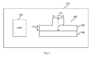
- FIG. 1 shows a block diagram of a Raman amplifier system with a semiconductor-on-insulator optical waveguide.
- FIG. 1 shows Raman amplifier system 100 which comprises an optical waveguide 102 and laser 104 .
- optical waveguide 102 is a semiconductor-on-insulator waveguide.
- rib-like waveguide layer 106 consists of crystalline silicon and is located on insulator 108 , such as silicon dioxide (SiO 2 ).
- the width 110 of waveguide layer 106 is between 0.5 ⁇ m to 10 ⁇ m, height 112 is between 1 ⁇ m and 10 ⁇ m, and height 114 is between 0.25 ⁇ m and 7 ⁇ m.
- the semiconductor material of waveguide layer 106 is isotopically purified for greater precision of the Raman amplification.
- Laser 104 serves as a source of pump light which is coupled into optical waveguide 102 for amplification of an optical signal which propagates through optical waveguide 102 .
- Raman amplifier system 100 It is a particular advantage of Raman amplifier system 100 that it can be implemented on a single integrated circuit chip with an interaction length of e.g. 0.25 cm to 1 cm.
- the length of optical waveguide 102 can even be shorter especially if isotopically purified semiconductor material is used for waveguide layer 106 .
Landscapes
- Physics & Mathematics (AREA)
- Electromagnetism (AREA)
- Engineering & Computer Science (AREA)
- Plasma & Fusion (AREA)
- Optics & Photonics (AREA)
- Optical Modulation, Optical Deflection, Nonlinear Optics, Optical Demodulation, Optical Logic Elements (AREA)
- Lasers (AREA)
- Amplifiers (AREA)
Applications Claiming Priority (2)
| Application Number | Priority Date | Filing Date | Title |
|---|---|---|---|
| EP03290956A EP1471612B1 (de) | 2003-04-17 | 2003-04-17 | Ramanverstärker |
| EP03290956.6 | 2003-04-17 |
Publications (2)
| Publication Number | Publication Date |
|---|---|
| US20040207908A1 US20040207908A1 (en) | 2004-10-21 |
| US7106500B2 true US7106500B2 (en) | 2006-09-12 |
Family
ID=32946954
Family Applications (1)
| Application Number | Title | Priority Date | Filing Date |
|---|---|---|---|
| US10/825,120 Expired - Lifetime US7106500B2 (en) | 2003-04-17 | 2004-04-16 | Raman amplifier system |
Country Status (4)
| Country | Link |
|---|---|
| US (1) | US7106500B2 (de) |
| EP (1) | EP1471612B1 (de) |
| AT (1) | ATE298143T1 (de) |
| DE (1) | DE60300859T2 (de) |
Families Citing this family (6)
| Publication number | Priority date | Publication date | Assignee | Title |
|---|---|---|---|---|
| WO2006014643A2 (en) * | 2004-07-20 | 2006-02-09 | The Trustees Of Columbia University In The City Of New York | Enhanced raman amplification and lasing in silicon-based photonic crystals |
| US7532656B2 (en) | 2005-02-16 | 2009-05-12 | The Trustees Of Columbia University In The City Of New York | All-silicon raman amplifiers and lasers based on micro ring resonators |
| WO2007027982A2 (en) * | 2005-08-31 | 2007-03-08 | The Trustees Of Columbia University In The City Of New York | Devices and methods for providing stimulated raman lasing |
| CN100375352C (zh) * | 2005-08-31 | 2008-03-12 | 中国科学院半导体研究所 | 硅基光子晶体微腔拉曼激光器结构 |
| US7411670B2 (en) | 2005-12-07 | 2008-08-12 | Ge Homeland Protection, Inc. | Collection probe for use in a Raman spectrometer system and methods of making and using the same |
| US10852621B1 (en) | 2019-07-03 | 2020-12-01 | Raytheon Company | System and method for generating multiple simultaneous, co-propagating wavelengths via nonlinear wavelength conversion |
Citations (5)
| Publication number | Priority date | Publication date | Assignee | Title |
|---|---|---|---|---|
| US4786140A (en) | 1987-10-30 | 1988-11-22 | Gte Laboratories Incorporated | Method of modulating large-power light beams using fiber raman amplification |
| US6483633B2 (en) | 2000-07-10 | 2002-11-19 | Sumitomo Electric Industries, Ltd. | Raman amplifier |
| GB2394553A (en) * | 2002-10-25 | 2004-04-28 | Qinetiq Ltd | Raman optical waveguide with refractive index modified by ion implantation and fabrication method |
| US6879604B2 (en) * | 1999-12-03 | 2005-04-12 | Qinetiq Limited | Waveguide laser devices |
| US6888667B2 (en) * | 2002-11-08 | 2005-05-03 | Intel Corporation | Method and apparatus for silicon-based optically-pumped amplification using stimulated scattering |
-
2003
- 2003-04-17 AT AT03290956T patent/ATE298143T1/de not_active IP Right Cessation
- 2003-04-17 DE DE60300859T patent/DE60300859T2/de not_active Expired - Lifetime
- 2003-04-17 EP EP03290956A patent/EP1471612B1/de not_active Expired - Lifetime
-
2004
- 2004-04-16 US US10/825,120 patent/US7106500B2/en not_active Expired - Lifetime
Patent Citations (5)
| Publication number | Priority date | Publication date | Assignee | Title |
|---|---|---|---|---|
| US4786140A (en) | 1987-10-30 | 1988-11-22 | Gte Laboratories Incorporated | Method of modulating large-power light beams using fiber raman amplification |
| US6879604B2 (en) * | 1999-12-03 | 2005-04-12 | Qinetiq Limited | Waveguide laser devices |
| US6483633B2 (en) | 2000-07-10 | 2002-11-19 | Sumitomo Electric Industries, Ltd. | Raman amplifier |
| GB2394553A (en) * | 2002-10-25 | 2004-04-28 | Qinetiq Ltd | Raman optical waveguide with refractive index modified by ion implantation and fabrication method |
| US6888667B2 (en) * | 2002-11-08 | 2005-05-03 | Intel Corporation | Method and apparatus for silicon-based optically-pumped amplification using stimulated scattering |
Non-Patent Citations (4)
| Title |
|---|
| K. Suto et al, "Raman amplification in GaP-AlxGal-xP waveguides for light frequency discrimination", IEE Proceedings: Optoelectronics, Institution of Electrical Engineers, Stevenage, GB, vol. 145, No. 2, Apr. 20, 1998, pp. 105-108, XP006011337. |
| K. Suto et al, "Semiconductor Raman Amplifier for Terahertz Bandwidth Optical Communication", Journal of Lightwave Technology, IEEE, New York, US, vol. 20, No. 4, Apr. 2002, pp. 705-711, XP001130032. |
| R. Claps et al, "Stimulated Raman scattering in silicon waveguides", Electronics Letters, IEE, Stevenage, GB, vol. 38, No. 22, Oct. 24 200, pp. 1352-1354, XP006019142. |
| T. Saito et al, "Gain of High-Intensity Pulse -Pumped Gap-Algap Waveguide Raman Amplifier", IEE Proceedings: Optoelectronics, Institution of Electrical Engineers, Stevenage, GB, vol. 146, No. 5, Oct. 1999, pp. 209-212, XP000928397. |
Also Published As
| Publication number | Publication date |
|---|---|
| US20040207908A1 (en) | 2004-10-21 |
| EP1471612A1 (de) | 2004-10-27 |
| ATE298143T1 (de) | 2005-07-15 |
| EP1471612B1 (de) | 2005-06-15 |
| DE60300859D1 (de) | 2005-07-21 |
| DE60300859T2 (de) | 2006-05-11 |
Similar Documents
| Publication | Publication Date | Title |
|---|---|---|
| US5287216A (en) | Fiber amplifier with multiple pumps | |
| JP2648435B2 (ja) | 2ビ−ム結合を用いた光エネルギ−の増幅方法および同方法を用いた光エネルギ−増幅装置 | |
| US6693740B2 (en) | Dispersion managed discrete Raman amplifiers | |
| US7489439B2 (en) | Semiconductor Raman ring amplifier | |
| US6363188B1 (en) | Mode expander with co-directional grating | |
| EP2930799B1 (de) | Angeordneter glasfaserverstärker unter verwendung von bandförmiger erbiumdotierter faser | |
| US7106500B2 (en) | Raman amplifier system | |
| US6721087B2 (en) | Optical amplifier with distributed evanescently-coupled pump | |
| US7046714B2 (en) | Method and apparatus for Raman ring resonator based laser/wavelength converter | |
| US6865018B2 (en) | Multistage optical amplifier having a fiber-based amplifier stage and a planar waveguide-based amplifier stage | |
| US20250329989A1 (en) | High-Power Optical Gain Waveguides | |
| JPWO2020071262A1 (ja) | 光増幅装置および光増幅方法 | |
| JP2667255B2 (ja) | 希土類元素添加ガラス導波路増幅器 | |
| CN100416946C (zh) | 具有多波长泵浦的光放大器 | |
| JP2693662B2 (ja) | 光増幅装置 | |
| JP4460298B2 (ja) | 多数の波長のポンピングを行う光増幅器 | |
| US20040076372A1 (en) | Optical amplification structure with an integrated optical system and amplification housing integrating one such structure | |
| JP2955780B2 (ja) | 光ファイバ増幅器 | |
| US7076130B2 (en) | Semiconductor optical device having asymmetric ridge waveguide and method of making same | |
| JP3042439B2 (ja) | 光ファイバ増幅器 | |
| US20050069251A1 (en) | Optical pump device with several output paths and use of same in an amplifier device | |
| WO2004068653A3 (en) | Traverse bragg resonance lasers and amplifiers and method of operating the same | |
| GB2386752A (en) | Optical amplifiers |
Legal Events
| Date | Code | Title | Description |
|---|---|---|---|
| AS | Assignment |
Owner name: ALCATEL, FRANCE Free format text: ASSIGNMENT OF ASSIGNORS INTEREST;ASSIGNORS:BASTIAN, GEORG;BOUROVA, EKATERINA;REEL/FRAME:015224/0096 Effective date: 20030520 |
|
| FEPP | Fee payment procedure |
Free format text: PAYOR NUMBER ASSIGNED (ORIGINAL EVENT CODE: ASPN); ENTITY STATUS OF PATENT OWNER: LARGE ENTITY |
|
| STCF | Information on status: patent grant |
Free format text: PATENTED CASE |
|
| FPAY | Fee payment |
Year of fee payment: 4 |
|
| FPAY | Fee payment |
Year of fee payment: 8 |
|
| AS | Assignment |
Owner name: OMEGA CREDIT OPPORTUNITIES MASTER FUND, LP, NEW YORK Free format text: SECURITY INTEREST;ASSIGNOR:WSOU INVESTMENTS, LLC;REEL/FRAME:043966/0574 Effective date: 20170822 Owner name: OMEGA CREDIT OPPORTUNITIES MASTER FUND, LP, NEW YO Free format text: SECURITY INTEREST;ASSIGNOR:WSOU INVESTMENTS, LLC;REEL/FRAME:043966/0574 Effective date: 20170822 |
|
| AS | Assignment |
Owner name: WSOU INVESTMENTS, LLC, CALIFORNIA Free format text: ASSIGNMENT OF ASSIGNORS INTEREST;ASSIGNOR:ALCATEL LUCENT;REEL/FRAME:044000/0053 Effective date: 20170722 |
|
| FEPP | Fee payment procedure |
Free format text: MAINTENANCE FEE REMINDER MAILED (ORIGINAL EVENT CODE: REM.) |
|
| FEPP | Fee payment procedure |
Free format text: 11.5 YR SURCHARGE- LATE PMT W/IN 6 MO, LARGE ENTITY (ORIGINAL EVENT CODE: M1556); ENTITY STATUS OF PATENT OWNER: LARGE ENTITY |
|
| MAFP | Maintenance fee payment |
Free format text: PAYMENT OF MAINTENANCE FEE, 12TH YEAR, LARGE ENTITY (ORIGINAL EVENT CODE: M1553); ENTITY STATUS OF PATENT OWNER: LARGE ENTITY Year of fee payment: 12 |
|
| AS | Assignment |
Owner name: BP FUNDING TRUST, SERIES SPL-VI, NEW YORK Free format text: SECURITY INTEREST;ASSIGNOR:WSOU INVESTMENTS, LLC;REEL/FRAME:049235/0068 Effective date: 20190516 |
|
| AS | Assignment |
Owner name: WSOU INVESTMENTS, LLC, CALIFORNIA Free format text: RELEASE BY SECURED PARTY;ASSIGNOR:OCO OPPORTUNITIES MASTER FUND, L.P. (F/K/A OMEGA CREDIT OPPORTUNITIES MASTER FUND LP;REEL/FRAME:049246/0405 Effective date: 20190516 |
|
| AS | Assignment |
Owner name: OT WSOU TERRIER HOLDINGS, LLC, CALIFORNIA Free format text: SECURITY INTEREST;ASSIGNOR:WSOU INVESTMENTS, LLC;REEL/FRAME:056990/0081 Effective date: 20210528 |
|
| AS | Assignment |
Owner name: WSOU INVESTMENTS, LLC, CALIFORNIA Free format text: RELEASE BY SECURED PARTY;ASSIGNOR:TERRIER SSC, LLC;REEL/FRAME:056526/0093 Effective date: 20210528 |