US7005643B2 - Infrared sensor - Google Patents

Infrared sensor Download PDF

Info

Publication number
US7005643B2
US7005643B2 US10/811,873 US81187304A US7005643B2 US 7005643 B2 US7005643 B2 US 7005643B2 US 81187304 A US81187304 A US 81187304A US 7005643 B2 US7005643 B2 US 7005643B2
Authority
US
United States
Prior art keywords
membrane
infrared sensor
adhesive
substrate
infrared
Prior art date
Legal status (The legal status is an assumption and is not a legal conclusion. Google has not performed a legal analysis and makes no representation as to the accuracy of the status listed.)
Expired - Fee Related
Application number
US10/811,873
Other versions
US20040188618A1 (en
Inventor
Kazuaki Hamamoto
Current Assignee (The listed assignees may be inaccurate. Google has not performed a legal analysis and makes no representation or warranty as to the accuracy of the list.)
Denso Corp
Original Assignee
Denso Corp
Priority date (The priority date is an assumption and is not a legal conclusion. Google has not performed a legal analysis and makes no representation as to the accuracy of the date listed.)
Filing date
Publication date
Application filed by Denso Corp filed Critical Denso Corp
Assigned to DENSO CORPORATION reassignment DENSO CORPORATION ASSIGNMENT OF ASSIGNORS INTEREST (SEE DOCUMENT FOR DETAILS). Assignors: HAMAMOTO, KAZUAKI
Publication of US20040188618A1 publication Critical patent/US20040188618A1/en
Application granted granted Critical
Publication of US7005643B2 publication Critical patent/US7005643B2/en
Anticipated expiration legal-status Critical
Expired - Fee Related legal-status Critical Current

Links

Images

Classifications

    • BPERFORMING OPERATIONS; TRANSPORTING
    • B81MICROSTRUCTURAL TECHNOLOGY
    • B81CPROCESSES OR APPARATUS SPECIALLY ADAPTED FOR THE MANUFACTURE OR TREATMENT OF MICROSTRUCTURAL DEVICES OR SYSTEMS
    • B81C3/00Assembling of devices or systems from individually processed components
    • B81C3/001Bonding of two components
    • GPHYSICS
    • G01MEASURING; TESTING
    • G01JMEASUREMENT OF INTENSITY, VELOCITY, SPECTRAL CONTENT, POLARISATION, PHASE OR PULSE CHARACTERISTICS OF INFRARED, VISIBLE OR ULTRAVIOLET LIGHT; COLORIMETRY; RADIATION PYROMETRY
    • G01J5/00Radiation pyrometry, e.g. infrared or optical thermometry
    • G01J5/10Radiation pyrometry, e.g. infrared or optical thermometry using electric radiation detectors

Definitions

  • the present invention relates to an infrared sensor structured as a membrane and provided with an infrared detector generating an electric signal based on changes in temperature occurring at the time of receiving infrared rays, more particularly relates to an infrared sensor mounted by bonding with a mounting surface constituted by a sensor support using an adhesive.
  • An object of the present invention is to provide an infrared sensor formed as a membrane on a substrate and detecting infrared rays by an infrared detector on that membrane, wherein even if an adhesive used for mounting the infrared sensor on a mounting surface creeps up to the membrane, it is possible to prevent a drop in the sensor sensitivity.
  • an infrared sensor mounted on a mounting surface by an adhesive having a heat conductivity of not more than seven times the heat conductivity of a fluid present in an inner cavity below the membrane.
  • FIG. 1( a ) is a perspective view of an infrared sensor according to a first embodiment of the present invention having a membrane structure, while FIG. 1( b ) is a cross-sectional view along the line A′–A of the infrared sensor shown in FIG. 1( a );
  • FIG. 2 is a view of the state of the adhesive creeping up and reaching the membrane at the time of mounting
  • FIG. 3( a ) is a perspective view of an infrared sensor according to a second embodiment of the present invention having a membrane structure
  • FIG. 3( b ) is a cross-sectional view along the line A′–A of the infrared sensor shown in FIG. 3( a )
  • FIG. 3( c ) is a view of thermocouples provided on the substrate;
  • FIG. 4 is a view of the temperature distribution of the sensor surface in the infrared sensor 10 according to the second embodiment of the present invention.
  • FIG. 5( a ) is a perspective view of an infrared sensor according to the related art having a membrane structure
  • FIG. 5( b ) is a cross-sectional view along the line A′–A of the infrared sensor shown in FIG. 5( a )
  • FIG. 5( c ) is a view of thermocouples provided on the substrate;
  • FIGS. 6( a ) to 6 ( c ) are views of the states of an adhesive creeping up along the inside walls of an inner cavity of a substrate under a membrane;
  • FIG. 7 is a view of an example of a semiconductor sensor of the related art.
  • FIG. 5( a ) is a perspective view of an infrared sensor of the related art having a membrane structure
  • FIG. 5( b ) is a cross-sectional view along the line A′–A of the infrared sensor shown in FIG. 5( a ).
  • the infrared sensor 10 of the related art is obtained by etching the back surface of a silicon chip substrate 12 and forming a membrane 14 at the thin part of the substrate.
  • the substrate 12 having the membrane 14 is provided on its top surface with plurality of thermocouples 20 having hot contact parts 22 on the membrane 14 and cold contact parts 25 on the thick part outside of the membrane 14 .
  • the hot contact parts of the thermocouples 20 are covered by an infrared ray absorption film 26 .
  • the infrared ray absorption film 26 is comprised of a polyester resin containing carbon and is cured by heat. This absorbs infrared rays and enables the temperature of the hot contact parts to be efficiently raised.
  • the substrate 12 is bonded to the mounting surface constituted by the sensor support 40 by an adhesive 30 for mounting.
  • FIG. 5( c ) shows thermocouples 20 provided on the top surface of the substrate 12 .
  • the infrared ray absorption film 26 absorbs the infrared rays and rises in temperature.
  • the hot contact parts 22 provided on the membrane 14 rise in temperature since the path for conduction of the heat conducted from the infrared ray absorption film 26 is small, while the cold contact parts 24 provided on the thick part at the outside of the membrane do not rise in temperature as the substrate 12 serves as a heat sink.
  • a temperature difference is caused between the hot contact parts 22 and the cold contact parts 24 and an electromotive force is generated by the Seebeck effect.
  • a plurality of the thermocouples 20 are arranged in series as shown in the figure. The sum Vout of the electromotive forces of the thermocouples becomes the output of the sensor.
  • the adhesive 30 used in the infrared sensor 10 of the related art was a silver paste having a heat conductivity of about 5 W/mK. This was because an adhesive with a high heat conductivity was preferred so as to facilitate the escape of heat of the thick part of the substrate to the sensor support 40 , so that increase the temperature difference between the hot contact parts 22 and cold contact parts 24 is increased and the sensitivity of the infrared sensor 10 is improved. Note that, as an infrared sensor having such a membrane structure, there is the semiconductor chip disclosed in Japanese Unexamined Patent Publication (Kokai) No. 7-58134 (paragraphs [0016] to [0020]).
  • FIG. 6( a ) shows the state of the adhesive 30 reaching the back surface of the membrane 14 .
  • the inner cavity 18 below the membrane 14 contains a low heat conductivity gas with a low heat conductivity of not more than 0.025 W/mK. Due to this, the heat capacity of the hot contact parts 22 is reduced. Accordingly, as shown in FIG. 6( b ), it is possible to prevent a drop in the temperature of the membrane 14 and hold the temperature of the hot contact parts 22 as they are when the adhesive does not creep up along the inside walls 19 .
  • the present invention provides an infrared sensor wherein even if an adhesive used for mounting the infrared sensor on a mounting creeps up to the membrane, it is possible to prevent a drop in the sensor sensitivity.
  • the infrared sensor according to the present invention is mounted on a mounting surface by an adhesive having a heat conductivity of not more than seven times the heat conductivity of a fluid present in the inner cavity surrounded by the bottom surface of the substrate below the membrane and the mounting surface.
  • FIG. 1( a ) is a perspective view of an infrared sensor according to a first embodiment of the present invention having a membrane structure
  • FIG. 1( b ) is a cross-sectional view along the line A′–A shown in FIG. 1( a ).
  • the infrared sensor 10 is obtained by etching the back surface of a silicon chip substrate 12 and forming a membrane 14 .
  • the top surface of the substrate 12 having the membrane 14 is provided with an infrared detector 28 .
  • the infrared sensor 10 is bonded at its bottom surface 16 with a sensor support 40 by an adhesive 30 for mounting.
  • the inner cavity 18 below the membrane 14 contains a low heat conductivity gas having a heat conductivity of 0 W/mK to 0.025 W/mK and reduces the heat capacity of the infrared detector 28 . Therefore, as shown in FIG. 1( b ), when the adhesive does not creep up along the inside walls 19 , it is possible to prevent a drop in temperature of the membrane 14 and maintain the temperature of the infrared detector 28 as it is.
  • the infrared sensor 10 uses an adhesive with a low heat conductivity instead of the adhesive with a high heat conductivity such as the silver paste used in the related art (heat conductivity of 5 W/mK) as the adhesive used for mounting to the sensor support 40 .
  • the adhesive with a low heat conductivity and able to be used for bonding a sensor such as the infrared sensor 10 of the present invention a silicone-based adhesive having a heat conductivity of 0.16 W/mK or so can be suitably used.
  • FIG. 2 is a view of the state where the adhesive has creeped up along the inner walls 19 of the substrate 12 and reached the membrane 14 . Even if the adhesive 30 creeps up and reaches the membrane 14 as shown in FIG. 2 , since the heat conductivity of the adhesive 30 used for the infrared sensor 10 according to the present invention is low as explained above, the heat transfer path by the adhesive 30 reaching the membrane 14 is small and therefore the heat capacity of the infrared detector 28 can be kept small.
  • FIG. 3( a ) is a perspective view of an infrared sensor according to a second embodiment of the present invention having a membrane structure
  • FIG. 3( b ) is a cross-sectional view along the line A′–A of FIG. 3( a ).
  • the infrared sensor 10 is provided with a plurality of thermocouples 20 having hot contact parts 22 on the membrane 14 and cold contact parts 24 on the thick part at the outside of the membrane 14 .
  • the hot contact parts of the thermocouples 20 are covered by the infrared ray absorption film 26 .
  • FIG. 3( c ) shows the thermocouples 20 provided on the top surface of the substrate 12 .
  • the infrared ray absorption film 26 absorbs the infrared rays and rises in temperature.
  • the hot contact parts 22 provided on the membrane 14 rise in temperature since the path for conduction of the heat conducted from the infrared ray absorption film 26 is small, while the cold contact parts 24 provided on the thick part at the outside of the membrane do not rise in temperature as the substrate 12 serves as a heat sink.
  • a temperature difference is caused between the hot contact parts 22 and the cold contact parts 24 , and a sensor output Vout corresponding to this temperature difference is output.
  • FIG. 4 shows the temperature distribution of the sensor surface in the infrared sensor 10 according to a second embodiment of the present invention.
  • the illustrated graph shows the results of analysis of the temperature distribution of the surface of the infrared sensor 10 in the case of making the heat conductivity of the fluid present in the hollow part 18 not more than 0.025 W/mK, making the heat conductivity of the adhesive 30 not more than 0.18 W/mK or not more than about seven times the heat conductivity of the low heat conductivity gas, and in the presence and absence of creep of the adhesive 30 .

Abstract

An infrared sensor formed as a membrane on a substrate and detecting infrared rays by an infrared detector on that membrane, wherein even if an adhesive used for mounting the infrared sensor on a mounting surface creeps up to the membrane, it is made possible to prevent a drop in the sensor sensitivity by mounting the infrared sensor on a mounting surface by an adhesive having a heat conductivity of not more than seven times the heat conductivity of a fluid present in the inner cavity below the membrane.

Description

BACKGROUND OF THE INVENTION
1. Field of the Invention
The present invention relates to an infrared sensor structured as a membrane and provided with an infrared detector generating an electric signal based on changes in temperature occurring at the time of receiving infrared rays, more particularly relates to an infrared sensor mounted by bonding with a mounting surface constituted by a sensor support using an adhesive.
2. Description of the Related Art
As will be explained in detail later with reference to the drawings, when mounting an infrared sensor on a sensor support using an adhesive, the excess adhesive squeezed out from the bottom of the substrate of the infrared sensor creeps up along the inside walls of the inner cavity of the substrate below the membrane. If reaching the membrane, the temperature difference between the hot contacts and cold contacts of the thermocouples will become small and a drop in sensor sensitivity will be caused.
In the semiconductor sensor disclosed in Japanese Unexamined Patent Publication (Kokai) No. 7-58134 as related art, to prevent this creep of the adhesive, as shown in the later drawings, an adhesive constituted by a die bonding paste is provided locally rather than over the entire bottom surface of the substrate. With this mounting method, however, it is necessary to control the coating positions and amounts of coating of the adhesive in the mounting step of the infrared sensor. This is troublesome.
SUMMARY OF THE INVENTION
An object of the present invention is to provide an infrared sensor formed as a membrane on a substrate and detecting infrared rays by an infrared detector on that membrane, wherein even if an adhesive used for mounting the infrared sensor on a mounting surface creeps up to the membrane, it is possible to prevent a drop in the sensor sensitivity.
To attain the above object, there is provided an infrared sensor mounted on a mounting surface by an adhesive having a heat conductivity of not more than seven times the heat conductivity of a fluid present in an inner cavity below the membrane.
BRIEF DESCRIPTION OF THE DRAWINGS
These and other objects and features of the present invention will become clearer from the following description of the preferred embodiments given with reference to the attached drawings, wherein:
FIG. 1( a) is a perspective view of an infrared sensor according to a first embodiment of the present invention having a membrane structure, while FIG. 1( b) is a cross-sectional view along the line A′–A of the infrared sensor shown in FIG. 1( a);
FIG. 2 is a view of the state of the adhesive creeping up and reaching the membrane at the time of mounting;
FIG. 3( a) is a perspective view of an infrared sensor according to a second embodiment of the present invention having a membrane structure, FIG. 3( b) is a cross-sectional view along the line A′–A of the infrared sensor shown in FIG. 3( a), and FIG. 3( c) is a view of thermocouples provided on the substrate;
FIG. 4 is a view of the temperature distribution of the sensor surface in the infrared sensor 10 according to the second embodiment of the present invention;
FIG. 5( a) is a perspective view of an infrared sensor according to the related art having a membrane structure, FIG. 5( b) is a cross-sectional view along the line A′–A of the infrared sensor shown in FIG. 5( a), and FIG. 5( c) is a view of thermocouples provided on the substrate;
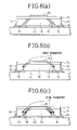
FIGS. 6( a) to 6(c) are views of the states of an adhesive creeping up along the inside walls of an inner cavity of a substrate under a membrane; and
FIG. 7 is a view of an example of a semiconductor sensor of the related art.
DESCRIPTION OF THE PREFERRED EMBODIMENTS
Before describing the embodiments of the present invention, the related art and the disadvantages therein will be described with reference to the related figures.
In general, as an infrared sensor having a membrane structure, a thermopile type infrared sensor is well known. FIG. 5( a) is a perspective view of an infrared sensor of the related art having a membrane structure, while FIG. 5( b) is a cross-sectional view along the line A′–A of the infrared sensor shown in FIG. 5( a).
The infrared sensor 10 of the related art is obtained by etching the back surface of a silicon chip substrate 12 and forming a membrane 14 at the thin part of the substrate. The substrate 12 having the membrane 14 is provided on its top surface with plurality of thermocouples 20 having hot contact parts 22 on the membrane 14 and cold contact parts 25 on the thick part outside of the membrane 14. The hot contact parts of the thermocouples 20 are covered by an infrared ray absorption film 26. The infrared ray absorption film 26 is comprised of a polyester resin containing carbon and is cured by heat. This absorbs infrared rays and enables the temperature of the hot contact parts to be efficiently raised. The substrate 12 is bonded to the mounting surface constituted by the sensor support 40 by an adhesive 30 for mounting.
FIG. 5( c) shows thermocouples 20 provided on the top surface of the substrate 12. When infrared rays from the human body etc. strike the substrate, the infrared ray absorption film 26 absorbs the infrared rays and rises in temperature. As a result, the hot contact parts 22 provided on the membrane 14 rise in temperature since the path for conduction of the heat conducted from the infrared ray absorption film 26 is small, while the cold contact parts 24 provided on the thick part at the outside of the membrane do not rise in temperature as the substrate 12 serves as a heat sink. As a result, a temperature difference is caused between the hot contact parts 22 and the cold contact parts 24 and an electromotive force is generated by the Seebeck effect. A plurality of the thermocouples 20 are arranged in series as shown in the figure. The sum Vout of the electromotive forces of the thermocouples becomes the output of the sensor.
The adhesive 30 used in the infrared sensor 10 of the related art was a silver paste having a heat conductivity of about 5 W/mK. This was because an adhesive with a high heat conductivity was preferred so as to facilitate the escape of heat of the thick part of the substrate to the sensor support 40, so that increase the temperature difference between the hot contact parts 22 and cold contact parts 24 is increased and the sensitivity of the infrared sensor 10 is improved. Note that, as an infrared sensor having such a membrane structure, there is the semiconductor chip disclosed in Japanese Unexamined Patent Publication (Kokai) No. 7-58134 (paragraphs [0016] to [0020]).
As explained above, when using an adhesive for mounting the infrared sensor 10 on the sensor support 40, the excess adhesive 30 squeezed out from the bottom surface 16 of the substrate 12 at the time of mounting creeps up along the inside walls 19 of the inner cavity 18 of the substrate 12 under the membrane 14 and is liable to reach the back surface of the membrane 14. FIG. 6( a) shows the state of the adhesive 30 reaching the back surface of the membrane 14.
The inner cavity 18 below the membrane 14 contains a low heat conductivity gas with a low heat conductivity of not more than 0.025 W/mK. Due to this, the heat capacity of the hot contact parts 22 is reduced. Accordingly, as shown in FIG. 6( b), it is possible to prevent a drop in the temperature of the membrane 14 and hold the temperature of the hot contact parts 22 as they are when the adhesive does not creep up along the inside walls 19.
However, when the adhesive 30 creeps up along the inside walls 19 and reaches the membrane 14 as shown in FIG. 6( c), the heat capacity of the hot contact parts 22 ends up becoming larger due to the formation of a heat transfer path by the adhesive 30 with the heat conductivity higher than the fluid in the inner cavity 18. As a result, the temperature difference between the hot contacts and the cold contacts becomes smaller and a drop in the sensor sensitivity is caused.
In the semiconductor sensor disclosed in Japanese Unexamined Patent Publication (Kokai) No. 7-58134, as explained above, as shown in FIG. 7, an adhesive 30 constituted by a die bonding paste was provided locally rather than over the entire bottom surface of the substrate 12 so as to prevent the above creeping up of the adhesive 30. According to this method, however, to prevent the adhesive 30 from creeping up, it was necessary to control the coating positions and amounts of coating of the adhesive 30 in the mounting step of the infrared sensor 10. This was troublesome as mentioned before.
In view of this problem, the present invention provides an infrared sensor wherein even if an adhesive used for mounting the infrared sensor on a mounting creeps up to the membrane, it is possible to prevent a drop in the sensor sensitivity.
For this purpose, the infrared sensor according to the present invention is mounted on a mounting surface by an adhesive having a heat conductivity of not more than seven times the heat conductivity of a fluid present in the inner cavity surrounded by the bottom surface of the substrate below the membrane and the mounting surface.
By mounting with a low heat conductivity adhesive in this way, even if creep of the adhesive occurs at the time of mounting and the adhesive reaches the membrane, the conduction of heat due to the heat transfer path formed by the creeping adhesive can be suppressed and the heat capacity of the infrared detector can be kept small. Due to this, it becomes possible to prevent a drop in sensor sensitivity of the infrared sensor.
Next, an infrared sensor according to a first embodiment of the present invention will be explained with reference to the attached drawings. FIG. 1( a) is a perspective view of an infrared sensor according to a first embodiment of the present invention having a membrane structure, while FIG. 1( b) is a cross-sectional view along the line A′–A shown in FIG. 1( a).
The infrared sensor 10 according to the present invention is obtained by etching the back surface of a silicon chip substrate 12 and forming a membrane 14. The top surface of the substrate 12 having the membrane 14 is provided with an infrared detector 28. Here, the infrared sensor 10 is bonded at its bottom surface 16 with a sensor support 40 by an adhesive 30 for mounting.
The inner cavity 18 below the membrane 14 contains a low heat conductivity gas having a heat conductivity of 0 W/mK to 0.025 W/mK and reduces the heat capacity of the infrared detector 28. Therefore, as shown in FIG. 1( b), when the adhesive does not creep up along the inside walls 19, it is possible to prevent a drop in temperature of the membrane 14 and maintain the temperature of the infrared detector 28 as it is.
The infrared sensor 10 according to the present invention uses an adhesive with a low heat conductivity instead of the adhesive with a high heat conductivity such as the silver paste used in the related art (heat conductivity of 5 W/mK) as the adhesive used for mounting to the sensor support 40. As the adhesive with a low heat conductivity and able to be used for bonding a sensor such as the infrared sensor 10 of the present invention, a silicone-based adhesive having a heat conductivity of 0.16 W/mK or so can be suitably used.
FIG. 2 is a view of the state where the adhesive has creeped up along the inner walls 19 of the substrate 12 and reached the membrane 14. Even if the adhesive 30 creeps up and reaches the membrane 14 as shown in FIG. 2, since the heat conductivity of the adhesive 30 used for the infrared sensor 10 according to the present invention is low as explained above, the heat transfer path by the adhesive 30 reaching the membrane 14 is small and therefore the heat capacity of the infrared detector 28 can be kept small.
In this way, by using an adhesive with a low heat conductivity as the adhesive 30 used for mounting to the sensor support 40, even if the adhesive 30 squeezed out from the bottom surface 16 of the substrate 12 at the time of mounting creeps up along the inner walls 19 of the substrate 12 and reaches the membrane 14, the heat capacity of the infrared detector 28 can be kept small and therefore the drop in sensor sensitivity can be prevented.
FIG. 3( a) is a perspective view of an infrared sensor according to a second embodiment of the present invention having a membrane structure, while FIG. 3( b) is a cross-sectional view along the line A′–A of FIG. 3( a).
The infrared sensor 10 according to the second embodiment is provided with a plurality of thermocouples 20 having hot contact parts 22 on the membrane 14 and cold contact parts 24 on the thick part at the outside of the membrane 14. The hot contact parts of the thermocouples 20 are covered by the infrared ray absorption film 26.
FIG. 3( c) shows the thermocouples 20 provided on the top surface of the substrate 12. When infrared rays strike the substrate, the infrared ray absorption film 26 absorbs the infrared rays and rises in temperature. As a result, the hot contact parts 22 provided on the membrane 14 rise in temperature since the path for conduction of the heat conducted from the infrared ray absorption film 26 is small, while the cold contact parts 24 provided on the thick part at the outside of the membrane do not rise in temperature as the substrate 12 serves as a heat sink. As a result, a temperature difference is caused between the hot contact parts 22 and the cold contact parts 24, and a sensor output Vout corresponding to this temperature difference is output.
When using a low heat conductivity adhesive 30 for mounting the infrared sensor to the sensor support 40, there is the problem that the heat of the thick part of the substrate 12 forming the heat sink of the cold contact parts 24 becomes difficult to relieve to the sensor support 40. However, the function as a heat sink for the cold contact parts 24 can be performed by just the substrate 12, so even if using a low heat conductivity adhesive 30, there is not an effect enough to cause problems in the sensor characteristics.
FIG. 4 shows the temperature distribution of the sensor surface in the infrared sensor 10 according to a second embodiment of the present invention. The illustrated graph shows the results of analysis of the temperature distribution of the surface of the infrared sensor 10 in the case of making the heat conductivity of the fluid present in the hollow part 18 not more than 0.025 W/mK, making the heat conductivity of the adhesive 30 not more than 0.18 W/mK or not more than about seven times the heat conductivity of the low heat conductivity gas, and in the presence and absence of creep of the adhesive 30.
AS shown in FIG. 4, it is learned that regardless of creep of the adhesive, the temperature distribution of the surface becomes substantially the same. Due to this, it is learned that if making the heat conductivity of the adhesive 30 not more than 0.18 W/mK or not more than about seven times the heat conductivity of the low heat conductivity gas present in the cavity 18 of the sensor 10, it is possible to suppress any effects of the creep of adhesive 30 on the sensor sensitivity of the infrared sensor 10.
While the invention has been described with reference to specific embodiments chosen for purpose of illustration, it should be apparent that numerous modifications could be made thereto by those skilled in the art without departing from the basic concept and scope of the invention.

Claims (10)

1. An infrared senor provided with a substrate having a thick part and a thin part, a membrane constituting the thin part of said substrate, and an infrared detector provided on a top surface of said substrate having said membrane, wherein:
a bottom surface of the thick part of said substrate and a mounting surface for mounting said infrared sensor are bonded by an adhesive for mounting, and
said adhesive consists of a material having a heat conductivity not exceeding seven times the heat conductivity of a fluid present in an inner cavity surrounded by the bottom surface of said substrate and said mounting surface.
2. An infrared sensor as set forth in claim 1, wherein
said bottom surface of said substrate and said mounting surface are bonded by an adhesive having a heat conductivity of not more than 0.18 W/mK for mounting.
3. An infrared sensor as set forth in claim 1, wherein said adhesive is a silicone-based adhesive.
4. An infrared sensor as set forth in claim 2, wherein said adhesive is a silicone-based adhesive.
5. An infrared sensor as act forth in claim 1, wherein said infrared detector is provided with:
a thermocouple providing a hot contact part on said membrane and providing a cold contact part outside of said membrane on said substrate and
an infrared ray absorption film formed on said membrane so as to cover said hot contact part.
6. An infrared sensor as set forth in claim 2, wherein said infrared detector is provided with:
a thermocouple providing a hot contact part on said membrane and providing a cold contact part outside of said membrane on said substrate and
an infrared ray absorption film formed on said membrane so as to cover said hot contact part.
7. An infrared sensor as set forth in claim 1, wherein said fluid is a low conductivity gas.
8. An infrared sensor as set forth in claim 2, wherein said fluid is a low conductivity gas.
9. An infrared sensor as set forth in claim 1, wherein a heat conductivity of said fluid is not more than 0.025 W/mK.
10. An infrared sensor as set forth in claim 2, wherein a heat conductivity of said fluid is not more than 0.025 W/mK.
US10/811,873 2003-03-31 2004-03-30 Infrared sensor Expired - Fee Related US7005643B2 (en)

Applications Claiming Priority (2)

Application Number Priority Date Filing Date Title
JP2003-96380 2003-03-31
JP2003096380A JP2004301744A (en) 2003-03-31 2003-03-31 Infrared sensor

Publications (2)

Publication Number Publication Date
US20040188618A1 US20040188618A1 (en) 2004-09-30
US7005643B2 true US7005643B2 (en) 2006-02-28

Family

ID=32985487

Family Applications (1)

Application Number Title Priority Date Filing Date
US10/811,873 Expired - Fee Related US7005643B2 (en) 2003-03-31 2004-03-30 Infrared sensor

Country Status (2)

Country Link
US (1) US7005643B2 (en)
JP (1) JP2004301744A (en)

Cited By (3)

* Cited by examiner, † Cited by third party
Publication number Priority date Publication date Assignee Title
US20050012588A1 (en) * 2003-07-16 2005-01-20 Sultan Michel F. Temperature sensor apparatus and method
US20070297485A1 (en) * 2004-06-09 2007-12-27 Perkinelmer Optoelectronics Gmbh & Co. Kg Sensor Element
US20180335347A1 (en) * 2015-11-27 2018-11-22 Heimann Sensor Gmbh Thermal infrared sensor array in wafer-level package

Families Citing this family (3)

* Cited by examiner, † Cited by third party
Publication number Priority date Publication date Assignee Title
EP1976034A3 (en) * 2007-03-29 2011-11-09 Stichting IMEC Nederland Method for manufacturing a thermopile, the thermopile thus obtrained and a thermoelectric generator comprising such thermopiles
CN103148947B (en) * 2013-03-21 2016-03-16 江苏物联网研究发展中心 Improve the wafer level packaging structure of thermopile IR detector responsiveness
CN107478343B (en) * 2016-06-07 2018-09-11 上海新微技术研发中心有限公司 Radiometer and method for manufacturing the same

Citations (8)

* Cited by examiner, † Cited by third party
Publication number Priority date Publication date Assignee Title
US3596096A (en) * 1970-03-13 1971-07-27 Us Air Force Dual temperature apparatus for testing infrared radiation detectors
JPH03196583A (en) * 1989-03-24 1991-08-28 Nippon Steel Corp Vertical type silicon thermopile and manufacture thereof
US5056929A (en) * 1990-01-30 1991-10-15 Citizen Watch Co., Ltd. Temperature compensation type infrared sensor
US5099120A (en) * 1989-06-20 1992-03-24 U.S. Philips Corporation Thermal-radiation detectors, detection systems and their manufacture
JPH06194229A (en) 1992-10-27 1994-07-15 Matsushita Electric Works Ltd Infrared ray sensor
JPH0758134A (en) 1993-06-30 1995-03-03 Matsushita Electric Works Ltd Semiconductor device and device and method for mounting same
JPH0888411A (en) * 1994-09-16 1996-04-02 Nissan Motor Co Ltd Infrared sensor
JPH08122161A (en) 1994-10-24 1996-05-17 Ricoh Seiki Co Ltd Heat-dependence detection device

Patent Citations (8)

* Cited by examiner, † Cited by third party
Publication number Priority date Publication date Assignee Title
US3596096A (en) * 1970-03-13 1971-07-27 Us Air Force Dual temperature apparatus for testing infrared radiation detectors
JPH03196583A (en) * 1989-03-24 1991-08-28 Nippon Steel Corp Vertical type silicon thermopile and manufacture thereof
US5099120A (en) * 1989-06-20 1992-03-24 U.S. Philips Corporation Thermal-radiation detectors, detection systems and their manufacture
US5056929A (en) * 1990-01-30 1991-10-15 Citizen Watch Co., Ltd. Temperature compensation type infrared sensor
JPH06194229A (en) 1992-10-27 1994-07-15 Matsushita Electric Works Ltd Infrared ray sensor
JPH0758134A (en) 1993-06-30 1995-03-03 Matsushita Electric Works Ltd Semiconductor device and device and method for mounting same
JPH0888411A (en) * 1994-09-16 1996-04-02 Nissan Motor Co Ltd Infrared sensor
JPH08122161A (en) 1994-10-24 1996-05-17 Ricoh Seiki Co Ltd Heat-dependence detection device

Cited By (6)

* Cited by examiner, † Cited by third party
Publication number Priority date Publication date Assignee Title
US20050012588A1 (en) * 2003-07-16 2005-01-20 Sultan Michel F. Temperature sensor apparatus and method
US7131766B2 (en) * 2003-07-16 2006-11-07 Delphi Technologies, Inc. Temperature sensor apparatus and method
US20070297485A1 (en) * 2004-06-09 2007-12-27 Perkinelmer Optoelectronics Gmbh & Co. Kg Sensor Element
US8215831B2 (en) * 2004-06-09 2012-07-10 Excelitas Technologies Gmbh & Co. Kg Sensor element
US20180335347A1 (en) * 2015-11-27 2018-11-22 Heimann Sensor Gmbh Thermal infrared sensor array in wafer-level package
US10788370B2 (en) * 2015-11-27 2020-09-29 Heimann Sensor Gmbh Thermal infrared sensor array in wafer-level package

Also Published As

Publication number Publication date
US20040188618A1 (en) 2004-09-30
JP2004301744A (en) 2004-10-28

Similar Documents

Publication Publication Date Title
EP0734589B1 (en) Integrated silicon vacuum micropackage for infrared devices
US7309865B2 (en) Electronic device having infrared sensing elements
US10060803B2 (en) MEMS internal temperature sensor having thin film thermopile
EP2310805B1 (en) Sensing environmental parameter through stress induced in ic
US20060169902A1 (en) Infrared sensor
WO2002075262A1 (en) Infrared detection element and method for fabricating the same and equipment for measuring temperature
JPS6129648B2 (en)
CN102150021A (en) Planar thermopile infrared microsensor
US7005643B2 (en) Infrared sensor
KR100591390B1 (en) Sensor having membrane and method for manufacturing the same
JP7394060B2 (en) infrared device
JP2010071816A (en) Electronic device
JP2007501404A (en) Infrared sensor utilizing optimized surface
US20040264009A1 (en) Temperature controlled optoelectronic device
JP5043556B2 (en) Hydrogen gas sensor
JPH06137943A (en) Thermal infrared sensor
JPH02205730A (en) Infrared-ray sensor
JP2005147768A (en) Infrared detector
WO2022038681A1 (en) Infrared sensor device
JP2006047086A (en) Infrared sensor
JP2005227180A (en) Infrared detector
JP4844198B2 (en) Semiconductor element, sensor device, and method for manufacturing semiconductor element
JP2955867B2 (en) Infrared sensor and method of manufacturing the same
JPH046424A (en) Infrared sensor
JPH0539467Y2 (en)

Legal Events

Date Code Title Description
AS Assignment

Owner name: DENSO CORPORATION, JAPAN

Free format text: ASSIGNMENT OF ASSIGNORS INTEREST;ASSIGNOR:HAMAMOTO, KAZUAKI;REEL/FRAME:015160/0641

Effective date: 20040319

FPAY Fee payment

Year of fee payment: 4

FEPP Fee payment procedure

Free format text: PAYOR NUMBER ASSIGNED (ORIGINAL EVENT CODE: ASPN); ENTITY STATUS OF PATENT OWNER: LARGE ENTITY

FPAY Fee payment

Year of fee payment: 8

FEPP Fee payment procedure

Free format text: MAINTENANCE FEE REMINDER MAILED (ORIGINAL EVENT CODE: REM.)

LAPS Lapse for failure to pay maintenance fees

Free format text: PATENT EXPIRED FOR FAILURE TO PAY MAINTENANCE FEES (ORIGINAL EVENT CODE: EXP.)

STCH Information on status: patent discontinuation

Free format text: PATENT EXPIRED DUE TO NONPAYMENT OF MAINTENANCE FEES UNDER 37 CFR 1.362

FP Lapsed due to failure to pay maintenance fee

Effective date: 20180228