US6982187B2 - Methods of making shallow trench-type pixels for CMOS image sensors - Google Patents
Methods of making shallow trench-type pixels for CMOS image sensors Download PDFInfo
- Publication number
- US6982187B2 US6982187B2 US10/606,693 US60669303A US6982187B2 US 6982187 B2 US6982187 B2 US 6982187B2 US 60669303 A US60669303 A US 60669303A US 6982187 B2 US6982187 B2 US 6982187B2
- Authority
- US
- United States
- Prior art keywords
- shallow trench
- pixel
- doped
- forming
- photoresist layer
- Prior art date
- Legal status (The legal status is an assumption and is not a legal conclusion. Google has not performed a legal analysis and makes no representation as to the accuracy of the status listed.)
- Expired - Fee Related
Links
Images


Classifications
-
- H—ELECTRICITY
- H10—SEMICONDUCTOR DEVICES; ELECTRIC SOLID-STATE DEVICES NOT OTHERWISE PROVIDED FOR
- H10F—INORGANIC SEMICONDUCTOR DEVICES SENSITIVE TO INFRARED RADIATION, LIGHT, ELECTROMAGNETIC RADIATION OF SHORTER WAVELENGTH OR CORPUSCULAR RADIATION
- H10F39/00—Integrated devices, or assemblies of multiple devices, comprising at least one element covered by group H10F30/00, e.g. radiation detectors comprising photodiode arrays
- H10F39/10—Integrated devices
- H10F39/12—Image sensors
-
- H—ELECTRICITY
- H10—SEMICONDUCTOR DEVICES; ELECTRIC SOLID-STATE DEVICES NOT OTHERWISE PROVIDED FOR
- H10F—INORGANIC SEMICONDUCTOR DEVICES SENSITIVE TO INFRARED RADIATION, LIGHT, ELECTROMAGNETIC RADIATION OF SHORTER WAVELENGTH OR CORPUSCULAR RADIATION
- H10F39/00—Integrated devices, or assemblies of multiple devices, comprising at least one element covered by group H10F30/00, e.g. radiation detectors comprising photodiode arrays
- H10F39/011—Manufacture or treatment of image sensors covered by group H10F39/12
- H10F39/014—Manufacture or treatment of image sensors covered by group H10F39/12 of CMOS image sensors
Definitions
- CMOS complimentary metal-oxide semiconductors
- a pixel detects an image by accepting light rays in an area on which a photodiode is formed.
- a photodiode is a device that produces electrical signals by generating electron hole pairs (hereinafter referred to as “EHPs”) by means of incident light rays through a p-n junction.
- a commercialized process technology uses 0.35 micron ( ⁇ m) ⁇ 0.50 ⁇ m technology, where a pixel size is 7 ⁇ 8 ⁇ m.
- the physical limit of pixel size is about 4 ⁇ m ⁇ 4 ⁇ m.
- SoC systems on chip
- SoC use a process technology of less than 0.25 ⁇ m to integrate many constituents on a single chip. Accordingly, the pixel size of a CMOS sensor must be reduced and the number of EHPs produced must remain at the existing level so that the sensor can separate image signals from noise and parasitic components.
- a shallow trench isolation (hereinafter referred to as “STI”) is one technique that can be used to isolate devices such as memory cells or pixels from one another.
- STI methods may cause a dark current due to defect centers by etch damages around edges.
- the photodiode region is generally doped deeply by an ion-implanting process so as to cover the STI.
- signals with short wavelengths near blue region in visible rays get buried.
- FIGS. 1 a to 1 c are cross sectional views illustrating a process of forming a pixel for a CMOS image sensor according to the prior art.
- a CMOS image sensor is formed on an epitaxial wafer having a structure of an epitaxial layer 2 doped with a low concentration positioned on a p-type substrate 1 doped with a high concentration. Active areas are isolated from one another by STI layers 3 .
- an ion implantation process is conducted in order to form a photodiode p-n junction.
- a final profile 7 doped in the epitaxial layer 2 forms a junction under the STI layer 3 to reduce a recombination current generated at the STI edge.
- the existing method for making a pixel for a CMOS image sensor has to make a deep photodiode junction because of a recombination current problem due to defects and damages of STI edges.
- the signals of blue wavelength appear near the surface.
- the active area and pixel size are the same, and, therefore, a degree of integration is reduced.
- FIGS. 1 a through 1 c illustrate, in cross-sectional views, the process steps according to a prior art pixel-fabricating method.
- FIGS. 2 a through 2 d illustrate, in cross sectional views, the process steps according to the disclosed pixel-fabricating methods.
- FIG. 3 is a layout of a pixel according to the disclosure.
- FIG. 4 is a cross-sectional view of FIG. 3 taken along lines A–A′.
- FIG. 5 is an equivalent circuit of a photodiode.
- a CMOS image sensor 9 is formed on an epitaxial wafer 10 having a structure formed by an epitaxial layer 12 doped with a low concentration and positioned on a p-type or n-type substrate 11 doped with a high concentration.
- An active area is isolated from other active areas by an STI layer 13 .
- a photoresist layer 14 is coated over the structure of FIG. 2 a . Then, a patterning process is conducted to form a shallow trench, and the epitaxial layer 12 is etched.
- the shallow trench may have a depth between about 10 angstroms ( ⁇ ) and about 10,000 ⁇ .
- the shallow trench may be filled with dielectrics such as oxide, nitride, oxinitride, and silicate glass by spin coating, chemical vapor deposition (CVD), or diffusion method.
- a photoresist layer 15 is coated over the structure of FIG. 2 b . Then, a patterning process is conducted to form a photodiode junction in the pixel area formed, and an ion-implanting 16 is performed.
- Reference number 17 is a profile doped in the epitaxial layer 12 doped with a low concentration.
- the photoresist layer 15 is removed and an annealing process is performed.
- a final profile 18 doped in the epitaxial layer 12 is formed through the annealing process.
- the annealing is performed by the rapid thermal annealing (hereinafter referred to as “RTA”) or furnace annealing in the temperature range of 50 ⁇ 400 degree Centigrade (C).
- RTA rapid thermal annealing
- C furnace annealing in the temperature range of 50 ⁇ 400 degree Centigrade
- FIG. 3 is a layout of a pixel according to the disclosed examples.
- a pixel 21 and a shallow trench 22 have been formed in an active area.
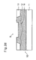
- FIG. 4 is a cross-sectional view of FIG. 3 taken along lines A–A′.
- the reference number 23 is an epitaxial layer playing a role of a substrate, and reference number 24 is a doping profile of a photodiode.
- FIG. 5 is an equivalent circuit of a photodiode.
- the disclosed methods can be applied to multi-transistor image sensor structures as well as a one-transistor image sensor structure.
- the method for making of shallow trench type pixel for CMOS image sensor can compensate reduction in the active area of a pixel using the area of the lateral wall of a shallow trench formed by etching the pixel area, although the design size of a pixel is reduced.
- the doping profile around the edge of the shallow trench is formed deeply toward the lateral wall of the STI layer, thereby having an effect of a reduction of recombination current.
- the foregoing disclosed methods for making a shallow trench type pixel for a CMOS image sensor substantially obviate one or more problems due to limitations and disadvantages of the related art.
- the disclosed methods include making a shallow trench type pixel, which can secure a minimum number of photoelectrons for processing video signals by increasing the active area of a pixel through forming a photodiode in the shape of a shallow trench in order to solve the problems due to a reduction in the number of photoelectrons according to a pixel shrinkage in a deep submicron level, i.e., a less than 0.25 ⁇ m technology for a CMOS image sensor.
Landscapes
- Solid State Image Pick-Up Elements (AREA)
Abstract
Description
Claims (6)
Applications Claiming Priority (2)
| Application Number | Priority Date | Filing Date | Title |
|---|---|---|---|
| KR10-2002-0036334 | 2002-06-27 | ||
| KR1020020036334A KR20040001201A (en) | 2002-06-27 | 2002-06-27 | Method of making shallow trench type pixel for cmos image sensor |
Publications (2)
| Publication Number | Publication Date |
|---|---|
| US20040043530A1 US20040043530A1 (en) | 2004-03-04 |
| US6982187B2 true US6982187B2 (en) | 2006-01-03 |
Family
ID=31973522
Family Applications (1)
| Application Number | Title | Priority Date | Filing Date |
|---|---|---|---|
| US10/606,693 Expired - Fee Related US6982187B2 (en) | 2002-06-27 | 2003-06-26 | Methods of making shallow trench-type pixels for CMOS image sensors |
Country Status (2)
| Country | Link |
|---|---|
| US (1) | US6982187B2 (en) |
| KR (1) | KR20040001201A (en) |
Families Citing this family (4)
| Publication number | Priority date | Publication date | Assignee | Title |
|---|---|---|---|---|
| KR100606914B1 (en) * | 2004-12-29 | 2006-08-01 | 동부일렉트로닉스 주식회사 | Method of forming an isolation region of a semiconductor device |
| KR100738183B1 (en) * | 2005-09-01 | 2007-07-10 | 매그나칩 반도체 유한회사 | CMOS image sensor having an active area and a butting contact and a method of manufacturing the same |
| US8278691B2 (en) * | 2008-12-11 | 2012-10-02 | Micron Technology, Inc. | Low power memory device with JFET device structures |
| CN104157661B (en) * | 2014-08-15 | 2017-11-10 | 北京思比科微电子技术股份有限公司 | A kind of manufacture method of cmos image sensor |
Citations (5)
| Publication number | Priority date | Publication date | Assignee | Title |
|---|---|---|---|---|
| US4536946A (en) * | 1982-12-13 | 1985-08-27 | Junichi Nishizawa | Method for fabricating semiconductor photodetector |
| US6177333B1 (en) | 1999-01-14 | 2001-01-23 | Micron Technology, Inc. | Method for making a trench isolation for semiconductor devices |
| US6329233B1 (en) * | 2000-06-23 | 2001-12-11 | United Microelectronics Corp. | Method of manufacturing photodiode CMOS image sensor |
| US6372603B1 (en) * | 2000-03-17 | 2002-04-16 | Taiwan Semiconductor Manufacturing Co., Ltd. | Photodiode with tightly-controlled junction profile for CMOS image sensor with STI process |
| US6500692B1 (en) | 1999-02-01 | 2002-12-31 | Micron Technology, Inc. | Method of making trench photosensor for a CMOS imager |
Family Cites Families (5)
| Publication number | Priority date | Publication date | Assignee | Title |
|---|---|---|---|---|
| JPS60124966A (en) * | 1983-12-10 | 1985-07-04 | Matsushita Electronics Corp | Manufacturing method of solid-state imaging device |
| JPH01123468A (en) * | 1987-11-06 | 1989-05-16 | Oki Electric Ind Co Ltd | Solid-state image sensing element |
| JPH1174499A (en) * | 1997-07-04 | 1999-03-16 | Toshiba Corp | Solid-state imaging device, manufacturing method thereof, and system using the solid-state imaging device |
| KR100298178B1 (en) * | 1998-06-29 | 2001-08-07 | 박종섭 | Photodiode in image sensorr |
| KR20020045451A (en) * | 2000-12-11 | 2002-06-19 | 박종섭 | Method for fabricating CMOS image sensor |
-
2002
- 2002-06-27 KR KR1020020036334A patent/KR20040001201A/en not_active Ceased
-
2003
- 2003-06-26 US US10/606,693 patent/US6982187B2/en not_active Expired - Fee Related
Patent Citations (5)
| Publication number | Priority date | Publication date | Assignee | Title |
|---|---|---|---|---|
| US4536946A (en) * | 1982-12-13 | 1985-08-27 | Junichi Nishizawa | Method for fabricating semiconductor photodetector |
| US6177333B1 (en) | 1999-01-14 | 2001-01-23 | Micron Technology, Inc. | Method for making a trench isolation for semiconductor devices |
| US6500692B1 (en) | 1999-02-01 | 2002-12-31 | Micron Technology, Inc. | Method of making trench photosensor for a CMOS imager |
| US6372603B1 (en) * | 2000-03-17 | 2002-04-16 | Taiwan Semiconductor Manufacturing Co., Ltd. | Photodiode with tightly-controlled junction profile for CMOS image sensor with STI process |
| US6329233B1 (en) * | 2000-06-23 | 2001-12-11 | United Microelectronics Corp. | Method of manufacturing photodiode CMOS image sensor |
Also Published As
| Publication number | Publication date |
|---|---|
| US20040043530A1 (en) | 2004-03-04 |
| KR20040001201A (en) | 2004-01-07 |
Similar Documents
| Publication | Publication Date | Title |
|---|---|---|
| KR100865839B1 (en) | Low dark current image sensors with epitaxial sic and/or carbonated channels for array transistors | |
| US10784303B2 (en) | Method of manufacturing a CMOS image sensor | |
| CN100583460C (en) | PIN diodes and methods for fabricating PIN diodes and forming semiconductor fin structures | |
| US6437417B1 (en) | Method for making shallow trenches for isolation | |
| CN104347645B (en) | Photodiode gate dielectric protective layer | |
| US20080057612A1 (en) | Method for adding an implant at the shallow trench isolation corner in a semiconductor substrate | |
| US20150115337A1 (en) | Semiconductor structure and manufacturing method thereof | |
| US7397100B2 (en) | Image sensor and method of manufacturing the same | |
| CN113629090A (en) | A pixel, an image sensor, a preparation method thereof, and an image acquisition device | |
| US20180182790A1 (en) | Method for manufacturing a semiconductor device | |
| US8460993B2 (en) | Method for fabricating CMOS image sensor with plasma damage-free photodiode | |
| US10026767B2 (en) | Semiconductor device and manufacturing method thereof | |
| US20020079518A1 (en) | Solid imaging device and production method thereof | |
| US8071417B2 (en) | Image sensor and fabrication method thereof | |
| US6982187B2 (en) | Methods of making shallow trench-type pixels for CMOS image sensors | |
| US20220367245A1 (en) | Shallow trench isolation (sti) structure for cmos image sensor | |
| US8048705B2 (en) | Method and structure for a CMOS image sensor using a triple gate process | |
| US20240063325A1 (en) | Method for forming semiconductor structure | |
| KR100708866B1 (en) | Manufacturing Method of Image Sensor | |
| US7732885B2 (en) | Semiconductor structures with dual isolation structures, methods for forming same and systems including same | |
| US7781253B2 (en) | Image sensor and method of manufacturing the same | |
| JP2017183668A (en) | Manufacturing method for solid-state image pickup device | |
| US20080124830A1 (en) | Method of manufacturing image sensor | |
| KR100766675B1 (en) | Image sensor manufacturing method for reducing dark signal | |
| US12284837B2 (en) | Backside illuminated image sensor and manufacturing method thereof |
Legal Events
| Date | Code | Title | Description |
|---|---|---|---|
| AS | Assignment |
Owner name: DONGBU ELECTRONICS CO., LTD., KOREA, REPUBLIC OF Free format text: ASSIGNMENT OF ASSIGNORS INTEREST;ASSIGNORS:JANG, HOON;LIM, KEUN HYUK;REEL/FRAME:014284/0906 Effective date: 20030627 |
|
| AS | Assignment |
Owner name: DONGBUANAM SEMICONDUCTOR, INC., KOREA, REPUBLIC OF Free format text: MERGER;ASSIGNOR:DONGBU SEMICONDUCTOR INC.;REEL/FRAME:016593/0667 Effective date: 20041221 |
|
| FEPP | Fee payment procedure |
Free format text: PAYOR NUMBER ASSIGNED (ORIGINAL EVENT CODE: ASPN); ENTITY STATUS OF PATENT OWNER: LARGE ENTITY Free format text: PAYER NUMBER DE-ASSIGNED (ORIGINAL EVENT CODE: RMPN); ENTITY STATUS OF PATENT OWNER: LARGE ENTITY |
|
| AS | Assignment |
Owner name: DONGBU ELECTRONICS CO., LTD., KOREA, REPUBLIC OF Free format text: CHANGE OF NAME;ASSIGNOR:DONGBU ANAM SEMICONDUCTORS, INC;REEL/FRAME:017718/0964 Effective date: 20060410 |
|
| FEPP | Fee payment procedure |
Free format text: PAYER NUMBER DE-ASSIGNED (ORIGINAL EVENT CODE: RMPN); ENTITY STATUS OF PATENT OWNER: LARGE ENTITY |
|
| FPAY | Fee payment |
Year of fee payment: 4 |
|
| FEPP | Fee payment procedure |
Free format text: PAYOR NUMBER ASSIGNED (ORIGINAL EVENT CODE: ASPN); ENTITY STATUS OF PATENT OWNER: LARGE ENTITY |
|
| REMI | Maintenance fee reminder mailed | ||
| LAPS | Lapse for failure to pay maintenance fees | ||
| STCH | Information on status: patent discontinuation |
Free format text: PATENT EXPIRED DUE TO NONPAYMENT OF MAINTENANCE FEES UNDER 37 CFR 1.362 |
|
| STCH | Information on status: patent discontinuation |
Free format text: PATENT EXPIRED DUE TO NONPAYMENT OF MAINTENANCE FEES UNDER 37 CFR 1.362 |
|
| FP | Lapsed due to failure to pay maintenance fee |
Effective date: 20140103 |