US6958526B2 - Electronic structures with reduced capacitance - Google Patents
Electronic structures with reduced capacitance Download PDFInfo
- Publication number
- US6958526B2 US6958526B2 US10/766,249 US76624904A US6958526B2 US 6958526 B2 US6958526 B2 US 6958526B2 US 76624904 A US76624904 A US 76624904A US 6958526 B2 US6958526 B2 US 6958526B2
- Authority
- US
- United States
- Prior art keywords
- dielectric material
- region
- sicoh
- electronic structure
- sicoh dielectric
- Prior art date
- Legal status (The legal status is an assumption and is not a legal conclusion. Google has not performed a legal analysis and makes no representation as to the accuracy of the status listed.)
- Expired - Lifetime
Links
- 239000000203 mixture Substances 0.000 claims abstract description 39
- 239000004020 conductor Substances 0.000 claims abstract description 37
- 230000015556 catabolic process Effects 0.000 claims abstract description 31
- 239000003989 dielectric material Substances 0.000 claims description 65
- 229910052799 carbon Inorganic materials 0.000 claims description 64
- OKTJSMMVPCPJKN-UHFFFAOYSA-N Carbon Chemical compound [C] OKTJSMMVPCPJKN-UHFFFAOYSA-N 0.000 claims description 44
- 239000003990 capacitor Substances 0.000 claims description 34
- 229910052760 oxygen Inorganic materials 0.000 claims description 20
- 229910052710 silicon Inorganic materials 0.000 claims description 19
- 229910052739 hydrogen Inorganic materials 0.000 claims description 10
- 230000004888 barrier function Effects 0.000 claims description 8
- 230000007704 transition Effects 0.000 claims description 7
- QVGXLLKOCUKJST-UHFFFAOYSA-N atomic oxygen Chemical compound [O] QVGXLLKOCUKJST-UHFFFAOYSA-N 0.000 claims description 5
- 239000001301 oxygen Substances 0.000 claims description 5
- 229910052757 nitrogen Inorganic materials 0.000 claims description 3
- 239000000654 additive Substances 0.000 claims 2
- 230000000996 additive effect Effects 0.000 claims 2
- 238000000034 method Methods 0.000 abstract description 5
- 239000010408 film Substances 0.000 description 29
- 239000000758 substrate Substances 0.000 description 26
- 238000004804 winding Methods 0.000 description 20
- 239000000463 material Substances 0.000 description 19
- 230000003071 parasitic effect Effects 0.000 description 16
- 239000012528 membrane Substances 0.000 description 14
- 239000010409 thin film Substances 0.000 description 12
- 239000010949 copper Substances 0.000 description 7
- 238000002161 passivation Methods 0.000 description 7
- VYPSYNLAJGMNEJ-UHFFFAOYSA-N Silicium dioxide Chemical compound O=[Si]=O VYPSYNLAJGMNEJ-UHFFFAOYSA-N 0.000 description 6
- 230000001939 inductive effect Effects 0.000 description 6
- 238000002955 isolation Methods 0.000 description 6
- 230000008878 coupling Effects 0.000 description 5
- 238000010168 coupling process Methods 0.000 description 5
- 238000005859 coupling reaction Methods 0.000 description 5
- 230000009977 dual effect Effects 0.000 description 5
- 239000002184 metal Substances 0.000 description 5
- 229910052751 metal Inorganic materials 0.000 description 5
- 239000002243 precursor Substances 0.000 description 5
- XLYOFNOQVPJJNP-UHFFFAOYSA-N water Substances O XLYOFNOQVPJJNP-UHFFFAOYSA-N 0.000 description 5
- 238000010586 diagram Methods 0.000 description 4
- 230000005684 electric field Effects 0.000 description 4
- 230000000873 masking effect Effects 0.000 description 4
- 230000003647 oxidation Effects 0.000 description 4
- 238000007254 oxidation reaction Methods 0.000 description 4
- 229910052681 coesite Inorganic materials 0.000 description 3
- 229910052906 cristobalite Inorganic materials 0.000 description 3
- -1 cyclic siloxanes Chemical class 0.000 description 3
- 229920000642 polymer Polymers 0.000 description 3
- 239000000377 silicon dioxide Substances 0.000 description 3
- 229910052682 stishovite Inorganic materials 0.000 description 3
- 229910052905 tridymite Inorganic materials 0.000 description 3
- 239000004642 Polyimide Substances 0.000 description 2
- 230000008901 benefit Effects 0.000 description 2
- 230000008859 change Effects 0.000 description 2
- 239000000696 magnetic material Substances 0.000 description 2
- 229920001721 polyimide Polymers 0.000 description 2
- 230000008569 process Effects 0.000 description 2
- RYGMFSIKBFXOCR-UHFFFAOYSA-N Copper Chemical compound [Cu] RYGMFSIKBFXOCR-UHFFFAOYSA-N 0.000 description 1
- 229910052581 Si3N4 Inorganic materials 0.000 description 1
- HMDDXIMCDZRSNE-UHFFFAOYSA-N [C].[Si] Chemical compound [C].[Si] HMDDXIMCDZRSNE-UHFFFAOYSA-N 0.000 description 1
- 238000010521 absorption reaction Methods 0.000 description 1
- PNEYBMLMFCGWSK-UHFFFAOYSA-N aluminium oxide Inorganic materials [O-2].[O-2].[O-2].[Al+3].[Al+3] PNEYBMLMFCGWSK-UHFFFAOYSA-N 0.000 description 1
- 229910000808 amorphous metal alloy Inorganic materials 0.000 description 1
- 239000003575 carbonaceous material Substances 0.000 description 1
- 239000012159 carrier gas Substances 0.000 description 1
- 229910052802 copper Inorganic materials 0.000 description 1
- 229910052593 corundum Inorganic materials 0.000 description 1
- 238000005516 engineering process Methods 0.000 description 1
- 239000012212 insulator Substances 0.000 description 1
- 229910044991 metal oxide Inorganic materials 0.000 description 1
- 150000004706 metal oxides Chemical class 0.000 description 1
- 230000004048 modification Effects 0.000 description 1
- 238000012986 modification Methods 0.000 description 1
- 150000001282 organosilanes Chemical class 0.000 description 1
- 230000001590 oxidative effect Effects 0.000 description 1
- 238000000059 patterning Methods 0.000 description 1
- 238000000623 plasma-assisted chemical vapour deposition Methods 0.000 description 1
- 230000001681 protective effect Effects 0.000 description 1
- 239000004065 semiconductor Substances 0.000 description 1
- HQVNEWCFYHHQES-UHFFFAOYSA-N silicon nitride Chemical compound N12[Si]34N5[Si]62N3[Si]51N64 HQVNEWCFYHHQES-UHFFFAOYSA-N 0.000 description 1
- PBCFLUZVCVVTBY-UHFFFAOYSA-N tantalum pentoxide Inorganic materials O=[Ta](=O)O[Ta](=O)=O PBCFLUZVCVVTBY-UHFFFAOYSA-N 0.000 description 1
- CZDYPVPMEAXLPK-UHFFFAOYSA-N tetramethylsilane Chemical compound C[Si](C)(C)C CZDYPVPMEAXLPK-UHFFFAOYSA-N 0.000 description 1
- 229920001187 thermosetting polymer Polymers 0.000 description 1
- PQDJYEQOELDLCP-UHFFFAOYSA-N trimethylsilane Chemical compound C[SiH](C)C PQDJYEQOELDLCP-UHFFFAOYSA-N 0.000 description 1
- 229910001845 yogo sapphire Inorganic materials 0.000 description 1
Images


Classifications
-
- H—ELECTRICITY
- H01—ELECTRIC ELEMENTS
- H01L—SEMICONDUCTOR DEVICES NOT COVERED BY CLASS H10
- H01L27/00—Devices consisting of a plurality of semiconductor or other solid-state components formed in or on a common substrate
- H01L27/02—Devices consisting of a plurality of semiconductor or other solid-state components formed in or on a common substrate including semiconductor components specially adapted for rectifying, oscillating, amplifying or switching and having at least one potential-jump barrier or surface barrier; including integrated passive circuit elements with at least one potential-jump barrier or surface barrier
- H01L27/04—Devices consisting of a plurality of semiconductor or other solid-state components formed in or on a common substrate including semiconductor components specially adapted for rectifying, oscillating, amplifying or switching and having at least one potential-jump barrier or surface barrier; including integrated passive circuit elements with at least one potential-jump barrier or surface barrier the substrate being a semiconductor body
- H01L27/08—Devices consisting of a plurality of semiconductor or other solid-state components formed in or on a common substrate including semiconductor components specially adapted for rectifying, oscillating, amplifying or switching and having at least one potential-jump barrier or surface barrier; including integrated passive circuit elements with at least one potential-jump barrier or surface barrier the substrate being a semiconductor body including only semiconductor components of a single kind
-
- H—ELECTRICITY
- H01—ELECTRIC ELEMENTS
- H01F—MAGNETS; INDUCTANCES; TRANSFORMERS; SELECTION OF MATERIALS FOR THEIR MAGNETIC PROPERTIES
- H01F17/00—Fixed inductances of the signal type
- H01F17/0006—Printed inductances
-
- H—ELECTRICITY
- H01—ELECTRIC ELEMENTS
- H01F—MAGNETS; INDUCTANCES; TRANSFORMERS; SELECTION OF MATERIALS FOR THEIR MAGNETIC PROPERTIES
- H01F27/00—Details of transformers or inductances, in general
- H01F27/34—Special means for preventing or reducing unwanted electric or magnetic effects, e.g. no-load losses, reactive currents, harmonics, oscillations, leakage fields
Definitions
- This invention relates to passive components integrated on an integrated circuit chip, an integrated circuit carrier, and a circuit board.
- This invention also relates to low capacitance multilayer circuit boards, to interconnect structures for high speed microprocessors, to application specific integrated circuits (ASICs), and to other high speed integrated circuits (IC's).
- the structures of this invention include a dielectric material having a low dielectric constant, very high breakdown field, and excellent (air barrier) passivation properties.
- the invention also describes an improved thin film form of the dielectric material that is useful in some of the inventive electronic structures.
- Prior art inductor structures used in RF and microwave circuits are commonly isolated from ground using SiO 2 which has a dielectric constant (k) of 4 to 4.2.
- Prior art inductors maybe passivated with a polymer dielectric (e.g. Polyimide which has a dielectric constant (k) or about 2.9
- Prior art transformer structures are commonly isolated internally using SiO 2 with a dielectric constant (k) of 4 to 4.2 between adjacent conductors or turns in the winding and between windings.
- Prior art multilayer circuit boards commonly are built with a polymer dielectric that absorbs water and has a relatively low breakdown field.
- a multilayer circuit board structure is needed with low capacitance between metal layers, such as using a dielectric material with a low dielectric constant, a high breakdown voltage and very low water absorption.
- Cu interconnect structures with low-k dielectric are known.
- An example dual damascene type structure is described in R. Goldblatt et al, “A high performance 0.13 micron Copper BEOL technology with low k dielectric”, Proceedings of IITC, 2000. These structures may have high leakage current between the Cu lines, especially as the spacing between the lines is reduced below 180 nm.
- Prior art capacitor structures used in RE and microwave circuits are commonly isolated from ground using SiO 2 which has a dielectric constant (k) of 4 to 4.2, or another material with still larger k.
- the capacitors may be passivated with a polymer dielectric (e.g. Polyimide) which has a dielectric constant (k) or about 2.9.
- a polymer dielectric e.g. Polyimide
- the invention provides electronic structures that have superior properties, i.e. reduced parasitic capacitance and improved reliability.
- the structures of this invention contain a dielectric material “SiCOH” having a low dielectric constant, very low leakage current, high breakdown field, and excellent passivation (air barrier) properties.
- inductors having reduced capacitance both within the inductive device and parasitic capacitance between the device and ground, transformers having reduced capacitance within the device, low capacitance circuit boards, and reliable capacitors having a low capacitance.
- the invention provides a spiral, toroidal or membrane inductor having a low capacitance within the inductive structure, and a low capacitance between the inductor and ground.
- these inductors must be reliable for long life in integrated circuits such as in mobile applications.
- the invention provides a transformer having a low internal capacitance between two conductive windings. Also, the transformer should have a low capacitance to the substrate or ground. In addition, the transformer must be reliable. These properties are obtained in a transformer containing a layer of SiCOH dielectric material between the 2 windings. Said SiCOH dielectric has a low dielectric constant, a high breakdown voltage, a low leakage current, and low oxygen and water permeation.
- An improved low-k dielectric plus Cu interconnect structure (such as dual damascene type) for high speed microprocessors and ASIC's according to the invention is also described.
- the invention provides a low-k Cu interconnect structure with a dielectric having a low dielectric constant (k) and simultaneously a low leakage current between Cu lines where the lines are spaced less than 180 nm apart.
- the invention provides an interdigital capacitor having a low parasitic capacitance and excellent reliability. This is obtained in a capacitor structure in which the SiCOH dielectric material has a low dielectric constant, a high breakdown voltage, a low leakage current, and low oxygen and water permeation, is used to isolate the structure from the substrate.
- a low leakage current is defined here as approximately less than 10 nAmp/cm2 at an applied field of 1 MV/cm. Further, this material is a reliable barrier to O2 and H2O permeation.
- This invention improves on prior art structures by reducing the parasitic capacitance of the structures.
- the integrated devices also have excellent electrical isolation (low leakage).
- the SiCOH dielectric material also called “carbon-doped oxide” exhibits a very high breakdown voltage, from 4.5 to 10 MV/cm, and a low leakage current and dielectric constant less than 3.5 when prepared according to the procedures described here and when the material has the atomic composition specified herein.
- FIG. 1A is a top view of one embodiment of the invention showing a spiral inductor.
- FIG. 1B is a cross section view along the lines 1 B— 1 B of FIG. 1 A.
- FIG. 1C is a schematic circuit of an electrical model of the inductor shown in FIG. 1 .
- FIG. 1D is a top view of an alternated embodiment of the invention showing a rectangular spiral inductor.
- FIG. 1E is a cross section view along the lines 1 E— 1 E of FIG. 1 D.
- FIG. 2A is a cross section view along the lines 2 A— 2 A of FIG. 2C showing a membrane inductor structure of this invention.
- FIG. 2B is a cross section view as shown in FIG. 2A with an interconnection layer added on top.
- FIG. 2C is a top view of a membrane inductor.
- FIG. 3A is a perspective view of a transformer.
- FIG. 3B is a top view of FIG. 3C of a transformer structure of this invention.
- FIG. 3C is a cross section view along the lines 3 C— 3 C of FIG. 3 B.
- FIG. 4 is a cross section view of the first multilayer circuit board structure of this invention.
- FIG. 5 is a cross section view of a first multilayer circuit board structure of this invention.
- FIG. 6 is a cross section view of a low-k interconnect structure of the dual damascene type of this invention.
- FIG. 7A is a top view of an interdigital capacitor structure of this invention.
- FIG. 7B is a cross section view along the lines 7 B— 7 B of FIG. 7 A.
- FIG. 7C is a schematic circuit of an electrical model of the capacitor shown in FIGS. 7A and 7B where C 1 is reduced due to use of the low k dielectric.
- FIG. 7D is a cross section view of an alternate embodiment showing a parallel plate capacitor.
- FIG. 8 is a graph of the current per unit area versus electric field of the thick film SiCOH dielectric material of this invention.
- FIG. 9A is a graph of the current per unit area versus field of the thin film SiCOH dielectric material of this invention.
- FIG. 9B is a graph of the percent of occurrence of breakdown versus breakdown electric field of the thin film SiCOH dielectric material of this invention.
- FIGS. 10A and 10B are graphs of the carbon content versus depth in a layer of low k SiCOH dielectric of the invention.
- an inductor In an RF or microwave circuit, an inductor is commonly needed. Power consumption through current leakage from the inductor to the substrate should be minimized to use the circuit in a mobile phone or other mobile battery powered device. Parasitic capacitance between the inductor and the substrate is also a problem, and this capacitance is worse at higher frequencies. Commonly, the maximum operating frequency of an inductor is limited by parasitic capacitance.
- FIG. 1 is a schematic drawing of the spiral inductor structure of this invention.
- FIG. 1A is a top view showing the layout of said inductor.
- FIG. 1B is a section view through Plane B, showing the layers of said inductor in cross-section.
- FIG. 1C is a schematic circuit diagram to illustrate the use of the structure of FIGS. 1A and 1B in an RF or microwave circuit.
- substrate 1 contains a layer of patterned conductor formed within dielectric layer 2 .
- One of the conductors, 3 is shown.
- a layer of the SiCOH dielectric, 4 is located on the patterned conductors.
- One via contact to the inductor, 6 is located within the SiCOH dielectric layer.
- a spiral inductor structure, 5 is located within the SiCOH dielectric layer.
- a protective (passivation) layer of the SiCOH dielectric, 11 Surrounding the inductor structure is a protective (passivation) layer of the SiCOH dielectric, 11 .
- the SiCOH dielectric layer serves to isolate the inductor structure from the substrate, providing a low dielectric constant and low leakage isolation.
- the C 1 and C 2 parasitic capacitances are made as small as possible through the use of SiCOH dielectric as layer 4 .
- the internal capacitance, C 3 , of the inductor is made as small as possible through the use of SiCOH dielectric as layer 11 .
- an alternative shape of the inductor may be used in the inventive structure, including a toroidal shape or the type of shape shown in FIG. 2 .
- the SiCOH dielectric layers, 4 and 11 , in FIG. 1B has the preferred atomic composition Range H 30-35%, C 12-18%, Si 18-22%, O 30-35%, and more generally the composition range may be H 25-55%, C 10-40%, Si 10-25%, O 10-25%.
- the SiCOH dielectric of the present invention includes the precursors described in U.S. Pat. No. 6,147,009 and trimethylsilane or tetramethylsilane and an oxidizing precursor, for example O 2 , N 2 O, CO 2 , etc. and also includes other organosilane precursors.
- This film is typically 0.5 micron or greater in thickness, and has a measured current versus electric field curve similar to that shown in FIG. 8 below, and has a breakdown field of greater than 4.5 MV/cm, and a dielectric constant of less than 3.5, and commonly less than 3.
- the composition is not uniform throughout the film thickness.
- a “graded” composition may be to create a dense region containing less H and C at the outer film surface to form a non-permeable barrier region.
- a second example is to improve adhesion at an interface by changing the composition at that interface.
- the film is formed in a multilayer (nanolaminate) form with sub-layers in the thin film, for example 3 sub-layers.
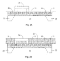
- FIG. 2 is a schematic drawing of the membrane inductor structure of this invention, in which a membrane is made of the SiCOH dielectric, which has both a low dielectric constant and excellent insulator properties.
- FIG. 2A is a section view of said inductor with 1 dielectric layer as the supporting membrane under the inductor.
- a layer of the SiCOH dielectric, 21 has been formed as a membrane by removing a sacrificial material (not shown). Regions of the substrate, 22 , remain supporting the membrane.
- conductors 25 and 25 ′, to connect the inductor.
- windings 23 .
- a layer of the SiCOH dielectric, 26 has been deposited to protect and passivate the structure.
- the conductor layer 24 is atop the passivation layer, 26 , making electrical contact to one end of the windings.
- the C 1 and C 2 parasitic capacitances are minimized through the use of SiCOH dielectric membrane, 21 , supported over an air gap 20 .
- the internal capacitance, C 3 , of the inductor is made as small as possible through the use of SiCOH dielectric as layer 26 , which protects the structure.
- an alternative shape of the inductor may be used in the inventive structure, including a torroidal shape or the spiral shape shown in FIG. 1 .
- SiCOH dielectric layers, 21 and 26 , In FIG. 2 have the same characterisitics and composition described above in reference to Example 1.
- Transformer structures integrated on an IC, or on an IC carrier (“flip-chip”) are commonly useful. Capacitive coupling within the transformer (between the windings) consumes power and limits the frequency of operation. A low capacitive coupling between the windings would be desirable, for example a dielectric material with low dielectric constant (low k). Commonly, the dielectric between the 2 windings of the transformer may undergo dielectric breakdown. A transformer dielectric with low k and with a high breakdown voltage would be desirable.
- FIG. 3A shows a perspective view of a transformer structure according to the invention.
- FIG. 3B is a top view
- FIG. 3C is a section view
- a top winding, 34 is patterned in a convenient closed loop shape.
- Conductor regions 35 carry current to said top winding.
- a layer of SiCOH dielectric, 33 is underneath said top winding.
- Conductor regions 32 carry current to a lower winding 31 shown in FIG. 3C.
- a magnetic material 36 which may be permanent magnetic material is located within the closed loop of said top winding and said lower winding.
- FIG. 3C is a cross section view through along the lines 3 C— 3 C of FIG. 3 B. Atop substrate 1 , is located a lower winding, 31 . The SiCOH dielectric, 33 , is seen in cross section between patterned conductors 31 and 34 .
- the transformer structure of this invention may contain a discontinuous layer of SiCOH dielectric underneath the upper winding 34 , so that said upper winding is supported in regions by said layer of SiCOH dielectric, and in other regions is not supported such as by an air bridge or air gaps.
- the SiCOH dielectric layer, 33 , in FIG. 3 has the same characterisitics and composition described above in reference to Example 1.
- FIG. 4 is a cross section view showing the layers of the first circuit board substructure of this invention, using a thick film of the SiCOH material.
- an insulating substrate, 41 supports a first conductor layer that is patterned to form a plurality of first conductors, 43 . Separating said plurality of first conductors, 43 , is a dielectric, 42 . Atop said layers is a SiCOH dielectric layer, 44 , seen in cross section. Atop said SiCOH layer is a second conductor layer that is patterned to form a plurality of second conductors, 47 . Separating said plurality of second conductors, 47 , is a dielectric, 46 . Within said SiCOH layer is a plurality of connectors (vias), 45 , making selected electrical contact between conductors 43 and 47 .
- a multilayer circuit board structure according to the invention may contain one substructure or a plurality of substructures, meaning the substructure of FIG. 4 may be repeated to form a multilayer circuit board structure.
- the SiCOH dielectric layer, 44 , in FIG. 4 has the same characterisitics and composition described above in reference to Example 1.
- FIG. 5 is a cross section view showing the layers of the second circuit board substructure of this invention, using a thick film of the SiCOH material.
- an insulating substrate, 51 supports a first conductor layer that is patterned to form a plurality of first conductors, 53 .
- a SiCOH dielectric layer, 52 seen in cross section.
- a second conductor layer that is patterned to form a plurality of second conductors, 57 .
- Within said SiCOH layer is a plurality of connectors (vias), 55 , making selected electrical contact between conductors 53 and 57 .
- a multilayer circuit board structure according to the invention may contain one substructure or a plurality of substructures, meaning the substructure of FIG. 5 may be repeated to form a multilayer circuit board structure.
- the SiCOH dielectric layer, 52 , in FIG. 5 has the same characterisitics and composition described above in reference to Example 1.
- FIG. 6 is a section view showing the layers of the low-k interconnect structure of the dual damascene type, of this invention made in a polymeric organic thermoset dielectric and using the SiCOH dielectric material formed as a thin film (thickness>about 30-50 nm, and less than 100 nm.). As a hardmask patterning/CMP-stop layer.
- patterned metal conductors 68 which are formed within a low-k dielectric, 61 .
- Atop the dielectric 61 is a second layer of low-k dielectric 65 and atop the low-k dielectric 65 is a masking/cmp-stop layer, 63 .
- the metal conductors, 62 are formed.
- said masking/cmp-stop layer, 63 is comprised of the thin film form of the SiCOH dielectric having a thickness from 20-100 nm, and preferably 30-60 nm.
- the “post-CMP Cap” layer, 64 Atop the masking/cmp-stop layer 63 , and the metal conductors, 62 , is the “post-CMP Cap” layer, 64 .
- said post CMP-cap layer is an amorphous alloy of Si, C, H or Si, N, C H.
- Atop the “post-CMP Cap” layer, 64 is a third layer of low-k dielectric 65 and atop the low-k dielectric is a masking/cmp-stop layer, 67 .
- Metal conductors, 66 are formed within the layers 65 and 67 .
- the SiCOH dielectric layer 65 and 61 in FIG. 6 has the preferred atomic composition H 30-35%, C 13-17%, Si 20-26%, O 25-32%.
- the measured current versus electric filed curve is similar to that shown in FIG. 9 below, and a breakdown field of greater than 6 MV/cm is measured (see FIG. 9 ), and a dielectric constant of less than 3.5.
- the composition may be H 25-55%, C 10-40%, Si 10-30%, O 10-35%.
- the composition is not uniform throughout the film thickness, and a “graded” composition is used for example to improve adhesion at an interface.
- the film is formed in a multilayer (nanolaminate) form with sub-layers in the thin film, for example 3 sub-layers.
- FIG. 7 contains schematic drawings of the capacitor structures of this invention, said structures containing SiCOH dielectric layers for: 1) isolation from the substrate, and 2) protection (passivation) against air oxidation. (Not for the capacitor dielectric)
- FIG. 7A is a top view of an interdigital capacitor according to this invention.
- the interdigital structure is one example layout of a capacitor according to the invention.
- FIG. 7B is a section view showing the layers of said capacitor in cross-section.
- FIG. 7C is a schematic circuit diagram to illustrate the use of the capacitor of FIGS. 7A and 7B in an RF or microwave circuit.
- FIG. 7D is a section view showing the layers of a parallel plate capacitor according to the invention.
- FIG. 7A which is a top view, a capacitor structure, 75 , contains a conductor layer that is patterned into 2 electrodes, 77 and 78 , which electrodes are shown with an interdigitated structure to increase the capacitor area. Other structures for the 2 electrodes are also possible within this invention.
- a via contact, 76 to one of the electrodes is shown.
- FIG. 7B is a section view of said capacitor in which a substrate, 71 , contains a dielectric layer 72 and a lower conductor, 73 , within said dielectric.
- a layer of the SiCOH dielectric, 74 is atop the conductor layer. Layer 74 provides low capacitance isolation from the substrate.
- a single via contact, 76 passes through the SiCOH dielectric and makes contact to the 1st electrode, 77 .
- the second electrode and a second via contact to said electrode are not shown in the section view of 7 B.
- the electrodes are made by a damascene process within the capacitor dielectric, 79 .
- a layer of the SiCOH dielectric, 80 may optionally be located atop the capacitor structure to provide protection (passivation) against air oxidation.
- FIG. 7C is a schematic circuit diagram, in which the parasitic capacitance between the structure 75 and the substrate 71 is shown as C 1 .
- C 1 is reduced to a minimum value by a low k dielectric (SiCOH) as layer 74 .
- the R, L, and C of FIG. 7C are the resistance, inductance and capacitance, respectively, of the structure shown in FIGS. 7A and 7B .
- FIG. 7D An alternative capacitor of this invention is shown in cross-section in FIG. 7D , a parallel plate type capacitor.
- a substrate, 91 contains a layer of the SiCOH dielectric, 94 , atop the substrate.
- Layer 94 provides low capacitance isolation from the substrate.
- a single via contact, 96 passes through the SiCOH dielectric and makes contact to the 1st electrode, 97 , which is formed within a dielectric layer 99 .
- the capacitor dielectric, 98 may be a high k metal oxide (Ta 2 O 5 , Al 2 O 3 , etc.), or silicon nitride, or another dielectric.
- the second electrode 101 and a via, 102 contacting said electrode are shown.
- the second electrode is formed within a dielectric layer 100 .
- C 1 represents the parasitic capacitance between the capacitor structure and the substrate 91 , and C 1 is reduced to a minimum value by a low k dielectric (SiCOH) as layer 94 .
- SiCOH low k dielectric
- the SiCOH dielectric layer, 94 has the same characterisitics and composition described above in reference to to Example 1.
- FIG. 8 is a current vs. Field plot of the thick film SiCOH dielectric material of this invention. Dielectric breakdown, 105 , is seen at an applied field, E, of between 4.5 and 5 MV/cm. The leakage current, 106 , at 1 MV/cm applied field is less than 1 nanoAmp/cm2.
- FIG. 8 shows this material is an exceptionally stable dielectric having superior properties compared to other Low-k dielectrics.
- the high breakdown field and low leakage current and low dielectric constant are not expected, based on other Low-k dielectrics.
- These properties make the SiCOH dielectric film of FIG. 8 especially suited as an isolation dielectric for use in many electronic structures. For example, inductors, capacitors and resistors may all be isolated from a substrate using this material, with new and unexpected gains in high frequency performance.
- FIG. 9A is a current versus electric field plot for the thin film SiCOH dielectric material of this invention.
- FIG. 9B is a plot of the % of capacitors having a specific Breakdown Field plotted versus said field, so is a Breakdown distribution plot, for the thin film SiCOH dielectric material of this invention.
- the data in FIG. 9 was measured from films having the composition H 32%, C 16%, Si 22%, O 30%.
- the black curve 109 is measured from a film 50 nm thick, and the gray curve 112 is from a film 37 nm thick. Both curves are from a capacitor having approximately 0.05 cm 2 area. Current density (per 1 cm 2 ) is then 20 ⁇ higher than the current values plotted.
- the black curve 109 from the 50 nm film has a leakage current at 1 MV/cm field, 110 , less than 1 nA/cm 2 .
- Dielectric breakdown, 111 for this film is seen near 10 MV/cm applied field.
- the gray curve 112 from the 37 nm film has a leakage current at 1 MV/cm field, 113 , of About 2 nA/cm 2 . Dielectric breakdown, 114 , for this film is seen near 11 MV/cm applied field.
- FIG. 9B summarizes the Breakdown field measured on 64 capacitors for the thin film SiCOH dielectric material of this invention, and is called a Breakdown distribution plot.
- the black curve 115 from the 50 nm film has dielectric breakdown mainly above 10 MV/cm applied field. Some capacitors break at lower field, 116 , between 8 and 10 MV/cm.
- the gray curve 117 from the 37 nm film has Dielectric breakdown greater than 9 MV/cm applied field, and the trend is similar to curve 115 for most of the capacitors tested.
- the very high breakdown field seen in FIG. 9 for both films (50 and 37 nm) shows this material is an exceptionally stable dielectric having superior properties compared to other Low-k dielectrics.
- the high breakdown field and low leakage current and low dielectric constant are not expected, based on other Low-k dielectrics.
- These properties make the SICOH dielectric film of FIG. 9 very well suited for use in many electronic structures, for example the transformer of FIG. 3 and the interconect structure of FIG. 6 .
- the desirable bulk properties of the SiCOH dielectric may lead to poor adhesion at an interface, or the film may be chemically changed by a process step when fabricating the inventive structures.
- use of layers that contain little or no Carbon is recommended. Said layers have the properties of deposited SiOxide which is a common material in the art.
- a graded composition layer of the SiCOH dielectric material may be used according to this invention. Two examples of a graded composition layer of the SiCOH dielectric material are shown in FIG. 10 .
- FIG. 10A illustrates the first graded Carbon layer of the SiCOH dielectric material of this invention, in which 3 different carbon contents may be used in different zones of a dielectric layer.
- FIG. 10A is a plot of the atomic percent Carbon in the SiCOH dielectric versus depth into the dielectric layer.
- the dashed line shows one implementation of the first graded Carbon layer of this invention, said dashed line marking 3 distinct zones ( 121 , 123 , 124 ) of the SiCOH dielectric film according to the invention.
- Region 121 is a low Carbon zone having properties similar to Si Oxide near the surface of the layer (near zero depth).
- Region 122 is an abrupt transition region to the typical SiCOH composition, region 123 , according to the invention.
- Region 123 has the atomic composition and properties given above in the Examples using the SiCOH dielectric.
- Region 122 ′ is a second abrupt transition region, to a low Carbon region, 124 , which also has properties similar to Si Oxide.
- the solid line shows a second implementation of the first graded Carbon layer of this invention, said solid line marking 3 distinct zones ( 126 , 127 , 128 ) of the SiCOH dielectric film according to the invention, with a continuous change in carbon content.
- Region 126 is a zone near the surface of the layer (near zero depth) in which the carbon concentration changes from low to high.
- the typical SiCOH composition (carbon content) is shown as region 127 , according to the invention.
- Region 127 has the atomic composition and properties given above in Examples 1-7.
- Region 128 is a zone near the bottom interface of the layer in which the carbon concentration changes from high to low.
- FIG. 10B illustrates the second graded Carbon layer of the SiCOH dielectric material of this invention, in which 2 different carbon contents may be used in two zones of a dielectric layer.
- FIG. 10B is a plot of the atomic percent Carbon in the SiCOH dielectric versus depth into the dielectric layer.
- the dashed line shows one implementation of the second graded Carbon layer of this invention, said dashed line marking 2 distinct zones ( 131 , 133 ,) of the SiCOH dielectric film according to the invention.
- Region 131 is a low Carbon zone near the surface of the layer (near zero depth), said zone having properties similar to Si Oxide.
- Region 132 is an abrupt transition region to the typical SiCOH composition, region 133 , according to the invention.
- Region 133 has the atomic composition and properties given above in Examples 1-7.
- the solid line shows a second implementation of the second graded Carbon layer of this invention, marking 2 distinct zones ( 134 , 133 ) of the SiCOH dielectric film according to the invention, with a continuous change in carbon content.
- Region 134 is a zone near the surface of the layer (near zero depth) in which the carbon concentration changes from low to high.
- the typical SiCOH composition (carbon content) is shown as region 133 , according to the invention.
- Region 133 has the atomic composition and properties given above in Examples 1-7.
- Region 131 or 134 (low carbon concentration) has a low carbon content, a high density, and hence superior air barrier properties for protection against oxidation compared to (zone 133 ) the SiCOH material.
- Capacitor, inductor and transformer structures of this invention have been described in detail.
- thin film resistor structures may also be separated from a substrate by a layer of the SiCOH dielectric material. These structures have a reduced parasitic capacitance compared to prior art thin film resistor structures, and are within the scope of this invention.
- Other structures may be made using the SiCOH dielectric to isolate the structure from the substrate with this invention, reducing parasitic capacitance and hence increasing the frequency of operation.
- this material is an effective protection (passivation) layer against air oxidation.
- the high breakdown field and low leakage current and low dielectric constant and air barrier properties of the SiCOH dielectric material are a new, unexpected combination of properties.
Landscapes
- Engineering & Computer Science (AREA)
- Power Engineering (AREA)
- Microelectronics & Electronic Packaging (AREA)
- Physics & Mathematics (AREA)
- Condensed Matter Physics & Semiconductors (AREA)
- General Physics & Mathematics (AREA)
- Computer Hardware Design (AREA)
- Internal Circuitry In Semiconductor Integrated Circuit Devices (AREA)
- Semiconductor Integrated Circuits (AREA)
Abstract
Description
Claims (22)
Priority Applications (1)
| Application Number | Priority Date | Filing Date | Title |
|---|---|---|---|
| US10/766,249 US6958526B2 (en) | 2001-01-12 | 2004-01-27 | Electronic structures with reduced capacitance |
Applications Claiming Priority (3)
| Application Number | Priority Date | Filing Date | Title |
|---|---|---|---|
| US26129201P | 2001-01-12 | 2001-01-12 | |
| US10/045,711 US6737727B2 (en) | 2001-01-12 | 2002-01-14 | Electronic structures with reduced capacitance |
| US10/766,249 US6958526B2 (en) | 2001-01-12 | 2004-01-27 | Electronic structures with reduced capacitance |
Related Parent Applications (1)
| Application Number | Title | Priority Date | Filing Date |
|---|---|---|---|
| US10/045,711 Continuation US6737727B2 (en) | 2001-01-12 | 2002-01-14 | Electronic structures with reduced capacitance |
Publications (2)
| Publication Number | Publication Date |
|---|---|
| US20040188674A1 US20040188674A1 (en) | 2004-09-30 |
| US6958526B2 true US6958526B2 (en) | 2005-10-25 |
Family
ID=26723106
Family Applications (2)
| Application Number | Title | Priority Date | Filing Date |
|---|---|---|---|
| US10/045,711 Expired - Lifetime US6737727B2 (en) | 2001-01-12 | 2002-01-14 | Electronic structures with reduced capacitance |
| US10/766,249 Expired - Lifetime US6958526B2 (en) | 2001-01-12 | 2004-01-27 | Electronic structures with reduced capacitance |
Family Applications Before (1)
| Application Number | Title | Priority Date | Filing Date |
|---|---|---|---|
| US10/045,711 Expired - Lifetime US6737727B2 (en) | 2001-01-12 | 2002-01-14 | Electronic structures with reduced capacitance |
Country Status (2)
| Country | Link |
|---|---|
| US (2) | US6737727B2 (en) |
| TW (1) | TWI269471B (en) |
Cited By (7)
| Publication number | Priority date | Publication date | Assignee | Title |
|---|---|---|---|---|
| US20060046520A1 (en) * | 2004-09-01 | 2006-03-02 | Applied Materials, Inc. | Method to deposit functionally graded dielectric films via chemical vapor deposition using viscous precursors |
| US20070173070A1 (en) * | 2006-01-26 | 2007-07-26 | Mei-Ling Chen | Porous low-k dielectric film and fabrication method thereof |
| US20080111238A1 (en) * | 2006-11-09 | 2008-05-15 | Chartered Semiconductor Manufacturing Ltd. | Integrated circuit processing system |
| US20080230907A1 (en) * | 2007-03-22 | 2008-09-25 | Chartered Semiconductor Manufacturing Ltd. | Integrated circuit system with carbon enhancement |
| US20080265409A1 (en) * | 2007-04-24 | 2008-10-30 | Chartered Semiconductor Manufacturing Ltd. | Integrated circuit hard mask processing system |
| US20080315343A1 (en) * | 2007-02-13 | 2008-12-25 | Kabushiki Kaisha Toshiba | Semiconductor device |
| US20110001202A1 (en) * | 2007-12-31 | 2011-01-06 | Gardner Donald S | Forming inductor and transformer structures with magnetic materials using damascene processing for integrated circuits |
Families Citing this family (43)
| Publication number | Priority date | Publication date | Assignee | Title |
|---|---|---|---|---|
| US6054379A (en) * | 1998-02-11 | 2000-04-25 | Applied Materials, Inc. | Method of depositing a low k dielectric with organo silane |
| KR100689129B1 (en) * | 2000-02-15 | 2007-03-08 | 가부시키가이샤 히타치세이사쿠쇼 | Semiconductor device fabrication method and semiconductor device fabrication device |
| US6489231B1 (en) * | 2001-07-17 | 2002-12-03 | Lsi Logic Corporation | Method for forming barrier and seed layer |
| US6737727B2 (en) * | 2001-01-12 | 2004-05-18 | International Business Machines Corporation | Electronic structures with reduced capacitance |
| US6887780B2 (en) * | 2001-08-31 | 2005-05-03 | Intel Corporation | Concentration graded carbon doped oxide |
| US6677253B2 (en) | 2001-10-05 | 2004-01-13 | Intel Corporation | Carbon doped oxide deposition |
| US6759327B2 (en) * | 2001-10-09 | 2004-07-06 | Applied Materials Inc. | Method of depositing low k barrier layers |
| US7091137B2 (en) * | 2001-12-14 | 2006-08-15 | Applied Materials | Bi-layer approach for a hermetic low dielectric constant layer for barrier applications |
| US6838393B2 (en) * | 2001-12-14 | 2005-01-04 | Applied Materials, Inc. | Method for producing semiconductor including forming a layer containing at least silicon carbide and forming a second layer containing at least silicon oxygen carbide |
| US7247544B1 (en) * | 2002-04-12 | 2007-07-24 | National Semiconductor Corporation | High Q inductor integration |
| US6933246B2 (en) * | 2002-06-14 | 2005-08-23 | Trikon Technologies Limited | Dielectric film |
| US6800930B2 (en) * | 2002-07-31 | 2004-10-05 | Micron Technology, Inc. | Semiconductor dice having back side redistribution layer accessed using through-silicon vias, and assemblies |
| US7749563B2 (en) * | 2002-10-07 | 2010-07-06 | Applied Materials, Inc. | Two-layer film for next generation damascene barrier application with good oxidation resistance |
| US6803849B2 (en) * | 2002-10-31 | 2004-10-12 | Intersil Americas Inc. | Solid state inducting device |
| US7071519B2 (en) | 2003-01-08 | 2006-07-04 | Texas Instruments Incorporated | Control of high-k gate dielectric film composition profile for property optimization |
| US7400025B2 (en) * | 2003-05-21 | 2008-07-15 | Texas Instruments Incorporated | Integrated circuit inductor with integrated vias |
| WO2005071752A1 (en) * | 2004-01-14 | 2005-08-04 | International Business Machines Corporation | Gradient deposition of low-k cvd materials |
| US7111983B2 (en) * | 2004-04-13 | 2006-09-26 | Reliance Electric Technologies, Llc | Temperature detection method and apparatus for inverter-driven machines |
| WO2005104232A1 (en) * | 2004-04-27 | 2005-11-03 | Koninklijke Philips Electronics N.V., | Semiconductor device and method of manufacturing such a device |
| US20050277302A1 (en) * | 2004-05-28 | 2005-12-15 | Nguyen Son V | Advanced low dielectric constant barrier layers |
| US7229041B2 (en) * | 2004-06-30 | 2007-06-12 | Ohio Central Steel Company | Lifting lid crusher |
| US7335980B2 (en) * | 2004-11-04 | 2008-02-26 | International Business Machines Corporation | Hardmask for reliability of silicon based dielectrics |
| US7892648B2 (en) | 2005-01-21 | 2011-02-22 | International Business Machines Corporation | SiCOH dielectric material with improved toughness and improved Si-C bonding |
| US8030219B1 (en) * | 2005-02-07 | 2011-10-04 | Morgan Advanced Ceramics, Inc. | Dielectric coatings and use in capacitors |
| US7253105B2 (en) * | 2005-02-22 | 2007-08-07 | International Business Machines Corporation | Reliable BEOL integration process with direct CMP of porous SiCOH dielectric |
| US7538434B2 (en) * | 2005-03-08 | 2009-05-26 | Taiwan Semiconductor Manufacturing Company, Ltd. | Copper interconnection with conductive polymer layer and method of forming the same |
| US7425485B2 (en) * | 2005-09-30 | 2008-09-16 | Freescale Semiconductor, Inc. | Method for forming microelectronic assembly |
| US7264986B2 (en) * | 2005-09-30 | 2007-09-04 | Freescale Semiconductor, Inc. | Microelectronic assembly and method for forming the same |
| US20070173071A1 (en) * | 2006-01-20 | 2007-07-26 | International Business Machines Corporation | SiCOH dielectric |
| US20080009141A1 (en) * | 2006-07-05 | 2008-01-10 | International Business Machines Corporation | Methods to form SiCOH or SiCNH dielectrics and structures including the same |
| US7598166B2 (en) * | 2006-09-08 | 2009-10-06 | International Business Machines Corporation | Dielectric layers for metal lines in semiconductor chips |
| KR100824635B1 (en) | 2006-09-13 | 2008-04-24 | 동부일렉트로닉스 주식회사 | Method for Manufacturing Inductor by Using System In Package |
| US8410578B2 (en) * | 2006-12-29 | 2013-04-02 | Semiconductor Components Industries, Llc | Method of manufacturing a semiconductor component and structure |
| US7602027B2 (en) * | 2006-12-29 | 2009-10-13 | Semiconductor Components Industries, L.L.C. | Semiconductor component and method of manufacture |
| US20080157268A1 (en) * | 2006-12-30 | 2008-07-03 | Kim Deok-Kee | Fuse Element Using Low-K Dielectric |
| US8178965B2 (en) * | 2007-03-14 | 2012-05-15 | Infineon Technologies Ag | Semiconductor module having deflecting conductive layer over a spacer structure |
| US20080251919A1 (en) * | 2007-04-12 | 2008-10-16 | Chien-Hsueh Shih | Ultra-low resistance interconnect |
| JP2010258215A (en) * | 2009-04-24 | 2010-11-11 | Renesas Electronics Corp | Semiconductor device and method of manufacturing semiconductor device |
| US8765595B2 (en) | 2012-01-06 | 2014-07-01 | International Business Machines Corporation | Thick on-chip high-performance wiring structures |
| EP3178100A4 (en) * | 2014-08-07 | 2018-01-24 | Intel Corporation | On-die inductor with improved q-factor |
| FR3038121B1 (en) * | 2015-06-25 | 2017-08-18 | Thales Sa | IMPROVED TRANSFORMER FOR A CIRCUIT IN MMIC TECHNOLOGY |
| CN110870067B (en) | 2017-05-29 | 2024-04-02 | 芬兰国家技术研究中心股份公司 | Semiconductor device with a semiconductor device having a plurality of semiconductor chips |
| US10867740B2 (en) * | 2017-11-30 | 2020-12-15 | Qualcomm Incorporated | Inductor apparatus and method of fabricating |
Citations (6)
| Publication number | Priority date | Publication date | Assignee | Title |
|---|---|---|---|---|
| US6337151B1 (en) * | 1999-08-18 | 2002-01-08 | International Business Machines Corporation | Graded composition diffusion barriers for chip wiring applications |
| US20020084257A1 (en) * | 1998-02-11 | 2002-07-04 | Applied Materials, Inc. | Intergrated low k dielectrics and etch stops |
| US20030017635A1 (en) * | 1999-06-07 | 2003-01-23 | Paul Apen | Low dielectric constant polyorganosilicon materials generated from polycarbosilanes |
| US6528432B1 (en) * | 2000-12-05 | 2003-03-04 | Advanced Micro Devices, Inc. | H2-or H2/N2-plasma treatment to prevent organic ILD degradation |
| US20040051178A1 (en) * | 2000-11-01 | 2004-03-18 | International Business Machines Corporation | Semiconductor recessed mask interconnect technology |
| US6737727B2 (en) * | 2001-01-12 | 2004-05-18 | International Business Machines Corporation | Electronic structures with reduced capacitance |
Family Cites Families (3)
| Publication number | Priority date | Publication date | Assignee | Title |
|---|---|---|---|---|
| JP2000022085A (en) * | 1998-06-29 | 2000-01-21 | Toshiba Corp | Semiconductor device and manufacture thereof |
| US6147009A (en) * | 1998-06-29 | 2000-11-14 | International Business Machines Corporation | Hydrogenated oxidized silicon carbon material |
| US6486557B1 (en) * | 2000-02-29 | 2002-11-26 | International Business Machines Corporation | Hybrid dielectric structure for improving the stiffness of back end of the line structures |
-
2002
- 2002-01-14 US US10/045,711 patent/US6737727B2/en not_active Expired - Lifetime
-
2003
- 2003-01-08 TW TW092100326A patent/TWI269471B/en not_active IP Right Cessation
-
2004
- 2004-01-27 US US10/766,249 patent/US6958526B2/en not_active Expired - Lifetime
Patent Citations (6)
| Publication number | Priority date | Publication date | Assignee | Title |
|---|---|---|---|---|
| US20020084257A1 (en) * | 1998-02-11 | 2002-07-04 | Applied Materials, Inc. | Intergrated low k dielectrics and etch stops |
| US20030017635A1 (en) * | 1999-06-07 | 2003-01-23 | Paul Apen | Low dielectric constant polyorganosilicon materials generated from polycarbosilanes |
| US6337151B1 (en) * | 1999-08-18 | 2002-01-08 | International Business Machines Corporation | Graded composition diffusion barriers for chip wiring applications |
| US20040051178A1 (en) * | 2000-11-01 | 2004-03-18 | International Business Machines Corporation | Semiconductor recessed mask interconnect technology |
| US6528432B1 (en) * | 2000-12-05 | 2003-03-04 | Advanced Micro Devices, Inc. | H2-or H2/N2-plasma treatment to prevent organic ILD degradation |
| US6737727B2 (en) * | 2001-01-12 | 2004-05-18 | International Business Machines Corporation | Electronic structures with reduced capacitance |
Cited By (17)
| Publication number | Priority date | Publication date | Assignee | Title |
|---|---|---|---|---|
| US20060046520A1 (en) * | 2004-09-01 | 2006-03-02 | Applied Materials, Inc. | Method to deposit functionally graded dielectric films via chemical vapor deposition using viscous precursors |
| US7166544B2 (en) * | 2004-09-01 | 2007-01-23 | Applied Materials, Inc. | Method to deposit functionally graded dielectric films via chemical vapor deposition using viscous precursors |
| US20070079753A1 (en) * | 2004-09-01 | 2007-04-12 | Applied Materials, Inc. | Method To Deposit Functionally Graded Dielectric Films Via Chemical Vapor Deposition Using Viscous Precursors |
| US7802538B2 (en) | 2004-09-01 | 2010-09-28 | Applied Materials, Inc. | Method to deposit functionally graded dielectric films via chemical vapor deposition using viscous precursors |
| US20090275211A1 (en) * | 2006-01-26 | 2009-11-05 | Mei-Ling Chen | Fabrication method of porous low-k dielectric film |
| US20070173070A1 (en) * | 2006-01-26 | 2007-07-26 | Mei-Ling Chen | Porous low-k dielectric film and fabrication method thereof |
| US20080111238A1 (en) * | 2006-11-09 | 2008-05-15 | Chartered Semiconductor Manufacturing Ltd. | Integrated circuit processing system |
| US7749894B2 (en) | 2006-11-09 | 2010-07-06 | Chartered Semiconductor Manufacturing Ltd. | Integrated circuit processing system |
| US20080315343A1 (en) * | 2007-02-13 | 2008-12-25 | Kabushiki Kaisha Toshiba | Semiconductor device |
| US8076749B2 (en) * | 2007-02-13 | 2011-12-13 | Kabushiki Kaisha Toshiba | Semiconductor device |
| US20080230907A1 (en) * | 2007-03-22 | 2008-09-25 | Chartered Semiconductor Manufacturing Ltd. | Integrated circuit system with carbon enhancement |
| US20080265409A1 (en) * | 2007-04-24 | 2008-10-30 | Chartered Semiconductor Manufacturing Ltd. | Integrated circuit hard mask processing system |
| US7615484B2 (en) | 2007-04-24 | 2009-11-10 | Chartered Semiconductor Manufacturing Ltd. | Integrated circuit manufacturing method using hard mask |
| US20100013104A1 (en) * | 2007-04-24 | 2010-01-21 | Chartered Semiconductor Manufacturing Ltd. | Integrated circuit hard mask processing system |
| US8018061B2 (en) | 2007-04-24 | 2011-09-13 | Globalfoundries Singapore Pte. Ltd. | Integrated circuit hard mask processing system |
| US20110001202A1 (en) * | 2007-12-31 | 2011-01-06 | Gardner Donald S | Forming inductor and transformer structures with magnetic materials using damascene processing for integrated circuits |
| US8513750B2 (en) * | 2007-12-31 | 2013-08-20 | Intel Corporation | Forming inductor and transformer structures with magnetic materials using damascene processing for integrated circuits |
Also Published As
| Publication number | Publication date |
|---|---|
| TWI269471B (en) | 2006-12-21 |
| US20040188674A1 (en) | 2004-09-30 |
| US20020093075A1 (en) | 2002-07-18 |
| TW200306678A (en) | 2003-11-16 |
| US6737727B2 (en) | 2004-05-18 |
Similar Documents
| Publication | Publication Date | Title |
|---|---|---|
| US6958526B2 (en) | Electronic structures with reduced capacitance | |
| US6559046B1 (en) | Insulator for integrated circuits and process | |
| TWI384497B (en) | Thin film resistor with current density enhancing layer (cdel) and method of manufacturing the same | |
| US7091615B2 (en) | Concentration graded carbon doped oxide | |
| US7381607B2 (en) | Method of forming a spiral inductor in a semiconductor substrate | |
| TWI278962B (en) | Semiconductor device | |
| TWI228790B (en) | Integrated circuit and fabrication method thereof and electrical device | |
| US20050124131A1 (en) | Method of forming an inductor with continuous metal deposition | |
| US20020008301A1 (en) | Monolithic high-q inductance device and process for fabricating the same | |
| US20030001231A1 (en) | Multi-layer inductor formed in a semiconductor substrate | |
| Ishikawa et al. | High-capacitance Cu/Ta 2 O 5/Cu MIM structure for SoC applications featuring a single-mask add-on process | |
| US5814558A (en) | Interconnect capacitance between metal leads | |
| US6667536B2 (en) | Thin film multi-layer high Q transformer formed in a semiconductor substrate | |
| Yang et al. | Very high density RF MIM capacitors (17 fF/μm 2) using high-/spl kappa/Al 2 O 3 doped Ta 2 O 5 dielectrics | |
| US20030113974A1 (en) | Stacked metal-insulator-metal capacitor structures in between interconnection layers | |
| KR100508538B1 (en) | Method for forming an air gap in a semiconductor metal line manufacturing process | |
| KR100546940B1 (en) | Method of forming copper wiring in semiconductor device | |
| KR100905370B1 (en) | Inductor manufacturing method of RF integrated circuit | |
| CN1229865C (en) | Inductance type structure for suppressing reduction of inductance Q value | |
| US7215000B2 (en) | Selectively encased surface metal structures in a semiconductor device | |
| TW571427B (en) | Inductor structure for suppressing reduction of Q value | |
| Singh | Integration of Low-k Dielectrics for High Performance 0.18 µm Interconnects A. Singh, GA Dixit, RS List, SW Russell, ARK Ralston, D. Aldrich, WY Shih, S. Nag, AJ McKerrow, C. Jin, W. Lee, JD Luttmer, and RH Havemann Semiconductor Process and Design Center, Texas Instruments, 13536 North Central Expressway, PO Box 655012, MS 461, Dallas, TX 75265 | |
| JPH098036A (en) | Wiring structure for semiconductor device and its manufacture |
Legal Events
| Date | Code | Title | Description |
|---|---|---|---|
| FEPP | Fee payment procedure |
Free format text: PAYOR NUMBER ASSIGNED (ORIGINAL EVENT CODE: ASPN); ENTITY STATUS OF PATENT OWNER: LARGE ENTITY |
|
| STCF | Information on status: patent grant |
Free format text: PATENTED CASE |
|
| CC | Certificate of correction | ||
| FPAY | Fee payment |
Year of fee payment: 4 |
|
| FPAY | Fee payment |
Year of fee payment: 8 |
|
| AS | Assignment |
Owner name: GLOBALFOUNDRIES U.S. 2 LLC, NEW YORK Free format text: ASSIGNMENT OF ASSIGNORS INTEREST;ASSIGNOR:INTERNATIONAL BUSINESS MACHINES CORPORATION;REEL/FRAME:036550/0001 Effective date: 20150629 |
|
| AS | Assignment |
Owner name: GLOBALFOUNDRIES INC., CAYMAN ISLANDS Free format text: ASSIGNMENT OF ASSIGNORS INTEREST;ASSIGNORS:GLOBALFOUNDRIES U.S. 2 LLC;GLOBALFOUNDRIES U.S. INC.;REEL/FRAME:036779/0001 Effective date: 20150910 |
|
| FPAY | Fee payment |
Year of fee payment: 12 |
|
| AS | Assignment |
Owner name: WILMINGTON TRUST, NATIONAL ASSOCIATION, DELAWARE Free format text: SECURITY AGREEMENT;ASSIGNOR:GLOBALFOUNDRIES INC.;REEL/FRAME:049490/0001 Effective date: 20181127 |
|
| AS | Assignment |
Owner name: GLOBALFOUNDRIES U.S. INC., CALIFORNIA Free format text: ASSIGNMENT OF ASSIGNORS INTEREST;ASSIGNOR:GLOBALFOUNDRIES INC.;REEL/FRAME:054633/0001 Effective date: 20201022 |
|
| AS | Assignment |
Owner name: GLOBALFOUNDRIES INC., CAYMAN ISLANDS Free format text: RELEASE BY SECURED PARTY;ASSIGNOR:WILMINGTON TRUST, NATIONAL ASSOCIATION;REEL/FRAME:054636/0001 Effective date: 20201117 |
|
| AS | Assignment |
Owner name: GLOBALFOUNDRIES U.S. INC., NEW YORK Free format text: RELEASE BY SECURED PARTY;ASSIGNOR:WILMINGTON TRUST, NATIONAL ASSOCIATION;REEL/FRAME:056987/0001 Effective date: 20201117 |