US6940286B2 - Electrical impedance tomography - Google Patents
Electrical impedance tomography Download PDFInfo
- Publication number
- US6940286B2 US6940286B2 US10/250,327 US25032704A US6940286B2 US 6940286 B2 US6940286 B2 US 6940286B2 US 25032704 A US25032704 A US 25032704A US 6940286 B2 US6940286 B2 US 6940286B2
- Authority
- US
- United States
- Prior art keywords
- contacts
- ring
- electrode
- conductivity
- distribution
- Prior art date
- Legal status (The legal status is an assumption and is not a legal conclusion. Google has not performed a legal analysis and makes no representation as to the accuracy of the status listed.)
- Expired - Lifetime
Links
- 238000002593 electrical impedance tomography Methods 0.000 title description 13
- 238000000034 method Methods 0.000 claims abstract description 78
- 230000035945 sensitivity Effects 0.000 claims abstract description 65
- 238000009826 distribution Methods 0.000 claims abstract description 52
- 230000005684 electric field Effects 0.000 claims abstract description 11
- 239000000463 material Substances 0.000 claims abstract description 10
- 238000012545 processing Methods 0.000 claims abstract description 3
- 238000005259 measurement Methods 0.000 claims description 44
- 239000011159 matrix material Substances 0.000 claims description 39
- 238000004422 calculation algorithm Methods 0.000 claims description 19
- 239000012530 fluid Substances 0.000 claims description 16
- 230000008569 process Effects 0.000 claims description 14
- XLYOFNOQVPJJNP-UHFFFAOYSA-N water Substances O XLYOFNOQVPJJNP-UHFFFAOYSA-N 0.000 claims description 9
- 230000015572 biosynthetic process Effects 0.000 claims description 7
- 239000006260 foam Substances 0.000 claims description 5
- 239000007788 liquid Substances 0.000 claims description 4
- 239000002184 metal Substances 0.000 claims description 4
- 229910052751 metal Inorganic materials 0.000 claims description 4
- 239000003921 oil Substances 0.000 claims description 3
- 238000003672 processing method Methods 0.000 claims description 3
- XUIMIQQOPSSXEZ-UHFFFAOYSA-N Silicon Chemical compound [Si] XUIMIQQOPSSXEZ-UHFFFAOYSA-N 0.000 claims description 2
- 239000000919 ceramic Substances 0.000 claims description 2
- 230000007274 generation of a signal involved in cell-cell signaling Effects 0.000 claims 3
- 210000001124 body fluid Anatomy 0.000 claims 1
- 239000010839 body fluid Substances 0.000 claims 1
- 238000003384 imaging method Methods 0.000 abstract description 16
- 239000007787 solid Substances 0.000 abstract description 5
- 239000000243 solution Substances 0.000 description 34
- 239000013598 vector Substances 0.000 description 21
- 239000012071 phase Substances 0.000 description 19
- 230000008859 change Effects 0.000 description 16
- 238000010276 construction Methods 0.000 description 11
- 230000005284 excitation Effects 0.000 description 11
- 238000004088 simulation Methods 0.000 description 7
- 239000003792 electrolyte Substances 0.000 description 5
- 238000002474 experimental method Methods 0.000 description 4
- 238000004519 manufacturing process Methods 0.000 description 4
- 238000003325 tomography Methods 0.000 description 4
- 238000013459 approach Methods 0.000 description 3
- 230000005587 bubbling Effects 0.000 description 3
- 230000000694 effects Effects 0.000 description 3
- 238000004070 electrodeposition Methods 0.000 description 3
- 230000006870 function Effects 0.000 description 3
- 239000000126 substance Substances 0.000 description 3
- 238000012360 testing method Methods 0.000 description 3
- 230000008901 benefit Effects 0.000 description 2
- 239000012267 brine Substances 0.000 description 2
- 230000008878 coupling Effects 0.000 description 2
- 238000010168 coupling process Methods 0.000 description 2
- 238000005859 coupling reaction Methods 0.000 description 2
- 238000005520 cutting process Methods 0.000 description 2
- 238000005516 engineering process Methods 0.000 description 2
- 238000009434 installation Methods 0.000 description 2
- 238000002156 mixing Methods 0.000 description 2
- 238000010606 normalization Methods 0.000 description 2
- 230000035479 physiological effects, processes and functions Effects 0.000 description 2
- 230000004044 response Effects 0.000 description 2
- 238000000926 separation method Methods 0.000 description 2
- HPALAKNZSZLMCH-UHFFFAOYSA-M sodium;chloride;hydrate Chemical compound O.[Na+].[Cl-] HPALAKNZSZLMCH-UHFFFAOYSA-M 0.000 description 2
- 230000005514 two-phase flow Effects 0.000 description 2
- YTBRNEUEFCNVHC-UHFFFAOYSA-N 4,4'-dichlorobiphenyl Chemical compound C1=CC(Cl)=CC=C1C1=CC=C(Cl)C=C1 YTBRNEUEFCNVHC-UHFFFAOYSA-N 0.000 description 1
- 238000002940 Newton-Raphson method Methods 0.000 description 1
- NIXOWILDQLNWCW-UHFFFAOYSA-N acrylic acid group Chemical group C(C=C)(=O)O NIXOWILDQLNWCW-UHFFFAOYSA-N 0.000 description 1
- 230000002238 attenuated effect Effects 0.000 description 1
- 238000004364 calculation method Methods 0.000 description 1
- 239000011248 coating agent Substances 0.000 description 1
- 238000000576 coating method Methods 0.000 description 1
- 230000003750 conditioning effect Effects 0.000 description 1
- 239000004020 conductor Substances 0.000 description 1
- 238000002939 conjugate gradient method Methods 0.000 description 1
- 230000007423 decrease Effects 0.000 description 1
- 230000003247 decreasing effect Effects 0.000 description 1
- 238000009795 derivation Methods 0.000 description 1
- 238000013461 design Methods 0.000 description 1
- 238000010586 diagram Methods 0.000 description 1
- 238000009543 diffuse optical tomography Methods 0.000 description 1
- 238000010292 electrical insulation Methods 0.000 description 1
- 238000002347 injection Methods 0.000 description 1
- 239000007924 injection Substances 0.000 description 1
- 239000007791 liquid phase Substances 0.000 description 1
- 238000013507 mapping Methods 0.000 description 1
- 230000007246 mechanism Effects 0.000 description 1
- 239000007769 metal material Substances 0.000 description 1
- 150000002739 metals Chemical class 0.000 description 1
- 239000012811 non-conductive material Substances 0.000 description 1
- 238000009828 non-uniform distribution Methods 0.000 description 1
- 238000005192 partition Methods 0.000 description 1
- 239000004033 plastic Substances 0.000 description 1
- 239000000843 powder Substances 0.000 description 1
- 229910052710 silicon Inorganic materials 0.000 description 1
- 239000010703 silicon Substances 0.000 description 1
- 239000008399 tap water Substances 0.000 description 1
- 235000020679 tap water Nutrition 0.000 description 1
- 230000000007 visual effect Effects 0.000 description 1
- 238000012800 visualization Methods 0.000 description 1
Images




Classifications
-
- G—PHYSICS
- G01—MEASURING; TESTING
- G01N—INVESTIGATING OR ANALYSING MATERIALS BY DETERMINING THEIR CHEMICAL OR PHYSICAL PROPERTIES
- G01N27/00—Investigating or analysing materials by the use of electric, electrochemical, or magnetic means
- G01N27/02—Investigating or analysing materials by the use of electric, electrochemical, or magnetic means by investigating impedance
- G01N27/22—Investigating or analysing materials by the use of electric, electrochemical, or magnetic means by investigating impedance by investigating capacitance
- G01N27/24—Investigating the presence of flaws
-
- G—PHYSICS
- G01—MEASURING; TESTING
- G01N—INVESTIGATING OR ANALYSING MATERIALS BY DETERMINING THEIR CHEMICAL OR PHYSICAL PROPERTIES
- G01N27/00—Investigating or analysing materials by the use of electric, electrochemical, or magnetic means
- G01N27/02—Investigating or analysing materials by the use of electric, electrochemical, or magnetic means by investigating impedance
- G01N27/04—Investigating or analysing materials by the use of electric, electrochemical, or magnetic means by investigating impedance by investigating resistance
- G01N27/20—Investigating the presence of flaws
-
- A—HUMAN NECESSITIES
- A61—MEDICAL OR VETERINARY SCIENCE; HYGIENE
- A61B—DIAGNOSIS; SURGERY; IDENTIFICATION
- A61B5/00—Measuring for diagnostic purposes; Identification of persons
- A61B5/05—Detecting, measuring or recording for diagnosis by means of electric currents or magnetic fields; Measuring using microwaves or radio waves
- A61B5/053—Measuring electrical impedance or conductance of a portion of the body
- A61B5/0536—Impedance imaging, e.g. by tomography
Definitions
- This invention relates to a method of measuring the distribution of electrical impedance of a multi-phase flow using an electrically conductive ring electrode, and to a method of determining the internal structure of a body which utilises such a method and a computer programme product adapted for determining the internal structure of a body.
- the invention further relates to an apparatus adapted to measure the distribution of electrical impedance of a multi-phase flow using an electrically conductive ring electrode.
- This invention relates in general to electrical impedance tomography (EIT), and in particular to a new sensor construction and apparatus, a sensing strategy and an algorithm for measuring flow with electrically continuous and discontinuous conductivity phase, such as the oil/gas/water multiphase flow and the bubbling formation or foam construction.
- EIT electrical impedance tomography
- the major features of this invention are to employ an electrically conductive ring with a conductivity value higher than that of the principle flow [FIG. 1 ] as a tomographic sensor to supply a continuously electric current flow to the sensing domain, generate a more homogeneous imaging sensitivity distribution over the sensing domain and provide a smooth sensing surface without the obstruction effects to the flow.
- a PI/2 sensing strategy as an additional part of the invention further improves the imaging sensitivity distribution and an image reconstruction algorithm accompanied with the invention provides a practical solution for eliminating hardware noise in EIT applications.
- the object of the invention is to provide a sensing method and apparatus with an improved imaging sensitivity distribution for measuring the electrical impedance distribution in a principle flow with an electrically continuous or discontinuous phase and a practically applicable accurate reconstruction algorithm for flow measurement.
- the ring electrode may have a much higher conductivity compared to-the-principle flow or materials to be measured and it is employed as said a ring electrode of a part of the sensor body. A more homogeneous electric field distribution can be produced if the conductivity of the electrical conductive ring is much higher than that of the target content.
- the electrically conductive ring may be made of solid substances such as a kind of metal, conductive rubber or ceramics.
- a number of electrical contacts may be embedded into the conductive ring electrode in good electrical contact with the outside wall of the ring electrode or penetrated through the wall of the ring electrode in good electrical contact with the wall.
- the size of the contacts can be very small and the amount of the contacts can be installed to be much more than those in previous sensors.
- the sensitivity distribution is relatively intensified at a particulate interested area in the whole sensing domain, based on a specific sensing strategy or a combination of a basic set of independent measurements.
- the sensor geometry and its conductivity can be optimized for the objective that the condition number of the sensitivity matrix becomes less and the sensitivity field becomes more homogenous.
- the method of the invention may be especially useful in determining the structure of; for example, process materials, such as a process fluid or a part of a human body, with electrically continuous phase such as that in a miscible liquid or discontinuous phase such as that in a foam formation or a half filled horizontal oil/water/gas stratified flow.
- process materials such as a process fluid or a part of a human body
- electrically continuous phase such as that in a miscible liquid or discontinuous phase such as that in a foam formation or a half filled horizontal oil/water/gas stratified flow.
- the method may be extended to a sensor with discrete electrode structure using an external resistor network connecting all electrodes. Furthermore a multi-step image reconstruction algorithm using an error processing method is employed to reconstruct the conductivity distribution.
- s j,k denotes the sensitivity coefficient at pixel k under the measurement-projection j
- P denotes the maximum number of measurements
- w denotes the maximum number of pixels
- ⁇ k and ⁇ k are the conductivity and conductivity change at pixel k, respectively
- V j and ⁇ V j are in respect to the reference voltage and the voltage change at measurement-projection j.
- FIG. 1 illustrates the basic construction of the invention
- FIG. 2 illustrates a traditional EIT sensor under a stratified flow
- FIG. 3 illustrates a flange construction of the sensor
- FIG. 4 shows two simulated electric field distributions with equi-potential lines from the sensor with discrete electrodes
- FIG. 5 shows two simulated electric field distributions with equi-potential lines from the sensor with an electrically conductive ring with conductivity ten times as that of the principle flow/material to be measured;
- FIG. 6 shows an extension of the invention using a resistor network for a sensor with discrete electrode construction
- FIG. 7 shows a sensing strategy with a ⁇ /2 (90°) separation angle for measurement and excitation
- FIG. 8 is the sensitivity distribution from the voltage measurement opposite to the current excitation using the ⁇ /2 sensing strategy
- FIG. 9 is the overall sensitivity map using the ⁇ /2 sensing strategy
- FIG. 10 is the sensitivity distribution from the voltage measurement opposite to the current excitation using the adjacent sensing strategy
- FIG. 11 is the overall sensitivity map using adjacent sensing strategy
- FIG. 12 is the definition of the sensor geometry
- FIG. 13 shows a comparison of sensitivity of two sensors at the elements across the
- FIG. 14 demonstrates the distribution of the illness measure (condition number).
- FIG. 15 gives the illness curve (a conductivity ratio of 1 stands for conventional sensor).
- FIG. 16 shows alternative constructions of the conductive sensor
- FIG. 17 is a flow chart of SCG reconstruction procedure
- FIG. 18 is reconstructed images from simulated data with large conductivity distribution difference.
- FIG. 19 is reconstructed images for investigating imaging distiguishability.
- FIG. 20 is a schematic layout of the 20 meters flow loop used for the experiment.
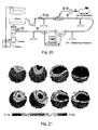
- FIG. 21 is reconstructed 2D images in respect to typical air cavity formation in the flow loop
- FIG. 22 is a sequence of cross section images of a human hand in 5.16 mS/cm brine, which were reconstructed using STM algorithm with three steps of inversion;
- FIG. 23 shows 3-D hand images interpolated from the 2-D EIT images given in FIG. 22 and then iso-surfaced with a cutting value 3.3 mS/cm (Spyglass v1.01).
- the electrically conductive ring sensor basically consists of an electrically conductive ring 1 , a number of electrical contacts 2 , a target content 3 , a number of electrical excitation sources 4 and a number of voltage measurement devices 5 [FIG. 1 ].
- the electrically conductive ring 1 is made of solid substances such as a kind of metals or alternatively, other electrically conductive materials such as conductive rubber or ceramic-metal with a conductivity value much higher than that of the content 3 to be measured.
- the electrically conductive ring acts as an ‘continuous electrode’ to distribute the electrical current flow and generate an electric field for mapping the impedance distribution of the content 3 due to applying currents from the metallic contacts 2 .
- the metallic contacts 2 are embedded into the electrically conductive ring in good electrical contact with the outside wall of the electrically conductive ring.
- the size of these contacts 2 may be very small since a low common voltage on the contacts is produced from the high conductive ring 1 and there is no effects of electrode-electrolyte interface between these contacts 2 and the electrically conductive ring 1 if the ring is made of solid substance. Therefore, the amount of the contacts to be installed could be much more than the number of discrete electrodes in the conventional sensors.
- a number of electrical excitation sources, such as the currents or voltages 4 are applied to one or more electrical contacts 2 . Boundary voltages or currents are also measured from the electrical contacts 2 .
- a continuous electric field distribution presents along the inner surface of the electrically conductive ring that is in electrical contact with the target content 3 .
- the target content 3 may be a process fluid with electrically continuous phase, such as that in a miscible liquid mixing, or with electrically discontinuous phases, such as those in oil-water-gas flow or froth formation [FIG. 2 ]. Since no discrete electrode directly contact to the target content 3 , the excitation and measurement will not get into saturation under a certain current value when apart of the inner sensing surface loses an electrical contact to the principle flow.
- FIG. 3 illustrates its flange configuration.
- FIGS. 4 a and 4 b Comparisons of the potential distributions generated from a sensor with discrete electrodes ( FIGS. 4 a and 4 b ) and the electrically conductive ring sensor ( FIGS. 5 a and 5 b ) are given, which were simulated using Ansoft Maxwell 2D simulator [Version 1-7-66, 1996, Ansoft Corporation]. In the simulation, the conductivity of the electrically conductive ring was ten times as that of the target content.
- the potential distributions in FIGS. 4 a and 5 a were generated from a current excitation between an adjacent electrode/contact pair.
- FIGS. 4 a and 5 a were generated from a current excitation between an adjacent electrode/contact pair.
- FIGS. 4 b and 5 b are potential distributions relating to an opposite electrode/contact pair excitation position.
- the potential distributions in FIGS. 5 a and 5 b are more equal-spaced than those given in FIGS. 4 a and 4 b.
- the field-stream lines can be derived from the equal-potential lines based on the orthogonal method. Therefore, the simulation demonstrates that the electric field intensity distribution generated from the electrically conductive ring sensor are more uniform than that generated from a discrete electrode sensor if the conductivity of the ring 1 is high than the conductivity of the target content 3 .
- FIG. 6 shows the extension for the sensor with discrete electrodes.
- the measurement relationship between one and other sensing strategies for a 4-electrode measurement protocol can be derived as Equation 1 & 2 based on the reciprocity theorem [Geselowitz, IEEE Trans. Biomed Eng. BME-18], which may be summarised as ‘with a 4-electrode measurement protocol, the boundary measurements and the sensitivity matrix for an alternative sensing strategy can be derived from the complete set of independent measurements and the sensitivity matrix obtained from a known sensing strategy’.
- the measurements based on the alternative sensing strategy can not generate any more new information than that given from the complete set of independent measurements, but could produce a different signal-to-noise ratio and a different sensitivity distribution over the imaging domain.
- Equation 1 A general form of the boundary voltage relationship between an alternative 4-electrode sensing strategy and adjacent sensing strategy can be expressed as Equation 1, which derives mutual impedance or boundary voltages for an alternative 4-electrode sensing strategy from those for adjacent electrode pair strategy.
- Z I,J (I M,N ) represents the mutual impedance obtained from voltage measured between electrode I and J when current presents between electrode M and N.
- the sensitivity matrix of an alternative sensing strategy can also be derived from algebraic combination of the sensitivity matrix obtained from a complete set of independent measurements because a linear approximation is adopted in the calculation of the sensitivity matrix, and the linear relationship between the two sets of boundary voltages exist Equation 1). Derivation to a new sensitivity matrix for an alternative strategy from the sensitivity matrix of adjacent electrode pair strategy is given in Equation 2.
- S I,J (I M,N ) represents the sensitivity coefficient at pixel, k, obtained from the measurement and excitation position where the voltage is measured between Electrode I and J when current presents between electrode M and N.
- FIG. 7 shows one of the sensitivity maps relating to the measurement position opposite to the current injection. Summing the coefficients from the seventy-two normalised sensitivity maps at each pixel, it gives an overall sensitivity distribution as FIG. 9 .
- FIG. 9 and FIG. 10 two related sensitivity maps obtained from adjacent sensing strategy are given in FIG. 9 and FIG. 10 . It can be seen that FIG.
- the sensitivity matrix for such specific distribution can be derived from either the alternative sensing strategy or the particulate combination of the sensitivity matrix derived from a known basic set of independent measurements (e.g. adjacent electrode pair sensing strategy).
- the sensor geometry and its conductivity value can be further optimised.
- the ill conditioning of the sensitivity matrix is related to the non-homogeneity of the sensitivity field.
- the smallest sensitivity is related to the central elements with largest related to periphery elements [Yorkey, et al, IEEE Trans. Biomed. Eng., BME 34(11), 1987].
- FIG. 12 shows the sensor geometry used during the optimum design.
- sixteen electrical contacts are distributed around the conductive ring, possessing half of the circumference of the external side of the ring.
- the ring itself has an internal diameter of 5 cm.
- the conductive ring thickness, t was varied during the simulations. The value of t was assumed to be 0.2 cm, 0.6 cm, 0.8 cm, and 1.0 cm.
- the conductivity of the ring is also a variable ranging from 0.11 ms/cm to 0.66 ms/cm.
- the sensor was assumed filled with water with a conductivity of 0.11 ms/cm.
- FIG. 13 A comparison of sensitivity distribution across the diameter is shown in FIG. 13 , where the current is injected from electrode 1 and 2 with measurements taken from electrodes 9 and 10 .
- the distribution in the conductive ring sensor shows more homogenous than that in traditional sensors.
- the important parameters are the ratio of the conductivity and thickness of the ring to those of the material filling the sensor, rather than their absolute values.
- the numerical results for one case could be obtained from another case by appropriate scaling if the same conductivity and thickness ratio were used in simulations.
- a sensitivity matrix for a commonly used adjacent sensing protocol [Brown et al, Proc. IEE Int. Conf. on Electric and Magnetic field in Med. and Bio, 1985] is computed and condition number calculated for each conductivity and thickness value.
- FIG. 14 shows the distribution of the condition number of the sensitivity matrix when the thickness and conductivity of the conductive ring sensor varies.
- the illness measure decreases with the increase of the conductivity and the thickness of the conductive ring sensor, as was confirmed by visualisation with Maxwell 2D simulations.
- the illness measure is not a monotonously decreasing function of the thickness and conductivity of the conductive ring sensor.
- the condition number curve is shown in FIG. 15 . It is found that the illness measure reaches its minimum at the conductivity of 0.66 ms/cm. In FIG. 14 , apparently, the optimal parameters of the conductive ring should be 0.55 ms/cm and 4 mm for the conductivity and the thickness respectively.
- the senor can also be constructed from a conductive disk 11 .
- a hole is drilled in the center of the disk and a layer of metallic coating serving as electrode contacts 2 is made around the ring. [ FIG. 16 a].
- the disk shape sensor can also be configured into a flange or a washer from 18 [ FIG. 16 c].
- PCB 15 can be made to integrate the electrical contacts 2 , wiring 13 and connector 12 [ FIG. 16 b ]. Another advantage of this configuration is its flexibility for replacing the conducive ring once it is contaminated such as in food or pharmaceutical applications.
- the conductive sensor can be made in a micro- or nano-scale using micro-machine technology or integrated circuit fabrication technologies.
- the sensor can also be fabricated integrated with its processing circuits on a single silicon chip.
- Equation 3 The sensitivity theorem deduced by Geselowitz [IEEE Trans. BME-18, 1971] and later refined by Lehr [IEEE Trans. BME-19, 1972] for a two ports system can be expressed in discrete domain as Equation 3 [Murai, et al, IEEE Trans. BME-32, 1985] and Equation 4 [Wang, et al, Chem. Eng. Comm. V175, 1999], assuming the conductivity change is much smaller than the original value ( ⁇ k ⁇ k ) and neglecting the high order terms and supposing that the conductivity distribution is composed from w small uniform ‘patches’ or pixels.
- Equation 5 the sensitivity coefficient, s, for each discrete pixel is given by Equation 5 [Murai, et al, IEEE Trans. BME-32, 1985], where ⁇ k is a discrete area at k.
- ⁇ AB , ⁇ CD are potentials measured from ports A-B and C-D in response to the present of currents I ⁇ and I ⁇ , respectively.
- s jk denotes the sensitivity coefficient at pixel k under the measurement-projection j
- P denotes the maximum number of measurements
- w denotes the maximum number of pixels
- ⁇ k and ⁇ k are the conductivity and conductivity change at pixel k, respectively
- V j and ⁇ V j are in respect to the reference voltage and the voltage change at measurement-projection j.
- Forward solution in the multi-step inverse solution is used for producing an error vector for each step inversion. It also up-dates the sensitivity matrix for next step inverse solution.
- Sensitivity matrix can be derived directly from the nodal voltages obtained from the forward solution [Yorkey, et al, IEEE Trans. BME-34, 1987, Murai, et al, IEEE Trans. BME-32, 1985].
- the actual current value used in the solution is not significant as long as the value doesn't vary in whole process since only relative changes of the boundary voltage measurements are employed in following inverse solution.
- Equation 7 The solution of a FEM model presenting a 2D cross-section of a process vessel with Neumann boundary conditions in addition to a single Dirichlet condition to avoid singularity can be solved by Equation 7 utilising a linear approximation given by Yorkey et al and Murai et al.[Yorkey, et al, IEEE Trans. BME-34, 1987, Murai, et al, IEEE Trans. BME-32, 1985].
- Yv c (7) where Y, v, c denotes the global conductance matrix, the nodal voltage vector, and the nodal current vector respectively.
- the conductivity updating also can be based on an approximation of the inverse relation (Eq.13 based on 1+x ⁇ 1/(1 ⁇ x) at x ⁇ 1), which can improve the convergence speed for both positive and negative changes in conductivity.
- Eq.13 based on 1+x ⁇ 1/(1 ⁇ x) at x ⁇ 1
- step (5) If the convergence or the number of maximum iterations is not reached, the. process jumps to step (5) until one of these conditions is reached. To summarise the procedure, its flowchart is given as FIG. 17 .
- the sensitivity coefficient back-projection approximation method utilising a normalised transpose matrix of the sensitivity matrix obtained from Eq.5 as a weighting matrix, was first refined for ERT by Kotre [Kotre, Physiology Measurements, 15, Suppl. 2A 1992].
- the approximation has been successfully applied to many industrial applications [Williams et al, Process tomography—principles, techniques and applications, Butterworth-Heinemann Ltd., 1995] due to its good anti-noise capability and fast solution speed.
- the physical definition may follow the basic principle of linear back projection: the relative change of the boundary voltage measurements is linearly back-projected to each pixel between two equipotential lines in the case of the equipotential back projection [Baber et al, Applied potential tomography’, J. Phys. E: Sci. Instrum., 17,1984], or over whole domain in the case of the SBP [Kotre, Physiology Measurements, 15, Suppl. 2A 1992].
- the sum of the products of the relative change and the weight factor/sensitivity coefficient at each pixel normalised by the sum of their weight factors/sensitivity coefficients that are derived from all possible boundary measurements, approximately presents the relative change of the conductivity at this pixel.
- FIG. 18 a A set-up with a complex conductivity distribution, as shown in FIG. 18 a, is reconstructed as FIGS. 18 b and 18 c from the SBP and EIDORS algorithms respectively. It is obvious that the SBP algorithm could not deliver an accurate image for this set-up ( FIG. 18 b ). Both the EIDORS ( FIG. 18 c ) and SCG ( FIG. 18 d & f ) can reconstruct the complexity of the set-up. The image obtained from five steps of the SCG solution ( FIG. 18 c ) provides a conductivity error of 3.32% and a boundary voltage error of 0.055%. The discretisation error caused by applying different mesh is reflected in FIG. 3 f.
- FIG. 19 Imaging distinguishability of these algorithms was investigated and the results are given in FIG. 19 .
- Two ‘objects’ were located along a radius of a mesh ( FIG. 19 a ).
- SBP can image the presence of the two objects but could not distinguish them ( FIG. 19 b ).
- the edge of the objects' image is also merged with the boundary.
- the image obtained from EIDORS ( FIG. 19 c ) gives a better presentation about the object location with a clear separation from the boundary but is incapable of distinguishing between the two objects.
- SCG can clearly distinguish between the two objects although a certain artificial background noise presents ( FIG. 19 d & f ).
- the single step method solution is be further simplified by obtaining an approximation of the inverse of ⁇ overscore (s) ⁇ ( ⁇ overscore (s) ⁇ is the normalised sensitivity matrix) and therefore the whole computation for reconstructing a single image only involves a multiplication of a matrix and a vector.
- the detailed information is provided as following.
- ⁇ overscore (s) ⁇ is the normalized sensitivity matrix
- ⁇ the conductivity relative change vector
- e the boundary relative change vector
- equation (16) cannot be solved using direct inverse method aiming to an accurate solution.
- An iterative method with finite steps gives equation (16) an approximation solution, which serves as a kind of regularization.
- iterative methods involves much larger computation load than direct inverse methods by which an inverse matrix for ⁇ overscore (s) ⁇ T ⁇ overscore (s) ⁇ can be obtained, and the solution to equation (16) only involves a multiplication of a matrix ( ⁇ overscore (s) ⁇ T ⁇ overscore (s) ⁇ ) ⁇ 1 ⁇ overscore (s) ⁇ T with an vector e.
- Multiphase flow exists in many industrial processes.
- the phase distribution and interfaces in a multiphase flow carries significant information about the processes [Chhabra et al, Non-newtonian flow in the process industries—fundamentals and engineering applications, Butterworth-Heinemann, Oxford, 1999].
- its behaviour is extremely complex, which presents a great challenge to the study of the flow mechanisms and the measurement of multiphase flow.
- Both single modality and multi-modality imaging have been reported [Dyakowski et al, Powder Technol. 104, 1999; Hoyle et al, Proc. 1st World Congress on Industrial Process Tomography, Buxton, UK, 1999] as a means to identity flow regimes in two-phase flow.
- FIG. 20 A 20 m flow loop (inner diameter, 50 mm) fitted with ERT sensors was employed for the experiments.
- a schematic diagram and overview of the flow loop are given in FIG. 20 .
- the experiments were performed under different air flow-rates of 0.5 m 3 /h, 1.5 m 3 /h, 2.5 m 3 /h, 3.5 m 3 /h and the one less than 0.5 m 3 /h in regard to the productions of slug flow, slug-churn flow, churn flow and bubbly flow regimes.
- the water flows were scaled with an accumulating tank during the experiments to get water flow rate and mean velocity. At the mean time, a number of photographs were recorded as visual presentations of these different flow regimes.
- Two-dimensional (2D) slice images were sequentially reconstructed. Some reconstructed images in respect to typical air cavities in the flow loop are shown in FIG. 21 , where the blue areas represent the air cavities or low conductivity regions and the red areas represent the water or high conductivity regions.
- a human hand was scanned using an EIT system.
- a 14.8 cm diameter vessel fitted with one 16-electrode ring sensor and filled with 5.16 mS/cm brine was employed.
- the adjacent electrode sensing strategy was applied with a pair of 10 mA@9.6 kHz sinusoidal currents for the test.
- the image data was made up of 15 measurement data sets acquired as the hand moved along the axial direction of the phantom while the water volume was kept the same.
- the signal-to-noise-ratio (SNR, here is the repeatability of reference voltage) was checked, which was within a maximum error 0.5%. Fifteen 2D images were reconstructed with the SCG [FIG. 22 ].
Landscapes
- Chemical & Material Sciences (AREA)
- General Health & Medical Sciences (AREA)
- Immunology (AREA)
- Physics & Mathematics (AREA)
- Health & Medical Sciences (AREA)
- Life Sciences & Earth Sciences (AREA)
- Analytical Chemistry (AREA)
- Biochemistry (AREA)
- Chemical Kinetics & Catalysis (AREA)
- Electrochemistry (AREA)
- Pathology (AREA)
- General Physics & Mathematics (AREA)
- Investigating Or Analyzing Materials By The Use Of Electric Means (AREA)
- Medicines Containing Antibodies Or Antigens For Use As Internal Diagnostic Agents (AREA)
- Ultra Sonic Daignosis Equipment (AREA)
- Materials For Medical Uses (AREA)
- Apparatus For Radiation Diagnosis (AREA)
- Analysing Materials By The Use Of Radiation (AREA)
Applications Claiming Priority (5)
| Application Number | Priority Date | Filing Date | Title |
|---|---|---|---|
| GB0031854A GB0031854D0 (en) | 2000-12-30 | 2000-12-30 | Electrical impedance tomography for flow measurement |
| GB0031854.3 | 2000-12-30 | ||
| GB0120772A GB0120772D0 (en) | 2001-08-25 | 2001-08-25 | Electrical impedance tompgraphy for flow measurement |
| GB0120772.9 | 2001-08-25 | ||
| PCT/GB2001/005636 WO2002053029A1 (en) | 2000-12-30 | 2001-12-28 | Electrical impedance tomography |
Publications (2)
| Publication Number | Publication Date |
|---|---|
| US20040130338A1 US20040130338A1 (en) | 2004-07-08 |
| US6940286B2 true US6940286B2 (en) | 2005-09-06 |
Family
ID=26245509
Family Applications (1)
| Application Number | Title | Priority Date | Filing Date |
|---|---|---|---|
| US10/250,327 Expired - Lifetime US6940286B2 (en) | 2000-12-30 | 2001-12-28 | Electrical impedance tomography |
Country Status (6)
| Country | Link |
|---|---|
| US (1) | US6940286B2 (de) |
| EP (1) | EP1347706B1 (de) |
| AT (1) | ATE395866T1 (de) |
| CA (1) | CA2472220A1 (de) |
| DE (1) | DE60134173D1 (de) |
| WO (1) | WO2002053029A1 (de) |
Cited By (52)
| Publication number | Priority date | Publication date | Assignee | Title |
|---|---|---|---|---|
| US20050243087A1 (en) * | 2004-04-30 | 2005-11-03 | Shmuel Aharon | GPU-based Finite Element |
| US20060238194A1 (en) * | 2003-04-15 | 2006-10-26 | Koninklijke Philips Electronics N.V. | Device and method for examination and use of an electrical field in an object under examination containing magnetic particles |
| US20080001608A1 (en) * | 2005-01-05 | 2008-01-03 | Saulnier Gary J | High Precision Voltage Source for Electrical Impedance Tomography |
| CN100362341C (zh) * | 2005-12-22 | 2008-01-16 | 天津大学 | Ert/ect双模态成像系统复合阵列传感器 |
| US20080152203A1 (en) * | 2005-02-03 | 2008-06-26 | Koninklijke Philips Electronics N.V. | Radial Adaptive Filter for Metal Artifact Correction |
| US20090096470A1 (en) * | 2007-10-11 | 2009-04-16 | Rabbitt Richard D | Systems and Methods for Measuring the Electrical Properties of a Microparticle |
| US20090126502A1 (en) * | 2006-05-05 | 2009-05-21 | Arnstein Wee | Method and Apparatus for Tomographic Multiphase Flow Measurements |
| US20100137738A1 (en) * | 2008-10-23 | 2010-06-03 | Robert Beetel | Surgical tissue monitoring system |
| US20110267074A1 (en) * | 2010-04-29 | 2011-11-03 | Schlumberger Technology Corporation | Method of measuring a multiphase flow |
| US8054094B1 (en) | 2010-06-10 | 2011-11-08 | General Electric Company | Image reconstruction based constrained maximization |
| US20130044073A1 (en) * | 2010-05-03 | 2013-02-21 | Flatfrog Laboratories Ab | Touch determination by tomographic reconstruction |
| US8700121B2 (en) | 2011-12-14 | 2014-04-15 | Intersection Medical, Inc. | Devices for determining the relative spatial change in subsurface resistivities across frequencies in tissue |
| US8892379B2 (en) | 2011-06-30 | 2014-11-18 | General Electric Company | System and method for soft-field reconstruction |
| US8963562B2 (en) | 2011-08-31 | 2015-02-24 | General Electric Company | Transducer configurations and methods for transducer positioning in electrical impedance tomography |
| US20150196220A1 (en) * | 2005-09-21 | 2015-07-16 | Beth Israel Deaconess Medical Center, Inc. | Electrical impedance myography |
| WO2016042316A1 (en) * | 2014-09-15 | 2016-03-24 | University Of Leeds | Tomography apparatus and method |
| US9442574B2 (en) | 2008-12-05 | 2016-09-13 | Flatfrog Laboratories Ab | Touch sensing apparatus and method of operating the same |
| US9585593B2 (en) | 2009-11-18 | 2017-03-07 | Chung Shing Fan | Signal distribution for patient-electrode measurements |
| US9615767B2 (en) | 2009-10-26 | 2017-04-11 | Impedimed Limited | Fluid level indicator determination |
| US9724012B2 (en) | 2005-10-11 | 2017-08-08 | Impedimed Limited | Hydration status monitoring |
| US9874978B2 (en) | 2013-07-12 | 2018-01-23 | Flatfrog Laboratories Ab | Partial detect mode |
| US10019113B2 (en) | 2013-04-11 | 2018-07-10 | Flatfrog Laboratories Ab | Tomographic processing for touch detection |
| US10070800B2 (en) | 2007-08-09 | 2018-09-11 | Impedimed Limited | Impedance measurement process |
| US10126882B2 (en) | 2014-01-16 | 2018-11-13 | Flatfrog Laboratories Ab | TIR-based optical touch systems of projection-type |
| US10146376B2 (en) | 2014-01-16 | 2018-12-04 | Flatfrog Laboratories Ab | Light coupling in TIR-based optical touch systems |
| US10161886B2 (en) | 2014-06-27 | 2018-12-25 | Flatfrog Laboratories Ab | Detection of surface contamination |
| US10168835B2 (en) | 2012-05-23 | 2019-01-01 | Flatfrog Laboratories Ab | Spatial resolution in touch displays |
| US10282035B2 (en) | 2016-12-07 | 2019-05-07 | Flatfrog Laboratories Ab | Touch device |
| US10307074B2 (en) | 2007-04-20 | 2019-06-04 | Impedimed Limited | Monitoring system and probe |
| US10318074B2 (en) | 2015-01-30 | 2019-06-11 | Flatfrog Laboratories Ab | Touch-sensing OLED display with tilted emitters |
| US10401546B2 (en) | 2015-03-02 | 2019-09-03 | Flatfrog Laboratories Ab | Optical component for light coupling |
| US10437389B2 (en) | 2017-03-28 | 2019-10-08 | Flatfrog Laboratories Ab | Touch sensing apparatus and method for assembly |
| US10481737B2 (en) | 2017-03-22 | 2019-11-19 | Flatfrog Laboratories Ab | Pen differentiation for touch display |
| US10496227B2 (en) | 2015-02-09 | 2019-12-03 | Flatfrog Laboratories Ab | Optical touch system comprising means for projecting and detecting light beams above and inside a transmissive panel |
| WO2020113157A1 (en) * | 2018-11-28 | 2020-06-04 | Northwestern University | High resolution two-dimensional resistance tomography |
| US10732017B2 (en) | 2014-09-15 | 2020-08-04 | University Of Leeds | Tomography apparatus, multi-phase flow monitoring system, and corresponding methods |
| US10761657B2 (en) | 2016-11-24 | 2020-09-01 | Flatfrog Laboratories Ab | Automatic optimisation of touch signal |
| US10781687B2 (en) | 2015-12-16 | 2020-09-22 | Halliburton Energy Services, Inc. | Electrical impedance tomography using a switchable array |
| US11182023B2 (en) | 2015-01-28 | 2021-11-23 | Flatfrog Laboratories Ab | Dynamic touch quarantine frames |
| US11256371B2 (en) | 2017-09-01 | 2022-02-22 | Flatfrog Laboratories Ab | Optical component |
| US11301089B2 (en) | 2015-12-09 | 2022-04-12 | Flatfrog Laboratories Ab | Stylus identification |
| US11474644B2 (en) | 2017-02-06 | 2022-10-18 | Flatfrog Laboratories Ab | Optical coupling in touch-sensing systems |
| US11536676B2 (en) | 2020-10-02 | 2022-12-27 | Triad National Security, Llc | Characterization of fluid inside pipe using multi frequency electrical signal |
| US11567610B2 (en) | 2018-03-05 | 2023-01-31 | Flatfrog Laboratories Ab | Detection line broadening |
| US20230082500A1 (en) * | 2021-08-26 | 2023-03-16 | Beihang University | Dynamic impedance imaging system |
| US11660013B2 (en) | 2005-07-01 | 2023-05-30 | Impedimed Limited | Monitoring system |
| US11737678B2 (en) | 2005-07-01 | 2023-08-29 | Impedimed Limited | Monitoring system |
| US11893189B2 (en) | 2020-02-10 | 2024-02-06 | Flatfrog Laboratories Ab | Touch-sensing apparatus |
| US11943563B2 (en) | 2019-01-25 | 2024-03-26 | FlatFrog Laboratories, AB | Videoconferencing terminal and method of operating the same |
| US12055969B2 (en) | 2018-10-20 | 2024-08-06 | Flatfrog Laboratories Ab | Frame for a touch-sensitive device and tool therefor |
| US12056316B2 (en) | 2019-11-25 | 2024-08-06 | Flatfrog Laboratories Ab | Touch-sensing apparatus |
| US12282653B2 (en) | 2020-02-08 | 2025-04-22 | Flatfrog Laboratories Ab | Touch apparatus with low latency interactions |
Families Citing this family (30)
| Publication number | Priority date | Publication date | Assignee | Title |
|---|---|---|---|---|
| DE10238824A1 (de) * | 2002-08-23 | 2004-03-11 | Forschungszentrum Jülich GmbH | Verfahren und Vorrichtung zur schnellen tomographischen Messung der elektrischen Leitfähigkeitsverteilung in einer Probe |
| AU2003900857A0 (en) * | 2003-02-26 | 2003-03-13 | Commonwealth Scientific And Industrial Research Organisation | Method and apparatus for characterising multiphase fluid mixtures |
| WO2007088517A2 (en) | 2006-02-01 | 2007-08-09 | Ecole Polytechnique Federale De Lausanne (Epfl) | Apparatus for manipulating, modifying and characterizing particles in a micro channel |
| CN100401044C (zh) * | 2006-03-21 | 2008-07-09 | 天津大学 | 双模电成像系统传感器及基于该传感器的图像重建方法 |
| CN100549684C (zh) * | 2007-04-18 | 2009-10-14 | 天津大学 | 基于方形双模自标定传感器的图像重建方法 |
| FI123318B (fi) * | 2009-09-29 | 2013-02-28 | Outotec Oyj | Massavirtauksen kolmiulotteinen kuvantaminen |
| US8121804B2 (en) * | 2010-01-05 | 2012-02-21 | General Electric Company | Electrical network analysis of a multiphase system |
| US8508238B2 (en) | 2010-08-12 | 2013-08-13 | General Electric Company | System and method for performing electrical impedance tomography |
| FI123789B (fi) | 2010-11-30 | 2013-10-31 | Metso Automation Oy | Suspension kiinteän aineen määrän mittaus |
| CN102274025B (zh) * | 2011-05-30 | 2012-11-28 | 郑州大学 | 多电极电阻抗断层成像数据采集系统 |
| US9989453B2 (en) * | 2011-08-23 | 2018-06-05 | Cidra Corporate Services, Inc. | Tomographic determination of scale build-up in pipes and other tanks, cells, vessels or containers |
| WO2013081845A1 (en) * | 2011-11-30 | 2013-06-06 | General Electric Company | High-side current measurement technique for multi-phase fluid |
| CN103018284B (zh) * | 2012-12-14 | 2015-05-13 | 北京航空航天大学 | 一种基于二端子阻抗测量模式的四端子电阻抗层析成像方法 |
| CN103604993B (zh) * | 2013-09-12 | 2017-01-04 | 陕西航天导航设备有限公司 | 导电装置动态接触电阻测试设备及测试方法 |
| JP6423183B2 (ja) * | 2014-06-25 | 2018-11-14 | 株式会社Ihi | トモグラフィ計測方法 |
| CN105675658A (zh) * | 2016-01-13 | 2016-06-15 | 天津大学 | 具有内置导体环的电阻层析成像传感器 |
| GB2546522B (en) * | 2016-01-21 | 2020-02-12 | Atout Process Ltd | Method and apparatus for measuring flows |
| CN105954351B (zh) * | 2016-04-11 | 2019-03-26 | 中国石油大学(华东) | 基于电磁-声耦合的油水两相流过程层析成像方法 |
| DE102016114611A1 (de) | 2016-08-07 | 2018-02-08 | Karl-Heinz Fromm | Elektrodenanordnung, insbesondere für die Elektrische Impedanz Tomographie |
| DE102016223029A1 (de) | 2016-11-22 | 2018-05-24 | Leibniz-Institut Für Festkörper-Und Werkstoffforschung Dresden E.V. | Dreidimensionaler tomograf |
| KR102241035B1 (ko) * | 2018-11-16 | 2021-04-16 | 경희대학교 산학협력단 | 다채널 배열전극 프로브를 이용한 스크리닝 장치 및 그 동작 방법 |
| EP3698713B1 (de) | 2019-02-20 | 2023-09-06 | Löwenstein Medical Technology S.A. | System zur erfassung von atemanstrengungen eines patienten |
| DE102020100980A1 (de) | 2020-01-16 | 2021-07-22 | Endress+Hauser SE+Co. KG | Verfahren zur Bestimmung und/oder Überwachung zumindest einer Eigenschaft eines Mediums |
| CN113724349B (zh) * | 2021-07-30 | 2025-05-30 | 神华上航疏浚有限责任公司 | 水平管道流速计算方法、装置、计算机设备和存储介质 |
| CN113945609B (zh) * | 2021-10-13 | 2024-03-19 | 中国人民解放军国防科技大学 | 一种用于高铁接触线磨损检测的ert传感器 |
| CN114062435A (zh) * | 2021-10-21 | 2022-02-18 | 北京工业大学 | 基于电阻抗成像原理的具有灵敏度修正功能的柔性传感器 |
| CN114216933B (zh) * | 2021-12-16 | 2023-11-24 | 北京航空航天大学 | 一种适用于开域流场的气液两相流测量装置及方法 |
| KR20240083312A (ko) * | 2022-12-05 | 2024-06-12 | 현대자동차주식회사 | 건식 전극 혼합물의 진단시스템 |
| CN116400150A (zh) * | 2023-03-13 | 2023-07-07 | 中国海洋石油集团有限公司 | 一种非接触式饱和场测量系统 |
| FR3152593B1 (fr) * | 2023-09-06 | 2025-09-26 | Commissariat Energie Atomique | Système de réduction ou d’optimisation de la consommation ou de la production électrique d’un équipement fluidique à au moins un composant rotatif. |
Citations (9)
| Publication number | Priority date | Publication date | Assignee | Title |
|---|---|---|---|---|
| GB2019579A (en) | 1978-03-25 | 1979-10-31 | Philips Nv | Method of and a device for determining the internal structure of a body for example a human body |
| GB2119520A (en) | 1982-04-30 | 1983-11-16 | Brian Hilton Brown | Tomography |
| US4486835A (en) | 1981-05-13 | 1984-12-04 | Yeda Research And Development Co. Ltd. | Apparatus and techniques for electric tomography |
| GB2160323A (en) | 1984-06-14 | 1985-12-18 | Univ Sheffield | Tomography |
| US4617939A (en) | 1982-04-30 | 1986-10-21 | The University Of Sheffield | Tomography |
| US4920490A (en) | 1988-01-28 | 1990-04-24 | Rensselaer Polytechnic Institute | Process and apparatus for distinguishing conductivities by electric current computed tomography |
| US5272624A (en) | 1990-10-02 | 1993-12-21 | Rensselaer Polytechnic Institute | Current patterns for impedance tomography |
| WO1995024155A1 (en) | 1994-03-11 | 1995-09-14 | British Technology Group Limited | Electrical impedance tomography |
| WO1998023204A1 (en) | 1996-11-26 | 1998-06-04 | Computing Devices Canada Ltd. | Electrical impedance tomography method and electrode arrangement for use therein |
-
2001
- 2001-12-28 EP EP01272705A patent/EP1347706B1/de not_active Expired - Lifetime
- 2001-12-28 WO PCT/GB2001/005636 patent/WO2002053029A1/en not_active Ceased
- 2001-12-28 CA CA002472220A patent/CA2472220A1/en not_active Abandoned
- 2001-12-28 DE DE60134173T patent/DE60134173D1/de not_active Expired - Lifetime
- 2001-12-28 US US10/250,327 patent/US6940286B2/en not_active Expired - Lifetime
- 2001-12-28 AT AT01272705T patent/ATE395866T1/de not_active IP Right Cessation
Patent Citations (10)
| Publication number | Priority date | Publication date | Assignee | Title |
|---|---|---|---|---|
| GB2019579A (en) | 1978-03-25 | 1979-10-31 | Philips Nv | Method of and a device for determining the internal structure of a body for example a human body |
| US4486835A (en) | 1981-05-13 | 1984-12-04 | Yeda Research And Development Co. Ltd. | Apparatus and techniques for electric tomography |
| GB2119520A (en) | 1982-04-30 | 1983-11-16 | Brian Hilton Brown | Tomography |
| US4617939A (en) | 1982-04-30 | 1986-10-21 | The University Of Sheffield | Tomography |
| GB2160323A (en) | 1984-06-14 | 1985-12-18 | Univ Sheffield | Tomography |
| US4920490A (en) | 1988-01-28 | 1990-04-24 | Rensselaer Polytechnic Institute | Process and apparatus for distinguishing conductivities by electric current computed tomography |
| US5272624A (en) | 1990-10-02 | 1993-12-21 | Rensselaer Polytechnic Institute | Current patterns for impedance tomography |
| WO1995024155A1 (en) | 1994-03-11 | 1995-09-14 | British Technology Group Limited | Electrical impedance tomography |
| WO1998023204A1 (en) | 1996-11-26 | 1998-06-04 | Computing Devices Canada Ltd. | Electrical impedance tomography method and electrode arrangement for use therein |
| US6501984B1 (en) * | 1996-11-26 | 2002-12-31 | Computing Devices Canada Ltd. | Electrical impedance tomography method and electrode arrangement for use therein |
Non-Patent Citations (18)
| Title |
|---|
| Barber et al. "Applied potential tomography," J. Phys. E: Sci. Instrum., vol. 17, 1984, pp. 723-33. No month avail. |
| Brown et al. "Applied Potential Tomography -Data Collection Problems," International Conference on Electric and Magnetic Fields in Medicine and Biology, Dec. 4-5, 1985. |
| Dickin et al. "Electrical resistance tomography for process applications," Measurement Science and Technology, vol. 7, No. 3, Mar. 1, 1996, pp. 247-260. |
| Dyakowski et al. "On-line monitoring of dense phase flow using real time dielectric imaging," Powder Technology, vol. 104, 1999, pp. 287-95. No month available. |
| Geselowitz, David B. "An Application of Electrocardiographic Lead Theory to Impedance Plethysmography," IEEE Transcations on Biomedical Engineering, vol. BME-18, No. 1, Jan. 1971. |
| Hoyle et al. "Multi-Sensor Process Tomography System Design: Part 1 -Systems and Hardware Engineering," 1<SUP>st </SUP>World Congress on Industrial Process Tomography, Buxton, Greater Manchester, Apr. 14-17, 1999. |
| International Search Report dated Mar. 25, 2002 for PCT/GB01/05636. |
| Kotre, C.J. "EIT image reconstruction using sensitivity weighted filtered backprojection," Phsiol. Meas. vol. 15, 1994, pp. A125-A136. No month available. |
| Lehr, John, "Short Communications: A Vector Derivation Useful in Impedance Plethysmographic Field Calculations," IEEE Transactions on Biomedical Engineering, vol. BME-19, Mar. 1972. |
| Lucas et al. "Measurement of the solids volume fraction and velocity distributions in solids -liquid flows using dual-plane electrical resistance tomography," Journal of Flow Measurement and Instrumentation, Oct. 4, 1999. No month available. |
| Lucas et al. "Measurement of the solids volume fraction and velocity distributions in solids-liquid flows using dual plane electrical resistance tomography," Flow Measurement and Instrumentation, vol. 10, 1999, pp. 249-58. No month. |
| Murai et al. "Electrical Impedance Computed Tomography Based on a Finite Element Model," IEEE Transactions on Biomedical Engineering, vol. BME-32, No. 3, Mar. 1985. |
| Seleghim et al. "Direct imaging of two-phase flows by electrical impedance measurements," Measurement Science and Technology, vol. 9, No. 9, Sep. 1998, pp. 1492-1500. |
| Tai et al. "An experimental electrical impedance tomography system," Proceedings of the Region Ten Conference, Beijing, Oct. 19-21, 1993, vol. 3. |
| Wang et al. "Detecting non-uniform foam density using electrical resistance tomography," Chemical Engineering Science, vol. 54, 1999, pp. 707-12. No month available. |
| Wang et al. "Electrical Resistance Tomographic Sensing Systems for Industrial Applications," Chem. Eng. Comm., 1999, vol. 175, pp. 49-70. No month available. |
| Wang et al. "Modelling and analysis of electrically conducting vessels and pipelines in electrical resistance process tomography," IEE Proc.-Sci. Meas. Technol., vol. 412, No. 4, Jul. 1995. |
| Yorkey et al. "Comparing Reconstruction Algorithms for Electrical Impedance Tomography," IEEE Transactions on Biomedical Engineering, vol. BME-34, No. 11, Nov. 1987. |
Cited By (93)
| Publication number | Priority date | Publication date | Assignee | Title |
|---|---|---|---|---|
| US20060238194A1 (en) * | 2003-04-15 | 2006-10-26 | Koninklijke Philips Electronics N.V. | Device and method for examination and use of an electrical field in an object under examination containing magnetic particles |
| US11045107B2 (en) | 2003-04-15 | 2021-06-29 | Koninklijke Philips N.V. | Device and method for examination and use of an electrical field in an object under examination containing magnetic particles |
| US8532735B2 (en) * | 2003-04-15 | 2013-09-10 | Koninklijke Philips N.V. | Device and method for examination and use of an electrical field in an object under examination containing magnetic particles |
| US20050243087A1 (en) * | 2004-04-30 | 2005-11-03 | Shmuel Aharon | GPU-based Finite Element |
| US20080001608A1 (en) * | 2005-01-05 | 2008-01-03 | Saulnier Gary J | High Precision Voltage Source for Electrical Impedance Tomography |
| US7701227B2 (en) * | 2005-01-05 | 2010-04-20 | Rensselaer Polytechnic Institute | High precision voltage source for electrical impedance tomography |
| US7991243B2 (en) * | 2005-02-03 | 2011-08-02 | Koninklijke Philips Electronics N.V. | Radial adaptive filter for metal artifact correction |
| US20080152203A1 (en) * | 2005-02-03 | 2008-06-26 | Koninklijke Philips Electronics N.V. | Radial Adaptive Filter for Metal Artifact Correction |
| US11737678B2 (en) | 2005-07-01 | 2023-08-29 | Impedimed Limited | Monitoring system |
| US11660013B2 (en) | 2005-07-01 | 2023-05-30 | Impedimed Limited | Monitoring system |
| US20150196220A1 (en) * | 2005-09-21 | 2015-07-16 | Beth Israel Deaconess Medical Center, Inc. | Electrical impedance myography |
| US10898100B2 (en) * | 2005-09-21 | 2021-01-26 | Beth Israel Deaconess Medical Center, Inc. | Electrical impedance myography |
| US9724012B2 (en) | 2005-10-11 | 2017-08-08 | Impedimed Limited | Hydration status monitoring |
| US11612332B2 (en) | 2005-10-11 | 2023-03-28 | Impedimed Limited | Hydration status monitoring |
| CN100362341C (zh) * | 2005-12-22 | 2008-01-16 | 天津大学 | Ert/ect双模态成像系统复合阵列传感器 |
| US7624652B2 (en) | 2006-05-05 | 2009-12-01 | Multi Phase Meters As | Method and apparatus for tomographic multiphase flow measurements |
| US20090126502A1 (en) * | 2006-05-05 | 2009-05-21 | Arnstein Wee | Method and Apparatus for Tomographic Multiphase Flow Measurements |
| US10307074B2 (en) | 2007-04-20 | 2019-06-04 | Impedimed Limited | Monitoring system and probe |
| US10070800B2 (en) | 2007-08-09 | 2018-09-11 | Impedimed Limited | Impedance measurement process |
| US8102182B2 (en) | 2007-10-11 | 2012-01-24 | University Of Utah Research Foundation | Systems and methods for measuring the electrical properties of a microparticle |
| US20090096470A1 (en) * | 2007-10-11 | 2009-04-16 | Rabbitt Richard D | Systems and Methods for Measuring the Electrical Properties of a Microparticle |
| US8386010B2 (en) | 2008-10-23 | 2013-02-26 | Covidien Lp | Surgical tissue monitoring system |
| US20100137738A1 (en) * | 2008-10-23 | 2010-06-03 | Robert Beetel | Surgical tissue monitoring system |
| US10474249B2 (en) | 2008-12-05 | 2019-11-12 | Flatfrog Laboratories Ab | Touch sensing apparatus and method of operating the same |
| US10048773B2 (en) | 2008-12-05 | 2018-08-14 | Flatfrog Laboratories Ab | Touch sensing apparatus and method of operating the same |
| US9442574B2 (en) | 2008-12-05 | 2016-09-13 | Flatfrog Laboratories Ab | Touch sensing apparatus and method of operating the same |
| US9615767B2 (en) | 2009-10-26 | 2017-04-11 | Impedimed Limited | Fluid level indicator determination |
| US9585593B2 (en) | 2009-11-18 | 2017-03-07 | Chung Shing Fan | Signal distribution for patient-electrode measurements |
| US9645130B2 (en) | 2010-04-29 | 2017-05-09 | Schlumberger Technology Corporation | Measuring properties of a multiphase mixture flow |
| US20110267074A1 (en) * | 2010-04-29 | 2011-11-03 | Schlumberger Technology Corporation | Method of measuring a multiphase flow |
| US8536883B2 (en) * | 2010-04-29 | 2013-09-17 | Schlumberger Technology Corporation | Method of measuring a multiphase flow |
| US9547393B2 (en) | 2010-05-03 | 2017-01-17 | Flatfrog Laboratories Ab | Touch determination by tomographic reconstruction |
| US8780066B2 (en) * | 2010-05-03 | 2014-07-15 | Flatfrog Laboratories Ab | Touch determination by tomographic reconstruction |
| US9996196B2 (en) | 2010-05-03 | 2018-06-12 | Flatfrog Laboratories Ab | Touch determination by tomographic reconstruction |
| US20130044073A1 (en) * | 2010-05-03 | 2013-02-21 | Flatfrog Laboratories Ab | Touch determination by tomographic reconstruction |
| US8054094B1 (en) | 2010-06-10 | 2011-11-08 | General Electric Company | Image reconstruction based constrained maximization |
| US8892379B2 (en) | 2011-06-30 | 2014-11-18 | General Electric Company | System and method for soft-field reconstruction |
| US8963562B2 (en) | 2011-08-31 | 2015-02-24 | General Electric Company | Transducer configurations and methods for transducer positioning in electrical impedance tomography |
| US9149225B2 (en) | 2011-12-14 | 2015-10-06 | Intesection Medical, Inc. | Methods for determining the relative spatial change in subsurface resistivities across frequencies in tissue |
| US8700121B2 (en) | 2011-12-14 | 2014-04-15 | Intersection Medical, Inc. | Devices for determining the relative spatial change in subsurface resistivities across frequencies in tissue |
| US10168835B2 (en) | 2012-05-23 | 2019-01-01 | Flatfrog Laboratories Ab | Spatial resolution in touch displays |
| US10019113B2 (en) | 2013-04-11 | 2018-07-10 | Flatfrog Laboratories Ab | Tomographic processing for touch detection |
| US9874978B2 (en) | 2013-07-12 | 2018-01-23 | Flatfrog Laboratories Ab | Partial detect mode |
| US10126882B2 (en) | 2014-01-16 | 2018-11-13 | Flatfrog Laboratories Ab | TIR-based optical touch systems of projection-type |
| US10146376B2 (en) | 2014-01-16 | 2018-12-04 | Flatfrog Laboratories Ab | Light coupling in TIR-based optical touch systems |
| US10161886B2 (en) | 2014-06-27 | 2018-12-25 | Flatfrog Laboratories Ab | Detection of surface contamination |
| US10371656B2 (en) | 2014-09-15 | 2019-08-06 | University Of Leeds | Tomography apparatus and method |
| WO2016042316A1 (en) * | 2014-09-15 | 2016-03-24 | University Of Leeds | Tomography apparatus and method |
| US10732017B2 (en) | 2014-09-15 | 2020-08-04 | University Of Leeds | Tomography apparatus, multi-phase flow monitoring system, and corresponding methods |
| US11182023B2 (en) | 2015-01-28 | 2021-11-23 | Flatfrog Laboratories Ab | Dynamic touch quarantine frames |
| US10318074B2 (en) | 2015-01-30 | 2019-06-11 | Flatfrog Laboratories Ab | Touch-sensing OLED display with tilted emitters |
| US11029783B2 (en) | 2015-02-09 | 2021-06-08 | Flatfrog Laboratories Ab | Optical touch system comprising means for projecting and detecting light beams above and inside a transmissive panel |
| US10496227B2 (en) | 2015-02-09 | 2019-12-03 | Flatfrog Laboratories Ab | Optical touch system comprising means for projecting and detecting light beams above and inside a transmissive panel |
| US10401546B2 (en) | 2015-03-02 | 2019-09-03 | Flatfrog Laboratories Ab | Optical component for light coupling |
| US11301089B2 (en) | 2015-12-09 | 2022-04-12 | Flatfrog Laboratories Ab | Stylus identification |
| US10781687B2 (en) | 2015-12-16 | 2020-09-22 | Halliburton Energy Services, Inc. | Electrical impedance tomography using a switchable array |
| US10761657B2 (en) | 2016-11-24 | 2020-09-01 | Flatfrog Laboratories Ab | Automatic optimisation of touch signal |
| US12566525B2 (en) | 2016-12-07 | 2026-03-03 | Flatfrog Laboratories Ab | Touch device |
| US10775935B2 (en) | 2016-12-07 | 2020-09-15 | Flatfrog Laboratories Ab | Touch device |
| US11579731B2 (en) | 2016-12-07 | 2023-02-14 | Flatfrog Laboratories Ab | Touch device |
| US12189906B2 (en) | 2016-12-07 | 2025-01-07 | Flatfrog Laboratories Ab | Touch device |
| US10282035B2 (en) | 2016-12-07 | 2019-05-07 | Flatfrog Laboratories Ab | Touch device |
| US11281335B2 (en) | 2016-12-07 | 2022-03-22 | Flatfrog Laboratories Ab | Touch device |
| US11474644B2 (en) | 2017-02-06 | 2022-10-18 | Flatfrog Laboratories Ab | Optical coupling in touch-sensing systems |
| US12524117B2 (en) | 2017-02-06 | 2026-01-13 | Flatfrog Laboratories Ab | Optical coupling in touch-sensing systems |
| US12175044B2 (en) | 2017-02-06 | 2024-12-24 | Flatfrog Laboratories Ab | Optical coupling in touch-sensing systems |
| US11740741B2 (en) | 2017-02-06 | 2023-08-29 | Flatfrog Laboratories Ab | Optical coupling in touch-sensing systems |
| US10606414B2 (en) | 2017-03-22 | 2020-03-31 | Flatfrog Laboratories Ab | Eraser for touch displays |
| US11099688B2 (en) | 2017-03-22 | 2021-08-24 | Flatfrog Laboratories Ab | Eraser for touch displays |
| US10481737B2 (en) | 2017-03-22 | 2019-11-19 | Flatfrog Laboratories Ab | Pen differentiation for touch display |
| US11016605B2 (en) | 2017-03-22 | 2021-05-25 | Flatfrog Laboratories Ab | Pen differentiation for touch displays |
| US10606416B2 (en) | 2017-03-28 | 2020-03-31 | Flatfrog Laboratories Ab | Touch sensing apparatus and method for assembly |
| US10437389B2 (en) | 2017-03-28 | 2019-10-08 | Flatfrog Laboratories Ab | Touch sensing apparatus and method for assembly |
| US10739916B2 (en) | 2017-03-28 | 2020-08-11 | Flatfrog Laboratories Ab | Touch sensing apparatus and method for assembly |
| US11281338B2 (en) | 2017-03-28 | 2022-03-22 | Flatfrog Laboratories Ab | Touch sensing apparatus and method for assembly |
| US10845923B2 (en) | 2017-03-28 | 2020-11-24 | Flatfrog Laboratories Ab | Touch sensing apparatus and method for assembly |
| US11269460B2 (en) | 2017-03-28 | 2022-03-08 | Flatfrog Laboratories Ab | Touch sensing apparatus and method for assembly |
| US12086362B2 (en) | 2017-09-01 | 2024-09-10 | Flatfrog Laboratories Ab | Optical component |
| US11650699B2 (en) | 2017-09-01 | 2023-05-16 | Flatfrog Laboratories Ab | Optical component |
| US11256371B2 (en) | 2017-09-01 | 2022-02-22 | Flatfrog Laboratories Ab | Optical component |
| US11567610B2 (en) | 2018-03-05 | 2023-01-31 | Flatfrog Laboratories Ab | Detection line broadening |
| US12524116B2 (en) | 2018-03-05 | 2026-01-13 | Flatfrog Laboratories Ab | Detection line broadening |
| US12055969B2 (en) | 2018-10-20 | 2024-08-06 | Flatfrog Laboratories Ab | Frame for a touch-sensitive device and tool therefor |
| US12357188B2 (en) | 2018-11-28 | 2025-07-15 | Northwestern University | High resolution two-dimensional resistance tomography |
| WO2020113157A1 (en) * | 2018-11-28 | 2020-06-04 | Northwestern University | High resolution two-dimensional resistance tomography |
| US11943563B2 (en) | 2019-01-25 | 2024-03-26 | FlatFrog Laboratories, AB | Videoconferencing terminal and method of operating the same |
| US12056316B2 (en) | 2019-11-25 | 2024-08-06 | Flatfrog Laboratories Ab | Touch-sensing apparatus |
| US12461630B2 (en) | 2019-11-25 | 2025-11-04 | Flatfrog Laboratories Ab | Touch-sensing apparatus |
| US12282653B2 (en) | 2020-02-08 | 2025-04-22 | Flatfrog Laboratories Ab | Touch apparatus with low latency interactions |
| US11893189B2 (en) | 2020-02-10 | 2024-02-06 | Flatfrog Laboratories Ab | Touch-sensing apparatus |
| US11536676B2 (en) | 2020-10-02 | 2022-12-27 | Triad National Security, Llc | Characterization of fluid inside pipe using multi frequency electrical signal |
| US11754520B2 (en) * | 2021-08-26 | 2023-09-12 | Beihang University | Dynamic impedance imaging system |
| US20230082500A1 (en) * | 2021-08-26 | 2023-03-16 | Beihang University | Dynamic impedance imaging system |
Also Published As
| Publication number | Publication date |
|---|---|
| DE60134173D1 (de) | 2008-07-03 |
| EP1347706A1 (de) | 2003-10-01 |
| ATE395866T1 (de) | 2008-06-15 |
| WO2002053029A1 (en) | 2002-07-11 |
| US20040130338A1 (en) | 2004-07-08 |
| CA2472220A1 (en) | 2002-07-11 |
| EP1347706B1 (de) | 2008-05-21 |
Similar Documents
| Publication | Publication Date | Title |
|---|---|---|
| US6940286B2 (en) | Electrical impedance tomography | |
| Borsic | Regularisation methods for imaging from electrical measurements | |
| EP2483672B1 (de) | Dreidimensionale abbildung eines massenflusses | |
| Ceccio et al. | A review of electrical impedance techniques for the measurement of multiphase flows | |
| Mueller et al. | A direct reconstruction algorithm for electrical impedance tomography | |
| US8614707B2 (en) | 3D and real time electrical capacitance volume-tomography sensor design and image reconstruction | |
| Wang | Inverse solutions for electrical impedance tomography based on conjugate gradients methods | |
| Adler et al. | Electrical impedance tomography | |
| Wang et al. | Electrical resistance tomographic sensing systems for industrial applications | |
| CN109690260B (zh) | 用于有损介质成像的位移电流相位层析成像 | |
| Heikkinen et al. | Real time three-dimensional electrical impedance tomography applied in multiphase flow imaging | |
| Ge et al. | Electromagnetic tomography for multiphase flow in the downhole annulus | |
| CN101794453B (zh) | 基于回归分析的节点映射图像重构方法 | |
| Wang et al. | A highly adaptive electrical impedance sensing system for flow measurement | |
| Liu et al. | A bilateral constrained image reconstruction method using electrical impedance tomography and ultrasonic measurement | |
| Tan et al. | Combinational multimodality tomography system for industrial multiphase flow imaging | |
| Dimas et al. | An efficient point-matching method-of-moments for 2D and 3D electrical impedance tomography using radial basis functions | |
| Arif et al. | Joint reconstruction of conductivity and velocity in two-phase flows using electromagnetic flow tomography and electrical tomography: A simulation study | |
| CN102540276B (zh) | 软场层析成像系统和方法 | |
| Marashdeh | Advances in electrical capacitance tomography | |
| Kwon et al. | Estimation of anomaly location and size using electrical impedance tomography | |
| Heikkinen et al. | Modelling of internal structures and electrodes in electrical process tomography | |
| Babaeizadeh et al. | Electrical impedance tomography for piecewise constant domains using boundary element shape-based inverse solutions | |
| Murphy et al. | Electrical impedance tomography with non-stationary electrodes | |
| Abdullah | Electrical impedance tomography for imaging conducting mixtures in hydrocyclone separators |
Legal Events
| Date | Code | Title | Description |
|---|---|---|---|
| AS | Assignment |
Owner name: LEEDS, THE UNIVERSITY OF, GREAT BRITAIN Free format text: ASSIGNMENT OF ASSIGNORS INTEREST;ASSIGNORS:WANG, MI;YIN, WULIANG;REEL/FRAME:014985/0789;SIGNING DATES FROM 20031219 TO 20031222 |
|
| STCF | Information on status: patent grant |
Free format text: PATENTED CASE |
|
| CC | Certificate of correction | ||
| FEPP | Fee payment procedure |
Free format text: PAYOR NUMBER ASSIGNED (ORIGINAL EVENT CODE: ASPN); ENTITY STATUS OF PATENT OWNER: SMALL ENTITY |
|
| FPAY | Fee payment |
Year of fee payment: 4 |
|
| FPAY | Fee payment |
Year of fee payment: 8 |
|
| FEPP | Fee payment procedure |
Free format text: PAT HOLDER CLAIMS SMALL ENTITY STATUS, ENTITY STATUS SET TO SMALL (ORIGINAL EVENT CODE: LTOS); ENTITY STATUS OF PATENT OWNER: SMALL ENTITY |
|
| FPAY | Fee payment |
Year of fee payment: 12 |