US6898703B1 - System and method for creating a boot file utilizing a boot template - Google Patents
System and method for creating a boot file utilizing a boot template Download PDFInfo
- Publication number
- US6898703B1 US6898703B1 US09/989,819 US98981901A US6898703B1 US 6898703 B1 US6898703 B1 US 6898703B1 US 98981901 A US98981901 A US 98981901A US 6898703 B1 US6898703 B1 US 6898703B1
- Authority
- US
- United States
- Prior art keywords
- boot
- boot file
- present
- configuration
- generation method
- Prior art date
- Legal status (The legal status is an assumption and is not a legal conclusion. Google has not performed a legal analysis and makes no representation as to the accuracy of the status listed.)
- Expired - Lifetime, expires
Links
Images


Classifications
-
- G—PHYSICS
- G06—COMPUTING; CALCULATING OR COUNTING
- G06F—ELECTRIC DIGITAL DATA PROCESSING
- G06F8/00—Arrangements for software engineering
- G06F8/40—Transformation of program code
- G06F8/41—Compilation
- G06F8/44—Encoding
- G06F8/447—Target code generation
-
- G—PHYSICS
- G06—COMPUTING; CALCULATING OR COUNTING
- G06F—ELECTRIC DIGITAL DATA PROCESSING
- G06F9/00—Arrangements for program control, e.g. control units
- G06F9/06—Arrangements for program control, e.g. control units using stored programs, i.e. using an internal store of processing equipment to receive or retain programs
- G06F9/44—Arrangements for executing specific programs
- G06F9/4401—Bootstrapping
Definitions
- Embodiments of the present invention generally relate to the field of integrated circuit chips. More specifically, embodiments of the present invention pertain to a system and method for computer aided design for single-chip microelectronic systems.
- Electronic systems and circuits have made a significant contribution towards the advancement of modern society and are utilized in a number of applications to achieve advantageous results.
- Numerous electronic technologies such as digital computers, calculators, audio devices, video equipment, and telephone systems have facilitated increased productivity and reduced costs in analyzing and communicating data, ideas and trends in most areas of business, science, education and entertainment.
- Electronic systems designed to provide these benefits often include integrated circuits on a single substrate that provide a variety advantages (e.g., such as miniaturization, fast processing of signals, minimal power consumption, etc.) over discrete component circuits.
- advantages e.g., such as miniaturization, fast processing of signals, minimal power consumption, etc.
- traditional approaches to manufacturing and designing single-chip systems are often very complex and consume significant resources.
- Microcontrollers are one example of integrated circuit components with characteristics that are potentially useful in a variety of applications. For example, microcontrollers are typically reliable and relatively economical to produce. Microcontrollers have evolved since they were first introduced and have substantially replaced mechanical and electromechanical components in numerous applications and devices. However, while traditional mircontrollers have some characteristics that are advantageous they also tend to be limited in the number of applications in which any given microcontroller can be utilized.
- each microcontroller was custom designed precisely for a narrow range of applications with a fixed combination of required peripheral functionalities.
- Developing custom microcontroller designs with particular fixed peripherals is time and resource intensive, typically requiring separate and dedicated manufacturing operations for each different microcontroller (which is particularly expensive for small volume batches).
- Even if a microcontroller may suffice for more than one application it is still difficult to select an appropriate microcontroller for a particular application. Determining which one of the different available particular microcontroller designs is best suited for a particular application is challenging.
- the unique aspects of the intended application often make it difficult to find an optimum microcontroller, usually necessitating a compromise between the convenience of using an existing microcontroller design and less than optimum performance. Even when a suitable microcontroller is found, subsequent changes to the application and new requirements placed on the application can lead to the need for a totally different microcontroller.
- ASICs Application specific integrated circuits
- ASICs may appear to address some of the issues associated with finding a suitable microcontroller for a particular application, but they tend to present significant hurdles.
- ASICs can be problematic because they tend to require a sophisticated amount of design expertise and the obstacles of long development times, high costs, and large volume requirements still remain.
- Prior attempts at providing limited flexibility by the use of gate arrays and or other logic components are very expensive and require a sophisticated level of design expertise. Even after determining what functions and configurations is desirable, additional significant resources are necessary in systems requiring software code for the performance of appropriate functions.
- Numerous electronic devices require some type of boot sequence to begin operations.
- Some traditional integrated circuit designs required the generation of programmed boot code that directs the sequence of boot operations performed by components included in the integrated circuit.
- the programmed boot code is manually written by an application programmer, requiring the programmer to have knowledge of all the components and the numerous logical values (such as a bit stream) that direct a component to perform desired functions.
- different boot configurations and functions typically result in interrupts to different vectors and tracking the corresponding interrupt vector is very difficult and often susceptible to erroneous coding.
- the present invention is a system and method of facilitating automatic generation of the boot sequence instructions in a convenient and efficient manner.
- an electronic device boot file generation method is utilized to create a boot file.
- a boot template file is created comprising special symbolic variable names that point to configuration registers within an electronic device.
- the electronic device is a programmable device.
- User module selections are received with delineations of preferred configurations and functions associated with components of the programmable device.
- Application files are automatically generated based upon user module selections of configurations and functions utilizing the symbolic variable register names. Subsequent to user module selections, special symbolic variable register names are substituted or replaced with actual configuration register names.
- a present invention programmable device boot file generation method also facilitates providing the appropriate interrupt vectors to their respective interrupt processing routines.
- an electronic device boot file generation method is performed by the electronic device's software design tool.
- the tool provides an interface for selecting applicable user modules, facilitates programming of desired functionality into the target device; and executes an assembler process.
- the tool produces a configuration image that defines configurations and functionalities of the electronic device and are stored in a memory included in the electronic device.
- the configuration image data may be generated and loaded on the electronic device in various manners including by one embodiment of a present invention.
- a software design tool comprising an editor for defining user module personalization and parameterization, an application editor for editing and compiling automatically generated and user created application program interface (API) code, and a debugger assisting debugging operations through emulation of the target device.
- API application program interface
- FIG. 1 is a block diagram showing a high level view of an exemplary integrated circuit (e.g., a microcontroller) upon which embodiments of the present invention may be implemented.
- a microcontroller e.g., a microcontroller
- FIG. 2A is a block diagram of one embodiment of a functional component depicted in greater detail.
- FIG. 2B is a block diagram of one embodiment of a functional block, included in an exemplary implementation of the present invention.
- FIG. 3A is a flow chart of one embodiment of a present invention boot file creation method.
- FIG. 3B is a table illustrating one embodiment of an interrupt vector mapping table of the present invention.
- FIG. 4 is a flow chart of a design tool process illustrating exemplary steps used by a design tool in accordance with one embodiment of the present invention.
- FIG. 5 is a flow chart of one embodiment of a present invention boot sequence.
- FIG. 1 is a block diagram showing a high level view of an exemplary integrated circuit (e.g., a microcontroller) 10 upon which embodiments of the present invention may be implemented.
- integrated circuit 10 includes a communication bus 11 , static random access memory (SRAM) 12 , central processing unit (CPU) 14 , flash read-only memory (ROM) 15 , input/output (I/O) pin(s) 18 and functional component 25 .
- Communication bus 11 is electrically coupled to static random access memory (SRAM) 12 , central processing unit (CPU) 14 , flash read-only memory (ROM) 15 , input/output (I/O) pin(s) 18 and functional component 25 .
- Static random access memory (SRAM) 12 stores volatile or temporary data during firmware execution.
- Central processing unit (CPU) 14 processes information and instructions.
- Flash read-only memory (ROM) 15 stores information and instructions (e.g., firmware). In one embodiment of the present invention, flash read-only memory (ROM) 15 stores configuration image data.
- Input/output (I/O) pin(s) 18 provides an interface with external devices (not shown).
- Functional component 25 is programmable to provide different functions and configurations.
- integrated circuit 10 is readily adaptable to include a variety of other components.
- integrated circuit 10 also includes a dedicated functionality internal peripheral component 17 which is coupled to system bus 11 in addition to the functional component 25 .
- An optional test interface (TI) may be coupled to integrated circuit 10 via a test interface coupler (TIC), which may be detachable, to perform debugging operations during startup and initialization of the integrated circuit.
- TI test interface
- TIC test interface coupler
- additional functions such as clocking and power control are provided by a variety of components including a precision oscillator and phase locked loop (PLL), a voltage reference, a 32 kHz crystal oscillator (which may be utilized for a variety of applications such as calibration and synchronization, etc.), an interrupt controller (for generating interrupt signals as required), a power on reset control unit (for performing functions related to power supply stability), and a brown-out detection unit (which detects substandard, subnominal power system parameters).
- PLL precision oscillator and phase locked loop
- VPLL phase locked loop
- a voltage reference which may be utilized for a variety of applications such as calibration and synchronization, etc.
- an interrupt controller for generating interrupt signals as required
- a power on reset control unit for performing functions related to power supply stability
- a brown-out detection unit which detects substandard, subnominal power system parameters.
- functional component 25 includes an analog functional block 230 , a digital functional block 240 , and a programmable interconnect 250 .
- analog functional block 230 includes a matrix of interconnected analog functional blocks A 1 through AN.
- the number N may be any number of analog functional blocks.
- digital block 240 includes a matrix of interconnected digital functional blocks D 1 through DM.
- the number M may be any number of digital functional blocks.
- the analog functional blocks A 1 through AN and the digital functional blocks D 1 through DM are fundamental building blocks (e.g., fundamental circuits) that may be combined in a variety of configurations to accomplish a variety of functions.
- the functional blocks are programmably configurable to perform different functions.
- the functional blocks include elements with changeable characteristics that can be specified according to the function to be performed. Inputs received by a functional block are directed through and manipulated by the functional block according to the specified characteristics of the elements.
- a combination of functional blocks and the characteristics of their elements can be dynamically programmed to perform a desired function. Importantly, different combinations of blocks producing different functions, may exist at different times within the same system.
- a set of functional blocks configured to perform the function of analog-to-digital conversion may sample a signal. After processing that signal in the digital domain, some or all of those same blocks (perhaps in conjunction with others) may be recombined in a different configuration to perform the function of digital-to-analog conversion to produce an output signal.
- the present invention is readily adaptable for use with numerous functional blocks that are programmably configurable to provide a variety of functions.
- Exemplary functional peripherals include timers, controllers, serial communications units, Cycle Redundancy Check (CRC) generators, Universal Asynchronous Receiver/transmitters (UARTS), amplifiers, programmable gain components, digital to analog converters, analog to digital converters, analog drivers, and various filters (e.g., high-, low-, and band-pass).
- CRC Cycle Redundancy Check
- UARTS Universal Asynchronous Receiver/transmitters
- amplifiers programmable gain components
- digital to analog converters analog to digital converters
- analog drivers analog drivers
- filters e.g., high-, low-, and band-pass
- filters e.g., high-, low-, and band-pass
- the programmable configuration of integrated circuit 10 components is facilitated by memory (e.g., configuration registers) included in the integrated circuit.
- the memory includes configuration registers that store a series of logical values (e.g., logical 1 or 0 corresponding to a predetermined voltage level) corresponding to a particular configuration and/or function for an integrated circuit 10 functional block.
- the series of logic values are programmably configurable and in one embodiment of the present invention the logical values loaded in a configuration register are defined by a configuration image (e.g., stored in a system memory 17 ).
- a functional component (e.g., functional component 25 ) includes registers that are programmably configurable to store configuration data that defines the combination (e.g., electrical coupling) of the functional blocks and the characteristics (e.g., parameters) of the respective functional block elements.
- configuration data defines the combination (e.g., electrical coupling) of the functional blocks and the characteristics (e.g., parameters) of the respective functional block elements.
- a value is changed in a configuration register, the configuration and/or functionality of a corresponding integrated system 10 component is changed accordingly.
- some functional blocks are configured to affect autonomous system operations, such as interrupts.
- FIG. 2B is a block diagram of functional block 270 , one embodiment of a present invention functional block (e.g., A 1 , D 1 , etc.).
- Functional block 270 comprises configuration register(s) 271 , selectable logic circuits 272 , input 273 , output 274 , cascade input 277 , and cascade output 279 .
- Configuration register(s) 271 is coupled to selectable logic circuits 272 , input 273 , output 274 , cascade input 277 , and cascade output 279 .
- Configuration register(s) 271 stores configuration data that defines the configuration and functionality of the other components of functional block 270 .
- Selectable logic circuits 272 are circuit components that provide a variety of functions in accordance with the configuration data stored in configuration register(s) 271 .
- Input 273 and output 274 provide inputs and outputs respectively to other components of integrated circuit 10 in accordance with the configuration data stored in configuration register(s) 271 .
- Cascade input 277 and cascade output 279 provide inputs and outputs respectively to other cascaded functional blocks in accordance with the configuration data stored in configuration register(s) 271 .
- a hierarchy of programmable interconnectivity is implemented within system 10 .
- each individual functional block or unit e.g., analog blocks A 1 through AN and digital blocks D 1 through DM
- each individual functional block or unit may communicate and interact with each and/or any other functional block or unit and/or communication bus 11 .
- Analog functional blocks 230 and digital functional blocks 240 are communicatively coupled to programmable interconnect 250 by intra-block routing 235 in the present exemplary embodiment. Which functional unit communicates with which other functional unit and/or communication bus 11 is programmably configurable via the programmable interconnect 250 in the present exemplary embodiment.
- analog functional blocks 230 and digital blocks 240 include internal matrices that facilitate coupling of signals between the function blocks in accordance with programmed configuration data.
- programmable interconnect 250 comprises a configuration system and a global mapping system.
- the configuration system is coupled to communication bus 11 and the global mapping system, which in turn is coupled to functional component 25 .
- the configuration system is programmably configurable to selectively couple with communication bus 25 and/or the global mapping system.
- the global mapping system facilitates selective coupling of functional blocks included in functional component 25 to other functional blocks and/or communication bus 11 .
- the global mapping system includes an input global mapping component and an output global mapping component.
- programmable interconnect 250 includes configuration registers.
- the values in the configuration registers are utilized to establish electrically conductive paths between components of integrated circuit 10 .
- the configuration registers facilitate electrical coupling of functional blocks to each other and to other components of integrated circuit 10 (e.g., processor 14 ).
- programmable interconnect 250 is configurably programmable via programmable interconnect 250 .
- programmable interconnect 250 is connected via an internal input/output (I/O) bus 236 to a configurable I/O port (e.g., pin 18 in FIG. 1 ).
- I/O input/output
- Each pin of the configurable I/O port is programmably configured on a pin by pin basis.
- a first I/O port pin (e.g., I/O pin(s) 18 ) is configured to function as an input and a second I/O pin is configured to function as an output
- a second I/O pin is configured to function as an output
- the first I/O port pin is configured to function as an output
- the second I/O pin is configured to function as an input.
- the total pin count of a pin-by-pin configurable I/O port may vary from one application to another, depending on the system device under consideration.
- An I/O routing modality incorporating features of the present embodiment enables flexibly configurable I/O ports to establish a specific pin locale or pin for the conveyance of particular external signals (e.g., to or from an external device) on pin by pin basis, greatly enhancing user convenience and system applicability.
- a system timing block is included to provide timing information used for synchronizing and otherwise effectuating interfacing between system functionalities (e.g., functional blocks).
- the system timing block like the functional component 25 is programmable.
- this allows the system timing block to generate a myriad of different time bases, as required for any particular application the system is being configured to effectuate.
- These time bases may be fed into analog functional blocks and digital functional blocks for use therein, via the programmable interconnect. Examples of analog functions requiring such time bases include conversions, modulations, and the like.
- One striking example of a digital function requiring such time bases is a universal asynchronous receiver transmitter (UART) functionality.
- a boot file (e.g. boot.asm) that defines the boot sequence and controls boot operations resides in a source tree (e.g., under Source Files).
- the tool providing the automatic creation of assembly source code files (e.g., based upon user module descriptions) utilizes a boot template to generate the boot source code included in the boot file.
- the template file comprises special symbolic variable register names that stand for (or point to) configuration registers.
- the template file also facilitates mapping of appropriate interrupt vectors to their respective interrupt processing routines.
- the registers utilized by a user module can change depending on the placement of the user modules in the underlying hardware. Manually tracking requisite changes in register assignment and appropriate interrupt vectors is particularly difficult.
- changes made to the boot file e.g., boot.asm
- boot.asm get overwritten when automatic generation of application source code is performed.
- a user is permitted to hard code a change in the boot.tpl file if a user does not want changes to a boot.asm file overwritten.
- FIG. 3A is a flow chart of one embodiment of a present invention boot file creation method 300 .
- Boot file creation method 300 facilitates creation of a boot file.
- boot file creation method 300 utilizes symbolic register names when changes are being made to a configuration or boot file. This relieves a user from tedious manual tracking of actual configuration registers and complicated impacts changes have on the assignment of a particular configuration register or interrupt vector for a particular user module.
- boot file creation method 300 is implemented on a design tool (e.g., a computer implemented software design tool). Additional details on an exemplary implementation of a present invention design tool are set forth in copending commonly-owned U.S. patent application Ser. No. 09/989,570, filed Nov. 19, 2001, entitled “METHOD FOR FACILITATING MICROCONTROLLER PROGRAMMING”, which is hereby incorporated by this reference.
- variable symbolic register names are assigned to a user module.
- a user module is a preconfigured function that may be based on more than one functional block.
- step 320 an association is established between the variable symbolic register names and actual configuration register names.
- a boot template is utilized to establish the association between the variable symbolic register names and actual configuration register names.
- an association is also established between appropriate interrupt vectors and interrupt services routines.
- a symbolic substitution is performed to replace the variable symbolic register names with actual configuration register names.
- the boot template is utilized to perform the symbolic substitution.
- the symbolic substitution replaces the variable symbolic register names with the actual configuration register names.
- the symbolic substitution includes automatic interrupt vector mapping that assigns the appropriate interrupt vector to an interrupt service routine.
- FIG. 3B is a table illustrating one embodiment of an interrupt vector mapping table of the present invention.
- the symbolic symbols located at specific ROM locations are replaced with actual instructions so that the interrupt vector picks up the correct instruction for a user module.
- step 340 the boot file is loaded on a target device.
- the boot file is created and loaded on a target device by a design tool.
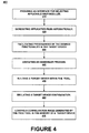
- FIG. 4 is a flow chart of a design tool process 400 , which illustrates exemplary steps used by a design tool in accordance with one embodiment of the present invention.
- One embodiment of an exemplary computer system utilized to implement design tool process 400 is set forth in incorporated U.S. patent application Ser. No. 09/989,570, filed Nov. 19, 2001, entitled “METHOD FOR FACILITATING MICROCONTROLLER PROGRAMMING”.
- Design tool process 400 facilitates configuration, programming, building, emulation and debugging of a customized “target device.”
- the target device is similar to integrated circuit 10 of FIG. 1 with a functional component 25 similar to FIG. 2 A.
- design tool process 400 is carried out by a computer system under the control of computer-readable and computer-executable instructions.
- the computer-readable and computer-executable instructions reside, for example, in data storage features of the computer system such as a computer usable volatile memory, computer-usable nonvolatile memory and/or data storage device.
- the computer-readable and computer-executable instructions direct computer system operations in accordance with design tool process 400 .
- a user module is a preconfigured function that may be based on more than one functional block.
- a user module when programmed and loaded on a memory of the target device directs a functional block to work as a peripheral on the target device.
- user modules may be added to or removed from the target device.
- the selected user modules are associated with (e.g., “placed” or “mapped to”) representations of functional blocks defined in the design tool. Once a user module is associated with a representation, its parameters can be viewed and modified as needed. Global parameters used by a plurality of user modules (for example, CPU clock speed) can also be set.
- interconnections between selected user modules are specified (e.g., either as each user module is placed or afterwards).
- the pin-out for each block can also be delineated, making a connection between the software configuration and the hardware of the target device.
- step 420 application files are automatically generated.
- application files are generated, existing assembly-source and C compiler code are updated for device configurations.
- APIs application program interfaces
- SRIs interrupt service routines
- step 430 programming of the desired functionality into the target device is facilitated.
- source code files can be edited, added or removed.
- programmable configuration of external device ports is also facilitated by design tool process 400 .
- an assembler process is executed.
- the assembler operates on an assembly-language source to produce executable code.
- This code is compiled and built into an executable file.
- the executable file is downloaded into an emulator, where the functionality of the target device will be emulated and debugged.
- step 450 the target device is “built” within the design tool. Building the target device in the design tool includes linking the programmed functionalities of the source files (including device configuration). In one exemplary implementation of the present invention, the linked programmed functionalities and the source files are downloaded to an emulator for debugging in step 450 .
- step 460 the target device is emulated using an in-circuit emulator for debugging.
- the emulator allows the target device to be tested in a hardware environment while device activity is viewed and debugged in a software environment.
- a configuration image generated using design tool process 400 is loaded into memory of a target device.
- a plurality of configuration images are loaded into memory of a target device.
- design tool process 400 of FIG. 4 Although specific steps are disclosed in design tool process 400 of FIG. 4 , such steps are exemplary. That is, the present invention is well suited to use with various other steps or variations of the steps recited in process 400 . Additionally, for purposes of clarity and brevity, the discussion is directed at times to specific examples.
- the present invention design tool process 400 is not limited solely to use to design a particular target device (e.g., a microcontroller). Instead, the present invention is well suited to use with other types of computer-aided hardware and software design systems in which it is necessary to accomplish a multitude of tasks as part of an overall process.
- FIG. 5 is a flow chart of one embodiment of a present invention boot sequence.
- the boot sequence is dictated by the information included in a boot file (e.g., boot.asm).
- a reset vector for the source code is originated after a target device is powered up.
- an interrupt table is held for code that is executed when an interrupt occurs.
- the interrupt table is held while a symbolic substitution process (e.g., step 330 of boot file creation method 300 ) is utilized to provide the appropriate interrupt service routine code.
- a boot table e.g., boot.tbl
- a boot table is used for automatic generation of interrupt vector table entries that map a user module interrupt to appropriate interrupt service routine code in a correct ROM location. Correct device configuration initialization successfully occurs because an appropriate substitution file that provides correct values and interrupt service routine code in the right location is created (e.g., with a call to LoadConfig) for each configuration change.
- some characteristics of the interrupt table are determined by the hardware of the target device.
- the hardware dictates that the interrupt entry points are 4 bytes apart beginning at program counter location zero (e.g., reset). Local jumps are enforced when an interrupt handler is originated (ORGed) within close proximity to (e.g., exactly at) the interrupt vectors. Therefore, a “long jump” (e.g., 3 byte long call) may be utilized and the vector table will not fall out of alignment (will not overrun into the next interrupt vector instruction).
- the present invention conveniently provides automatic interrupt routing based upon the selection and configuration of user modules.
- One example of correct automatic interrupt routing includes the exemplary long jump discussed above.
- a user module that requires 4 bytes of a different kind of code that is extremely fast is another example of an automatic interrupt service routine code generation that can be performed by the present invention.
- a present invention design tool has the ability to occupy the 4 bytes in an optimal manner for an interrupt. If the user module is moved (e.g., 5 blocks over) appropriate interrupt service routine code will automatically be generated by a present invention symbolic substitution process (e.g., boot file creation method 300 ) relieving the user from manually tracking and providing this information.
- step 530 device configuration initialization is called to enforce quick device configuration after reset.
- a proper “C” environment is created.
- a proper C environment is created to address certain types of initializations required by the “C” code.
- the “C” initialization is optionally provided even if the application is built using only assembly code.
- step 550 a main function is called to begin executing code.
- the boot file is regenerated every time device configurations change and application files are generated. In one embodiment of the present invention, this ensures that interrupt handles are consistent with the configuration.
- the application files change (e.g., due to changes in the configurations or functions of a device design) the boot.asm is regenerated to ensure that interrupt handlers are consistent with the configuration.
- the template file for the boot file e.g., boot.tpl template for boot.asm
- a user is permitted to hard code a change in boot.tpl file if a user does not want changes to a boot.asm file overwritten.
- the boot.asm file is constructed using the boot.tpl. For example, symbolic register names are replaced with the actual register names and appropriate interrupt vectors are mapped to their correct respective interrupt processing routines.
- the final boot.asm file is then completed. It is appreciated that the present invention substitution process is readily adaptable to a variety of applications, for example other source code files can also be automatically created using the present invention template procedure. The customer can easily modify the boot.tpl to insert their changes to boot.asm source without being lost during code generation.
Abstract
Description
Claims (19)
Priority Applications (1)
| Application Number | Priority Date | Filing Date | Title |
|---|---|---|---|
| US09/989,819 US6898703B1 (en) | 2001-11-19 | 2001-11-19 | System and method for creating a boot file utilizing a boot template |
Applications Claiming Priority (1)
| Application Number | Priority Date | Filing Date | Title |
|---|---|---|---|
| US09/989,819 US6898703B1 (en) | 2001-11-19 | 2001-11-19 | System and method for creating a boot file utilizing a boot template |
Publications (1)
| Publication Number | Publication Date |
|---|---|
| US6898703B1 true US6898703B1 (en) | 2005-05-24 |
Family
ID=34592834
Family Applications (1)
| Application Number | Title | Priority Date | Filing Date |
|---|---|---|---|
| US09/989,819 Expired - Lifetime US6898703B1 (en) | 2001-11-19 | 2001-11-19 | System and method for creating a boot file utilizing a boot template |
Country Status (1)
| Country | Link |
|---|---|
| US (1) | US6898703B1 (en) |
Cited By (62)
| Publication number | Priority date | Publication date | Assignee | Title |
|---|---|---|---|---|
| US20020108006A1 (en) * | 2000-10-26 | 2002-08-08 | Warren Snyder | Microcontroller programmable system on a chip |
| US20030153988A1 (en) * | 2002-02-12 | 2003-08-14 | Rusty Shepard | Highly versatile process control system controller |
| US20050027914A1 (en) * | 2003-07-31 | 2005-02-03 | Per Hammalund | Inter-processor interrupts |
| US20050038880A1 (en) * | 2003-07-14 | 2005-02-17 | Andrew Danforth | System and method for provisioning a provisionable network device with a dynamically generated boot file using a server |
| US20060033945A1 (en) * | 2004-08-13 | 2006-02-16 | Mcdonald John | Design model for a hardware device-independent method of defining embedded firmware for programmable systems |
| US20060037007A1 (en) * | 2004-08-13 | 2006-02-16 | Warren Snyder | Providing hardware independence to automate code generation of processing device firmware |
| US20060036973A1 (en) * | 2004-08-13 | 2006-02-16 | Kenneth Ogami | Method and an apparatus to design a processing system using a graphical user interface |
| US7219219B1 (en) * | 2004-01-13 | 2007-05-15 | Advanced Micro Devices, Inc. | Hardware initialization method that is independent of boot code architecture |
| US20070156715A1 (en) * | 2005-12-30 | 2007-07-05 | Thomas Mueller | Tagged property files for system configurations |
| US20070156641A1 (en) * | 2005-12-30 | 2007-07-05 | Thomas Mueller | System and method to provide system independent configuration references |
| US20070156432A1 (en) * | 2005-12-30 | 2007-07-05 | Thomas Mueller | Method and system using parameterized configurations |
| US20070156388A1 (en) * | 2005-12-30 | 2007-07-05 | Frank Kilian | Virtualized and adaptive configuration of a system |
| US20070156904A1 (en) * | 2005-12-30 | 2007-07-05 | Ingo Zenz | System and method for system information centralization |
| US20070156383A1 (en) * | 2005-12-30 | 2007-07-05 | Ingo Zenz | Calculated values in system configuration |
| US20070156717A1 (en) * | 2005-12-30 | 2007-07-05 | Ingo Zenz | Meta attributes of system configuration elements |
| US20070157010A1 (en) * | 2005-12-30 | 2007-07-05 | Ingo Zenz | Configuration templates for different use cases for a system |
| US20070157172A1 (en) * | 2005-12-30 | 2007-07-05 | Ingo Zenz | Template integration |
| US20070162892A1 (en) * | 2005-12-30 | 2007-07-12 | Ingo Zenz | Template-based configuration architecture |
| US20070165937A1 (en) * | 2005-12-30 | 2007-07-19 | Markov Mladen L | System and method for dynamic VM settings |
| US20070168965A1 (en) * | 2005-12-30 | 2007-07-19 | Ingo Zenz | Configuration inheritance in system configuration |
| US7287112B1 (en) * | 2001-11-19 | 2007-10-23 | Cypress Semiconductor Corporation | Dynamic reconfiguration interrupt system and method |
| US20070257715A1 (en) * | 2005-12-30 | 2007-11-08 | Semerdzhiev Krasimir P | System and method for abstract configuration |
| US20070273659A1 (en) * | 2006-05-26 | 2007-11-29 | Xiaoping Jiang | Multi-function slider in touchpad |
| US7308608B1 (en) | 2002-05-01 | 2007-12-11 | Cypress Semiconductor Corporation | Reconfigurable testing system and method |
| US20080258759A1 (en) * | 2007-04-17 | 2008-10-23 | Cypress Semiconductor Corporation | Universal digital block interconnection and channel routing |
| US20080259998A1 (en) * | 2007-04-17 | 2008-10-23 | Cypress Semiconductor Corp. | Temperature sensor with digital bandgap |
| US20080263334A1 (en) * | 2007-04-17 | 2008-10-23 | Cypress Semiconductor Corp. | Dynamically configurable and re-configurable data path |
| US20090066427A1 (en) * | 2005-02-04 | 2009-03-12 | Aaron Brennan | Poly-phase frequency synthesis oscillator |
| US20090183117A1 (en) * | 2003-12-12 | 2009-07-16 | Peter Hon-You Chang | Dynamic generation of target files from template files and tracking of the processing of target files |
| US7761845B1 (en) | 2002-09-09 | 2010-07-20 | Cypress Semiconductor Corporation | Method for parameterizing a user module |
| US7765095B1 (en) | 2000-10-26 | 2010-07-27 | Cypress Semiconductor Corporation | Conditional branching in an in-circuit emulation system |
| US7770113B1 (en) | 2001-11-19 | 2010-08-03 | Cypress Semiconductor Corporation | System and method for dynamically generating a configuration datasheet |
| US7774190B1 (en) | 2001-11-19 | 2010-08-10 | Cypress Semiconductor Corporation | Sleep and stall in an in-circuit emulation system |
| US7825688B1 (en) | 2000-10-26 | 2010-11-02 | Cypress Semiconductor Corporation | Programmable microcontroller architecture(mixed analog/digital) |
| US20100281145A1 (en) * | 2009-05-04 | 2010-11-04 | Cypress Semiconductor Corporation | Autonomous control in a programmable system |
| US7844437B1 (en) | 2001-11-19 | 2010-11-30 | Cypress Semiconductor Corporation | System and method for performing next placements and pruning of disallowed placements for programming an integrated circuit |
| US7893724B2 (en) | 2004-03-25 | 2011-02-22 | Cypress Semiconductor Corporation | Method and circuit for rapid alignment of signals |
| US8026739B2 (en) | 2007-04-17 | 2011-09-27 | Cypress Semiconductor Corporation | System level interconnect with programmable switching |
| US8040266B2 (en) | 2007-04-17 | 2011-10-18 | Cypress Semiconductor Corporation | Programmable sigma-delta analog-to-digital converter |
| US8042093B1 (en) | 2001-11-15 | 2011-10-18 | Cypress Semiconductor Corporation | System providing automatic source code generation for personalization and parameterization of user modules |
| US8049569B1 (en) | 2007-09-05 | 2011-11-01 | Cypress Semiconductor Corporation | Circuit and method for improving the accuracy of a crystal-less oscillator having dual-frequency modes |
| US8069405B1 (en) | 2001-11-19 | 2011-11-29 | Cypress Semiconductor Corporation | User interface for efficiently browsing an electronic document using data-driven tabs |
| US8067948B2 (en) | 2006-03-27 | 2011-11-29 | Cypress Semiconductor Corporation | Input/output multiplexer bus |
| US8069428B1 (en) | 2001-10-24 | 2011-11-29 | Cypress Semiconductor Corporation | Techniques for generating microcontroller configuration information |
| US8078894B1 (en) | 2007-04-25 | 2011-12-13 | Cypress Semiconductor Corporation | Power management architecture, method and configuration system |
| US8078970B1 (en) | 2001-11-09 | 2011-12-13 | Cypress Semiconductor Corporation | Graphical user interface with user-selectable list-box |
| US8085067B1 (en) | 2005-12-21 | 2011-12-27 | Cypress Semiconductor Corporation | Differential-to-single ended signal converter circuit and method |
| US8089461B2 (en) | 2005-06-23 | 2012-01-03 | Cypress Semiconductor Corporation | Touch wake for electronic devices |
| US8103497B1 (en) | 2002-03-28 | 2012-01-24 | Cypress Semiconductor Corporation | External interface for event architecture |
| US8103496B1 (en) | 2000-10-26 | 2012-01-24 | Cypress Semicondutor Corporation | Breakpoint control in an in-circuit emulation system |
| US8120408B1 (en) | 2005-05-05 | 2012-02-21 | Cypress Semiconductor Corporation | Voltage controlled oscillator delay cell and method |
| US8130025B2 (en) | 2007-04-17 | 2012-03-06 | Cypress Semiconductor Corporation | Numerical band gap |
| US8149048B1 (en) | 2000-10-26 | 2012-04-03 | Cypress Semiconductor Corporation | Apparatus and method for programmable power management in a programmable analog circuit block |
| US8160864B1 (en) | 2000-10-26 | 2012-04-17 | Cypress Semiconductor Corporation | In-circuit emulator and pod synchronized boot |
| US8201189B2 (en) | 2005-12-30 | 2012-06-12 | Sap Ag | System and method for filtering components |
| US8271769B2 (en) | 2005-12-30 | 2012-09-18 | Sap Ag | Dynamic adaptation of a configuration to a system environment |
| US8499270B1 (en) | 2007-04-25 | 2013-07-30 | Cypress Semiconductor Corporation | Configuration of programmable IC design elements |
| US8516025B2 (en) | 2007-04-17 | 2013-08-20 | Cypress Semiconductor Corporation | Clock driven dynamic datapath chaining |
| US8537121B2 (en) | 2006-05-26 | 2013-09-17 | Cypress Semiconductor Corporation | Multi-function slider in touchpad |
| US8843918B2 (en) | 2005-12-30 | 2014-09-23 | Sap Ag | System and method for deployable templates |
| US9720805B1 (en) | 2007-04-25 | 2017-08-01 | Cypress Semiconductor Corporation | System and method for controlling a target device |
| CN110968333A (en) * | 2018-09-30 | 2020-04-07 | 北京国双科技有限公司 | Configuration information replacement method and device, machine-readable storage medium and processor |
Citations (6)
| Publication number | Priority date | Publication date | Assignee | Title |
|---|---|---|---|---|
| US5544067A (en) * | 1990-04-06 | 1996-08-06 | Lsi Logic Corporation | Method and system for creating, deriving and validating structural description of electronic system from higher level, behavior-oriented description, including interactive schematic design and simulation |
| US6542844B1 (en) * | 2000-08-02 | 2003-04-01 | International Business Machines Corporation | Method and apparatus for tracing hardware states using dynamically reconfigurable test circuits |
| US6614320B1 (en) * | 2000-10-26 | 2003-09-02 | Cypress Semiconductor Corporation | System and method of providing a programmable clock architecture for an advanced microcontroller |
| US6724220B1 (en) * | 2000-10-26 | 2004-04-20 | Cyress Semiconductor Corporation | Programmable microcontroller architecture (mixed analog/digital) |
| US6732347B1 (en) * | 2001-04-26 | 2004-05-04 | Xilinx, Inc. | Clock template for configuring a programmable gate array |
| US6792584B1 (en) * | 2001-10-30 | 2004-09-14 | Lsi Logic Corporation | System and method for designing an integrated circuit |
-
2001
- 2001-11-19 US US09/989,819 patent/US6898703B1/en not_active Expired - Lifetime
Patent Citations (6)
| Publication number | Priority date | Publication date | Assignee | Title |
|---|---|---|---|---|
| US5544067A (en) * | 1990-04-06 | 1996-08-06 | Lsi Logic Corporation | Method and system for creating, deriving and validating structural description of electronic system from higher level, behavior-oriented description, including interactive schematic design and simulation |
| US6542844B1 (en) * | 2000-08-02 | 2003-04-01 | International Business Machines Corporation | Method and apparatus for tracing hardware states using dynamically reconfigurable test circuits |
| US6614320B1 (en) * | 2000-10-26 | 2003-09-02 | Cypress Semiconductor Corporation | System and method of providing a programmable clock architecture for an advanced microcontroller |
| US6724220B1 (en) * | 2000-10-26 | 2004-04-20 | Cyress Semiconductor Corporation | Programmable microcontroller architecture (mixed analog/digital) |
| US6732347B1 (en) * | 2001-04-26 | 2004-05-04 | Xilinx, Inc. | Clock template for configuring a programmable gate array |
| US6792584B1 (en) * | 2001-10-30 | 2004-09-14 | Lsi Logic Corporation | System and method for designing an integrated circuit |
Cited By (109)
| Publication number | Priority date | Publication date | Assignee | Title |
|---|---|---|---|---|
| US20020108006A1 (en) * | 2000-10-26 | 2002-08-08 | Warren Snyder | Microcontroller programmable system on a chip |
| US8358150B1 (en) | 2000-10-26 | 2013-01-22 | Cypress Semiconductor Corporation | Programmable microcontroller architecture(mixed analog/digital) |
| US9766650B2 (en) | 2000-10-26 | 2017-09-19 | Cypress Semiconductor Corporation | Microcontroller programmable system on a chip with programmable interconnect |
| US9843327B1 (en) | 2000-10-26 | 2017-12-12 | Cypress Semiconductor Corporation | PSOC architecture |
| US10020810B2 (en) | 2000-10-26 | 2018-07-10 | Cypress Semiconductor Corporation | PSoC architecture |
| US10248604B2 (en) | 2000-10-26 | 2019-04-02 | Cypress Semiconductor Corporation | Microcontroller programmable system on a chip |
| US7825688B1 (en) | 2000-10-26 | 2010-11-02 | Cypress Semiconductor Corporation | Programmable microcontroller architecture(mixed analog/digital) |
| US10261932B2 (en) | 2000-10-26 | 2019-04-16 | Cypress Semiconductor Corporation | Microcontroller programmable system on a chip |
| US8555032B2 (en) | 2000-10-26 | 2013-10-08 | Cypress Semiconductor Corporation | Microcontroller programmable system on a chip with programmable interconnect |
| US8160864B1 (en) | 2000-10-26 | 2012-04-17 | Cypress Semiconductor Corporation | In-circuit emulator and pod synchronized boot |
| US7765095B1 (en) | 2000-10-26 | 2010-07-27 | Cypress Semiconductor Corporation | Conditional branching in an in-circuit emulation system |
| US8103496B1 (en) | 2000-10-26 | 2012-01-24 | Cypress Semicondutor Corporation | Breakpoint control in an in-circuit emulation system |
| US10725954B2 (en) | 2000-10-26 | 2020-07-28 | Monterey Research, Llc | Microcontroller programmable system on a chip |
| US8736303B2 (en) | 2000-10-26 | 2014-05-27 | Cypress Semiconductor Corporation | PSOC architecture |
| US8149048B1 (en) | 2000-10-26 | 2012-04-03 | Cypress Semiconductor Corporation | Apparatus and method for programmable power management in a programmable analog circuit block |
| US8176296B2 (en) | 2000-10-26 | 2012-05-08 | Cypress Semiconductor Corporation | Programmable microcontroller architecture |
| US8793635B1 (en) | 2001-10-24 | 2014-07-29 | Cypress Semiconductor Corporation | Techniques for generating microcontroller configuration information |
| US8069428B1 (en) | 2001-10-24 | 2011-11-29 | Cypress Semiconductor Corporation | Techniques for generating microcontroller configuration information |
| US10466980B2 (en) | 2001-10-24 | 2019-11-05 | Cypress Semiconductor Corporation | Techniques for generating microcontroller configuration information |
| US8078970B1 (en) | 2001-11-09 | 2011-12-13 | Cypress Semiconductor Corporation | Graphical user interface with user-selectable list-box |
| US10698662B2 (en) | 2001-11-15 | 2020-06-30 | Cypress Semiconductor Corporation | System providing automatic source code generation for personalization and parameterization of user modules |
| US8042093B1 (en) | 2001-11-15 | 2011-10-18 | Cypress Semiconductor Corporation | System providing automatic source code generation for personalization and parameterization of user modules |
| US7770113B1 (en) | 2001-11-19 | 2010-08-03 | Cypress Semiconductor Corporation | System and method for dynamically generating a configuration datasheet |
| US7287112B1 (en) * | 2001-11-19 | 2007-10-23 | Cypress Semiconductor Corporation | Dynamic reconfiguration interrupt system and method |
| US7844437B1 (en) | 2001-11-19 | 2010-11-30 | Cypress Semiconductor Corporation | System and method for performing next placements and pruning of disallowed placements for programming an integrated circuit |
| US8370791B2 (en) | 2001-11-19 | 2013-02-05 | Cypress Semiconductor Corporation | System and method for performing next placements and pruning of disallowed placements for programming an integrated circuit |
| US8533677B1 (en) | 2001-11-19 | 2013-09-10 | Cypress Semiconductor Corporation | Graphical user interface for dynamically reconfiguring a programmable device |
| US8069405B1 (en) | 2001-11-19 | 2011-11-29 | Cypress Semiconductor Corporation | User interface for efficiently browsing an electronic document using data-driven tabs |
| US7774190B1 (en) | 2001-11-19 | 2010-08-10 | Cypress Semiconductor Corporation | Sleep and stall in an in-circuit emulation system |
| US6973508B2 (en) * | 2002-02-12 | 2005-12-06 | Fisher-Rosemount Systems, Inc. | Highly versatile process control system controller |
| US20060064512A1 (en) * | 2002-02-12 | 2006-03-23 | Fisher-Rosemount Systems, Inc. | Highly versatile process control system controller |
| US7181550B2 (en) | 2002-02-12 | 2007-02-20 | Fisher-Rosemount Systems, Inc. | Highly versatile process control system controller |
| US20030153988A1 (en) * | 2002-02-12 | 2003-08-14 | Rusty Shepard | Highly versatile process control system controller |
| US8103497B1 (en) | 2002-03-28 | 2012-01-24 | Cypress Semiconductor Corporation | External interface for event architecture |
| US7308608B1 (en) | 2002-05-01 | 2007-12-11 | Cypress Semiconductor Corporation | Reconfigurable testing system and method |
| US8402313B1 (en) | 2002-05-01 | 2013-03-19 | Cypress Semiconductor Corporation | Reconfigurable testing system and method |
| US7761845B1 (en) | 2002-09-09 | 2010-07-20 | Cypress Semiconductor Corporation | Method for parameterizing a user module |
| US20050038880A1 (en) * | 2003-07-14 | 2005-02-17 | Andrew Danforth | System and method for provisioning a provisionable network device with a dynamically generated boot file using a server |
| US7293078B2 (en) * | 2003-07-14 | 2007-11-06 | Time Warner Cable, A Division Of Time Warner Entertainment Company, L.P. | System and method for provisioning a provisionable network device with a dynamically generated boot file using a server |
| US20050027914A1 (en) * | 2003-07-31 | 2005-02-03 | Per Hammalund | Inter-processor interrupts |
| US8984199B2 (en) * | 2003-07-31 | 2015-03-17 | Intel Corporation | Inter-processor interrupts |
| US20090183117A1 (en) * | 2003-12-12 | 2009-07-16 | Peter Hon-You Chang | Dynamic generation of target files from template files and tracking of the processing of target files |
| US8346803B2 (en) | 2003-12-12 | 2013-01-01 | Knapp Investment Company Limited | Dynamic generation of target files from template files and tracking of the processing of target files |
| US7219219B1 (en) * | 2004-01-13 | 2007-05-15 | Advanced Micro Devices, Inc. | Hardware initialization method that is independent of boot code architecture |
| US7893724B2 (en) | 2004-03-25 | 2011-02-22 | Cypress Semiconductor Corporation | Method and circuit for rapid alignment of signals |
| US20060036973A1 (en) * | 2004-08-13 | 2006-02-16 | Kenneth Ogami | Method and an apparatus to design a processing system using a graphical user interface |
| US20060037007A1 (en) * | 2004-08-13 | 2006-02-16 | Warren Snyder | Providing hardware independence to automate code generation of processing device firmware |
| US20060033945A1 (en) * | 2004-08-13 | 2006-02-16 | Mcdonald John | Design model for a hardware device-independent method of defining embedded firmware for programmable systems |
| US8286125B2 (en) | 2004-08-13 | 2012-10-09 | Cypress Semiconductor Corporation | Model for a hardware device-independent method of defining embedded firmware for programmable systems |
| US8082531B2 (en) | 2004-08-13 | 2011-12-20 | Cypress Semiconductor Corporation | Method and an apparatus to design a processing system using a graphical user interface |
| US8069436B2 (en) | 2004-08-13 | 2011-11-29 | Cypress Semiconductor Corporation | Providing hardware independence to automate code generation of processing device firmware |
| US8539398B2 (en) | 2004-08-13 | 2013-09-17 | Cypress Semiconductor Corporation | Model for a hardware device-independent method of defining embedded firmware for programmable systems |
| US8085100B2 (en) | 2005-02-04 | 2011-12-27 | Cypress Semiconductor Corporation | Poly-phase frequency synthesis oscillator |
| US20090066427A1 (en) * | 2005-02-04 | 2009-03-12 | Aaron Brennan | Poly-phase frequency synthesis oscillator |
| US8120408B1 (en) | 2005-05-05 | 2012-02-21 | Cypress Semiconductor Corporation | Voltage controlled oscillator delay cell and method |
| US8089461B2 (en) | 2005-06-23 | 2012-01-03 | Cypress Semiconductor Corporation | Touch wake for electronic devices |
| US8085067B1 (en) | 2005-12-21 | 2011-12-27 | Cypress Semiconductor Corporation | Differential-to-single ended signal converter circuit and method |
| US20070165937A1 (en) * | 2005-12-30 | 2007-07-19 | Markov Mladen L | System and method for dynamic VM settings |
| US20070168965A1 (en) * | 2005-12-30 | 2007-07-19 | Ingo Zenz | Configuration inheritance in system configuration |
| US20070156715A1 (en) * | 2005-12-30 | 2007-07-05 | Thomas Mueller | Tagged property files for system configurations |
| US7954087B2 (en) | 2005-12-30 | 2011-05-31 | Sap Ag | Template integration |
| US7870538B2 (en) | 2005-12-30 | 2011-01-11 | Sap Ag | Configuration inheritance in system configuration |
| US7797522B2 (en) | 2005-12-30 | 2010-09-14 | Sap Ag | Meta attributes of system configuration elements |
| US7793087B2 (en) * | 2005-12-30 | 2010-09-07 | Sap Ag | Configuration templates for different use cases for a system |
| US8849894B2 (en) | 2005-12-30 | 2014-09-30 | Sap Ag | Method and system using parameterized configurations |
| US7779389B2 (en) | 2005-12-30 | 2010-08-17 | Sap Ag | System and method for dynamic VM settings |
| US7694117B2 (en) * | 2005-12-30 | 2010-04-06 | Sap Ag | Virtualized and adaptive configuration of a system |
| US7506145B2 (en) | 2005-12-30 | 2009-03-17 | Sap Ag | Calculated values in system configuration |
| US8843918B2 (en) | 2005-12-30 | 2014-09-23 | Sap Ag | System and method for deployable templates |
| US20070257715A1 (en) * | 2005-12-30 | 2007-11-08 | Semerdzhiev Krasimir P | System and method for abstract configuration |
| US9038023B2 (en) | 2005-12-30 | 2015-05-19 | Sap Se | Template-based configuration architecture |
| US20070162892A1 (en) * | 2005-12-30 | 2007-07-12 | Ingo Zenz | Template-based configuration architecture |
| US8201189B2 (en) | 2005-12-30 | 2012-06-12 | Sap Ag | System and method for filtering components |
| US8271769B2 (en) | 2005-12-30 | 2012-09-18 | Sap Ag | Dynamic adaptation of a configuration to a system environment |
| US20070157172A1 (en) * | 2005-12-30 | 2007-07-05 | Ingo Zenz | Template integration |
| US20070157010A1 (en) * | 2005-12-30 | 2007-07-05 | Ingo Zenz | Configuration templates for different use cases for a system |
| US20070156717A1 (en) * | 2005-12-30 | 2007-07-05 | Ingo Zenz | Meta attributes of system configuration elements |
| US20070156383A1 (en) * | 2005-12-30 | 2007-07-05 | Ingo Zenz | Calculated values in system configuration |
| US20070156904A1 (en) * | 2005-12-30 | 2007-07-05 | Ingo Zenz | System and method for system information centralization |
| US8838750B2 (en) | 2005-12-30 | 2014-09-16 | Sap Ag | System and method for system information centralization |
| US20070156388A1 (en) * | 2005-12-30 | 2007-07-05 | Frank Kilian | Virtualized and adaptive configuration of a system |
| US20070156432A1 (en) * | 2005-12-30 | 2007-07-05 | Thomas Mueller | Method and system using parameterized configurations |
| US20070156641A1 (en) * | 2005-12-30 | 2007-07-05 | Thomas Mueller | System and method to provide system independent configuration references |
| US8067948B2 (en) | 2006-03-27 | 2011-11-29 | Cypress Semiconductor Corporation | Input/output multiplexer bus |
| US8717042B1 (en) | 2006-03-27 | 2014-05-06 | Cypress Semiconductor Corporation | Input/output multiplexer bus |
| US20070273659A1 (en) * | 2006-05-26 | 2007-11-29 | Xiaoping Jiang | Multi-function slider in touchpad |
| US8089472B2 (en) | 2006-05-26 | 2012-01-03 | Cypress Semiconductor Corporation | Bidirectional slider with delete function |
| US8537121B2 (en) | 2006-05-26 | 2013-09-17 | Cypress Semiconductor Corporation | Multi-function slider in touchpad |
| US9564902B2 (en) | 2007-04-17 | 2017-02-07 | Cypress Semiconductor Corporation | Dynamically configurable and re-configurable data path |
| US20080263334A1 (en) * | 2007-04-17 | 2008-10-23 | Cypress Semiconductor Corp. | Dynamically configurable and re-configurable data path |
| US8130025B2 (en) | 2007-04-17 | 2012-03-06 | Cypress Semiconductor Corporation | Numerical band gap |
| US8092083B2 (en) | 2007-04-17 | 2012-01-10 | Cypress Semiconductor Corporation | Temperature sensor with digital bandgap |
| US20080258759A1 (en) * | 2007-04-17 | 2008-10-23 | Cypress Semiconductor Corporation | Universal digital block interconnection and channel routing |
| US20080259998A1 (en) * | 2007-04-17 | 2008-10-23 | Cypress Semiconductor Corp. | Temperature sensor with digital bandgap |
| US8476928B1 (en) | 2007-04-17 | 2013-07-02 | Cypress Semiconductor Corporation | System level interconnect with programmable switching |
| US7737724B2 (en) | 2007-04-17 | 2010-06-15 | Cypress Semiconductor Corporation | Universal digital block interconnection and channel routing |
| US8516025B2 (en) | 2007-04-17 | 2013-08-20 | Cypress Semiconductor Corporation | Clock driven dynamic datapath chaining |
| US8026739B2 (en) | 2007-04-17 | 2011-09-27 | Cypress Semiconductor Corporation | System level interconnect with programmable switching |
| US8040266B2 (en) | 2007-04-17 | 2011-10-18 | Cypress Semiconductor Corporation | Programmable sigma-delta analog-to-digital converter |
| US9720805B1 (en) | 2007-04-25 | 2017-08-01 | Cypress Semiconductor Corporation | System and method for controlling a target device |
| US8078894B1 (en) | 2007-04-25 | 2011-12-13 | Cypress Semiconductor Corporation | Power management architecture, method and configuration system |
| US8499270B1 (en) | 2007-04-25 | 2013-07-30 | Cypress Semiconductor Corporation | Configuration of programmable IC design elements |
| US8909960B1 (en) | 2007-04-25 | 2014-12-09 | Cypress Semiconductor Corporation | Power management architecture, method and configuration system |
| US8049569B1 (en) | 2007-09-05 | 2011-11-01 | Cypress Semiconductor Corporation | Circuit and method for improving the accuracy of a crystal-less oscillator having dual-frequency modes |
| US9880536B1 (en) | 2009-05-04 | 2018-01-30 | Cypress Semiconductor Corporation | Autonomous control in a programmable system |
| US20100281145A1 (en) * | 2009-05-04 | 2010-11-04 | Cypress Semiconductor Corporation | Autonomous control in a programmable system |
| US9448964B2 (en) * | 2009-05-04 | 2016-09-20 | Cypress Semiconductor Corporation | Autonomous control in a programmable system |
| CN110968333A (en) * | 2018-09-30 | 2020-04-07 | 北京国双科技有限公司 | Configuration information replacement method and device, machine-readable storage medium and processor |
| CN110968333B (en) * | 2018-09-30 | 2023-10-20 | 北京国双科技有限公司 | Configuration information replacement method and device, machine-readable storage medium and processor |
Similar Documents
| Publication | Publication Date | Title |
|---|---|---|
| US6898703B1 (en) | System and method for creating a boot file utilizing a boot template | |
| US6971004B1 (en) | System and method of dynamically reconfiguring a programmable integrated circuit | |
| US7024654B2 (en) | System and method for configuring analog elements in a configurable hardware device | |
| US10360327B2 (en) | Modifying a virtual processor model for hardware/software simulation | |
| US7308608B1 (en) | Reconfigurable testing system and method | |
| Sass et al. | Embedded systems design with platform FPGAs: principles and practices | |
| US6173438B1 (en) | Embedded graphical programming system | |
| US20040015502A1 (en) | Application program interface for programmable architecture cores | |
| CN112100954A (en) | Method and device for verifying chip and computer storage medium | |
| US7308396B2 (en) | Generating co-simulation and production executables from a single source | |
| US8042093B1 (en) | System providing automatic source code generation for personalization and parameterization of user modules | |
| Nolting | The neo430 processor | |
| US20020174266A1 (en) | Parameterized application programming interface for reconfigurable computing systems | |
| Kalb et al. | Enabling dynamic and partial reconfiguration in Xilinx SDSoC | |
| US7761845B1 (en) | Method for parameterizing a user module | |
| CN117480498A (en) | Dynamically provisioning PCIe devices for bare metal servers at run-time | |
| US11487927B2 (en) | Peripheral tool | |
| CN110442986B (en) | Method for managing server motherboard based on CPLD logic code generator | |
| Bogdanov et al. | Flash programming low power microcontrollers over the Internet | |
| US7130787B1 (en) | Functional replicator of a specific integrated circuit and its use as an emulation device | |
| Haron et al. | Internet of things platform on ARM/FPGA using embedded linux | |
| KR100557518B1 (en) | System large scale integrated circuitlsi, method of designing the same, and program therefor | |
| Developers | Verilog-to-routing documentation | |
| CN116954715A (en) | Transplanting method and device of processor platform, electronic equipment and medium | |
| Van | Integrating heterogeneous IoT devices to IoT Platform |
Legal Events
| Date | Code | Title | Description |
|---|---|---|---|
| AS | Assignment |
Owner name: CYPRESS SEMICONDUCTOR CORPORATION, CALIFORNIA Free format text: ASSIGNMENT OF ASSIGNORS INTEREST;ASSIGNORS:OGAMI, KENNETH Y.;PLEIS, MATTHEW A.;REEL/FRAME:012556/0305;SIGNING DATES FROM 20020103 TO 20020104 |
|
| STCF | Information on status: patent grant |
Free format text: PATENTED CASE |
|
| REMI | Maintenance fee reminder mailed | ||
| FEPP | Fee payment procedure |
Free format text: PAYER NUMBER DE-ASSIGNED (ORIGINAL EVENT CODE: RMPN); ENTITY STATUS OF PATENT OWNER: LARGE ENTITY Free format text: PAYOR NUMBER ASSIGNED (ORIGINAL EVENT CODE: ASPN); ENTITY STATUS OF PATENT OWNER: LARGE ENTITY |
|
| FPAY | Fee payment |
Year of fee payment: 4 |
|
| SULP | Surcharge for late payment | ||
| FPAY | Fee payment |
Year of fee payment: 8 |
|
| AS | Assignment |
Owner name: MORGAN STANLEY SENIOR FUNDING, INC., NEW YORK Free format text: SECURITY INTEREST;ASSIGNORS:CYPRESS SEMICONDUCTOR CORPORATION;SPANSION LLC;REEL/FRAME:035240/0429 Effective date: 20150312 |
|
| FPAY | Fee payment |
Year of fee payment: 12 |
|
| AS | Assignment |
Owner name: MUFG UNION BANK, N.A., CALIFORNIA Free format text: ASSIGNMENT AND ASSUMPTION OF SECURITY INTEREST IN INTELLECTUAL PROPERTY;ASSIGNOR:MORGAN STANLEY SENIOR FUNDING, INC.;REEL/FRAME:050896/0366 Effective date: 20190731 |
|
| AS | Assignment |
Owner name: MORGAN STANLEY SENIOR FUNDING, INC., NEW YORK Free format text: CORRECTIVE ASSIGNMENT TO CORRECT THE 8647899 PREVIOUSLY RECORDED ON REEL 035240 FRAME 0429. ASSIGNOR(S) HEREBY CONFIRMS THE SECURITY INTERST;ASSIGNORS:CYPRESS SEMICONDUCTOR CORPORATION;SPANSION LLC;REEL/FRAME:058002/0470 Effective date: 20150312 |
|
| AS | Assignment |
Owner name: SPANSION LLC, CALIFORNIA Free format text: RELEASE BY SECURED PARTY;ASSIGNOR:MUFG UNION BANK, N.A.;REEL/FRAME:059410/0438 Effective date: 20200416 Owner name: CYPRESS SEMICONDUCTOR CORPORATION, CALIFORNIA Free format text: RELEASE BY SECURED PARTY;ASSIGNOR:MUFG UNION BANK, N.A.;REEL/FRAME:059410/0438 Effective date: 20200416 |