US6881295B2 - Air-tight vessel equipped with gas feeder uniformly supplying gaseous component around plural wafers - Google Patents
Air-tight vessel equipped with gas feeder uniformly supplying gaseous component around plural wafers Download PDFInfo
- Publication number
- US6881295B2 US6881295B2 US09/819,516 US81951601A US6881295B2 US 6881295 B2 US6881295 B2 US 6881295B2 US 81951601 A US81951601 A US 81951601A US 6881295 B2 US6881295 B2 US 6881295B2
- Authority
- US
- United States
- Prior art keywords
- gas
- end surface
- treatment apparatus
- concave
- feeder
- Prior art date
- Legal status (The legal status is an assumption and is not a legal conclusion. Google has not performed a legal analysis and makes no representation as to the accuracy of the status listed.)
- Expired - Fee Related, expires
Links
Images


Classifications
-
- C—CHEMISTRY; METALLURGY
- C23—COATING METALLIC MATERIAL; COATING MATERIAL WITH METALLIC MATERIAL; CHEMICAL SURFACE TREATMENT; DIFFUSION TREATMENT OF METALLIC MATERIAL; COATING BY VACUUM EVAPORATION, BY SPUTTERING, BY ION IMPLANTATION OR BY CHEMICAL VAPOUR DEPOSITION, IN GENERAL; INHIBITING CORROSION OF METALLIC MATERIAL OR INCRUSTATION IN GENERAL
- C23C—COATING METALLIC MATERIAL; COATING MATERIAL WITH METALLIC MATERIAL; SURFACE TREATMENT OF METALLIC MATERIAL BY DIFFUSION INTO THE SURFACE, BY CHEMICAL CONVERSION OR SUBSTITUTION; COATING BY VACUUM EVAPORATION, BY SPUTTERING, BY ION IMPLANTATION OR BY CHEMICAL VAPOUR DEPOSITION, IN GENERAL
- C23C16/00—Chemical coating by decomposition of gaseous compounds, without leaving reaction products of surface material in the coating, i.e. chemical vapour deposition [CVD] processes
- C23C16/44—Chemical coating by decomposition of gaseous compounds, without leaving reaction products of surface material in the coating, i.e. chemical vapour deposition [CVD] processes characterised by the method of coating
- C23C16/455—Chemical coating by decomposition of gaseous compounds, without leaving reaction products of surface material in the coating, i.e. chemical vapour deposition [CVD] processes characterised by the method of coating characterised by the method used for introducing gases into reaction chamber or for modifying gas flows in reaction chamber
- C23C16/45563—Gas nozzles
-
- C—CHEMISTRY; METALLURGY
- C23—COATING METALLIC MATERIAL; COATING MATERIAL WITH METALLIC MATERIAL; CHEMICAL SURFACE TREATMENT; DIFFUSION TREATMENT OF METALLIC MATERIAL; COATING BY VACUUM EVAPORATION, BY SPUTTERING, BY ION IMPLANTATION OR BY CHEMICAL VAPOUR DEPOSITION, IN GENERAL; INHIBITING CORROSION OF METALLIC MATERIAL OR INCRUSTATION IN GENERAL
- C23C—COATING METALLIC MATERIAL; COATING MATERIAL WITH METALLIC MATERIAL; SURFACE TREATMENT OF METALLIC MATERIAL BY DIFFUSION INTO THE SURFACE, BY CHEMICAL CONVERSION OR SUBSTITUTION; COATING BY VACUUM EVAPORATION, BY SPUTTERING, BY ION IMPLANTATION OR BY CHEMICAL VAPOUR DEPOSITION, IN GENERAL
- C23C16/00—Chemical coating by decomposition of gaseous compounds, without leaving reaction products of surface material in the coating, i.e. chemical vapour deposition [CVD] processes
- C23C16/22—Chemical coating by decomposition of gaseous compounds, without leaving reaction products of surface material in the coating, i.e. chemical vapour deposition [CVD] processes characterised by the deposition of inorganic material, other than metallic material
- C23C16/30—Deposition of compounds, mixtures or solid solutions, e.g. borides, carbides, nitrides
- C23C16/40—Oxides
- C23C16/401—Oxides containing silicon
-
- C—CHEMISTRY; METALLURGY
- C23—COATING METALLIC MATERIAL; COATING MATERIAL WITH METALLIC MATERIAL; CHEMICAL SURFACE TREATMENT; DIFFUSION TREATMENT OF METALLIC MATERIAL; COATING BY VACUUM EVAPORATION, BY SPUTTERING, BY ION IMPLANTATION OR BY CHEMICAL VAPOUR DEPOSITION, IN GENERAL; INHIBITING CORROSION OF METALLIC MATERIAL OR INCRUSTATION IN GENERAL
- C23C—COATING METALLIC MATERIAL; COATING MATERIAL WITH METALLIC MATERIAL; SURFACE TREATMENT OF METALLIC MATERIAL BY DIFFUSION INTO THE SURFACE, BY CHEMICAL CONVERSION OR SUBSTITUTION; COATING BY VACUUM EVAPORATION, BY SPUTTERING, BY ION IMPLANTATION OR BY CHEMICAL VAPOUR DEPOSITION, IN GENERAL
- C23C16/00—Chemical coating by decomposition of gaseous compounds, without leaving reaction products of surface material in the coating, i.e. chemical vapour deposition [CVD] processes
- C23C16/44—Chemical coating by decomposition of gaseous compounds, without leaving reaction products of surface material in the coating, i.e. chemical vapour deposition [CVD] processes characterised by the method of coating
- C23C16/455—Chemical coating by decomposition of gaseous compounds, without leaving reaction products of surface material in the coating, i.e. chemical vapour deposition [CVD] processes characterised by the method of coating characterised by the method used for introducing gases into reaction chamber or for modifying gas flows in reaction chamber
- C23C16/45563—Gas nozzles
- C23C16/45574—Nozzles for more than one gas
-
- C—CHEMISTRY; METALLURGY
- C23—COATING METALLIC MATERIAL; COATING MATERIAL WITH METALLIC MATERIAL; CHEMICAL SURFACE TREATMENT; DIFFUSION TREATMENT OF METALLIC MATERIAL; COATING BY VACUUM EVAPORATION, BY SPUTTERING, BY ION IMPLANTATION OR BY CHEMICAL VAPOUR DEPOSITION, IN GENERAL; INHIBITING CORROSION OF METALLIC MATERIAL OR INCRUSTATION IN GENERAL
- C23C—COATING METALLIC MATERIAL; COATING MATERIAL WITH METALLIC MATERIAL; SURFACE TREATMENT OF METALLIC MATERIAL BY DIFFUSION INTO THE SURFACE, BY CHEMICAL CONVERSION OR SUBSTITUTION; COATING BY VACUUM EVAPORATION, BY SPUTTERING, BY ION IMPLANTATION OR BY CHEMICAL VAPOUR DEPOSITION, IN GENERAL
- C23C16/00—Chemical coating by decomposition of gaseous compounds, without leaving reaction products of surface material in the coating, i.e. chemical vapour deposition [CVD] processes
- C23C16/44—Chemical coating by decomposition of gaseous compounds, without leaving reaction products of surface material in the coating, i.e. chemical vapour deposition [CVD] processes characterised by the method of coating
- C23C16/455—Chemical coating by decomposition of gaseous compounds, without leaving reaction products of surface material in the coating, i.e. chemical vapour deposition [CVD] processes characterised by the method of coating characterised by the method used for introducing gases into reaction chamber or for modifying gas flows in reaction chamber
- C23C16/45563—Gas nozzles
- C23C16/45578—Elongated nozzles, tubes with holes
Definitions
- This invention relates to a gas treatment system and, more particularly, to a reactor or furnace incorporated in a gas treatment system used in the semiconductor manufacturing field.
- FIG. 1 shows a typical example of the vertical low-pressure chemical vapor deposition system.
- a reactor and a gas supply system (not shown) are incorporated in the prior art vertical low-pressure chemical vapor deposition system.
- the prior art reactor includes a base 1 , an outer tube 2 and an inner tube 3 .
- the base 1 is fixed to a horizontal foundation (not shown), and is upright thereon.
- the outer tube 2 is open at one end thereof, and is closed at the other end.
- the outer tube 2 is larger in diameter than the inner tube 3 , and is longer than the inner tube 3 .
- the inner tube 3 is open at both ends thereof.
- Gas inlet ports are formed in the outer tube 2 , and a gas outlet port is further formed in the outer tube 2 .
- the gas inlet ports and the gas outlet port are close to the open end of the outer tube 2 , and the gas outlet port is spaced from the gas inlet ports by 180 degrees.
- the inner tube 3 is partially cut away at one end portion thereof, and a hole is formed in one end portion of the inner tube 3 .
- the inner tube 3 is fixed to the base 1 , and is upright on the base 1 .
- the base 1 closes one end of the inner tube 3 .
- the inner tube 3 is inserted into the outer tube 2 in such a manner that the centerline of the outer tube 2 is coincident with the centerline of the inner tube 3 .
- the outer tube 2 is also fixed to the base 1 , and, accordingly, is upright on the base 1 .
- the inner tube 3 and the outer tube 2 forms a double structure on the base 1 .
- a cylindrical space is formed between the inner tube 3 and the outer tube 2 , and an upper space takes place between the closed end of the outer tube 2 and the other end of the inner tube 3 .
- the cylindrical space is connected through the upper space to the inner space of the inner tube 3 , and is further connected through the hole to the inner space of the inner tube 3 .
- the prior art reactor further comprises a boat holder 4 , heaters 7 a , 7 b and 7 c , a gas feeder 8 , an exhaust gas pipe 10 and inlet gas pipes 11 .
- the boat holder 4 is fixed to the base 1 , and is provided in the inner space of the inner tube 3 .
- the gas feeder 8 is provided in the inner space of the inner tube 3 , and vertically extends from the hole toward the other end of the inner tube 3 .
- the heaters 7 a , 7 b and 7 c are provided around the outer tube 2 , and, accordingly, the outer tube 2 is wrapped in the heaters 7 a , 7 b and 7 c .
- the gas supply system is connected through the inlet gas pipes 11 to the inlet gas ports of the outer tube 2 .
- One of the inlet gas pipes is open through the inlet gas port to the cylindrical space, and another inlet gas pipe is open to the hole formed in the inner tube 3 . Yet another inlet gas pipe is connected through the inlet gas port to the gas feeder 8 , and the exhaust pipe 10 is connected to the gas outlet port of the outer tube 2 . Though not shown in FIG. 1 , a pressure regulator is connected to the exhaust pipe 10 , and the pressure regulator keeps the pressure the in prior art reactor constant.
- a wafer boat 5 is put on the boat holder 4 , and semiconductor wafers 6 are supported by the wafer boat 5 at intervals.
- the gas feeder 8 is closed at the other end thereof, and gas outlet holes 9 are formed in the gas feeder 8 .
- the gas outlet holes 9 are equal in diameter, and are constant in density over the gas feeder 8 .
- the gas feeder 8 vertically extends, and gaseous mixture is blown from the gas outlet holes 9 to the semiconductor wafers.
- the gaseous mixture contains doping gas such as, for example, TMOB (Boron Tri-Methyl Ester) or phosphine, dilute gas such as nitrogen and vapor-phase growing gas such as TEOS (Tetra Ethyl Ortho-Silicate).
- the low-pressure chemical vapor deposition is carried out as follows.
- the semiconductor wafers 6 are supported by the wafer boat 5 , and the wafer boat 5 is placed on the boat holder 4 .
- the wafer boat 5 is vertically elongated in the vertical direction along the gas feeder 8 , and the gas outlet holes 9 are open to the semiconductor wafers 6 in the boat 5 .
- the heaters 7 a , 7 b and 7 c are energized, and raise the temperature inside the prior art reactor.
- the gaseous mixture is introduced into the inner space, and is maintained at target pressure.
- Substance such as, for example, silicon oxide is deposited over the semiconductor wafers 6 , and the dopant impurity is in situ introduced into the substance.
- the arrows AR are representative of the gas pressure. When the gas outlet holes 9 are spaced from the inlet end or the open end, the arrow AR becomes shorter. The lowest arrow AR is the longest of all, and the highest arrow AR is the shortest of all. This is because of the fact that the pressure is reduced from the open end toward the closed end. The higher the gas pressure is, the larger the flow-rate is. As a result, the concentration of the reactant gas is varied with the distance from the lower end of the gas feeder 8 . When a large amount of reactant gas is supplied to a semiconductor wafer, the deposition rate is increased. This results in the difference in thickness.
- the semiconductor wafers 6 are removed from both end portions of the wafer boat 5 , and are replaced with dummy wafers.
- the chemical vapor deposition is limited to the zone where the deposition rate is constantly controlled by means of the heaters 7 a , 7 b and 7 c . This results in reduction in the zone available for a single chemical vapor deposition.
- a solution is proposed in Japanese Patent Publication of Unexamined Application No. 58-197724.
- the prior art chemical vapor deposition system disclosed therein is equipped with a gas feeder 8 a , which is corresponding to the gas feeder 8 , shown in FIG. 3 .
- the gaseous mixture is blown from the gas feeder 8 a to semiconductor wafers supported by a wafer boat.
- a plurality of gas outlet holes 9 a / 9 b are formed in the prior art gas feeder 8 a as similar to the prior art gas feeder 8 .
- the gas outlet holes 9 a / 9 b are neither equal to diameter nor constant in density. The diameter is decreased from the open end toward the closed end, and the density of gas outlet holes 9 a / 9 b are increased toward the closed end.
- the diameter and the density are designed in such a manner that the gas flow rate is constant over the gas feeder 8 a . Since the gas concentration of the reactant gas is well controlled over the wafer boat, the deposition rate is substantially constant in the wafer boat. For this reason, any dummy wafer is not required for the prior art chemical vapor deposition reactor, and the throughput is maintained without sacrifice of the uniformity of the deposited substance.
- the small gas outlet holes 9 a are formed in the vicinity of the closed end of the gas feeder 8 a at high density, and the large gas outlet holes 9 b are formed in the vicinity of the open end of the gas feeder 8 a .
- the small holes are much more liable to be clogged with the by-products, and the prior art gas feeder 8 a requires cleaning frequently. If the cleaning is not frequently repeated, the semiconductor wafers are contaminated with the by-products, and the yield is lowered. Thus, the maintenance work is frequently required for removing the by-products from the prior art gas feeder 8 a .
- the large gas outlet holes 9 b makes the prior art gas feeder 8 a breakable, because the larger gas outlet holes 9 b seriously reduce the surface area of the open end portion of the prior art gas feeder 8 a .
- a new problem is encountered in the prior art chemical vapor deposition reactor equipped with the gas feeder 8 a in the maintenance works to be carried out at short intervals.
- the present invention proposes to gradually reduce the cross section of a gas passage defined in a gas feeder.
- a gas treatment apparatus comprising an outer tube having a gas inlet port connected to a gas supply system for receiving gas and a gas outlet port connected to an exhaust pipe and defining an inner space, a wafer boat provided in the inner space and holding plural wafers spaced from one another in a predetermined direction, an inner tube provided between the wafer boat and the outer tube and elongated in the predetermined direction, and a gas feeder provided between the inner tube and the wafer boat, connected to the gas inlet port and defining a gas passage gradually reduced in cross section in the predetermined direction and formed with gas outlet holes equal in open area and spaced in the predetermined direction for blowing the gas to the wafers.
- a gas treatment apparatus comprising an air-tight vessel having a gas inlet port connected to a gas supply system, a gas outlet port connected to an exhaust system and an inner space defined therein, a retainer provided in the inner space and retaining plural wafers arranged at intervals and a gas feeder connected at one end portion thereof to the gas inlet port and having a gas passage reduced in cross section from the one end portion toward another end portion of the gas feeder and plural gas outlet holes connected to the gas passage for blowing the gas toward the plural wafers.
- FIG. 1 is a schematic cross sectional view showing the structure of the prior art reactor
- FIG. 2 is a schematic cross sectional view showing the gas feeder incorporated in the prior art diffusion reactor
- FIG. 3 is a front view showing the gas feeder incorporated in the prior art chemical vapor deposition reactor disclosed in Japanese Patent Publication of Unexamined Application No. 58-197724;
- FIG. 4 is a schematic cross sectional view showing a reactor incorporated in a deposition system according to the present invention.
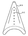
- FIG. 5 is a perspective view showing a gas feeder incorporated in the reactor
- FIG. 6 is a vertical cross sectional view showing the gas feeder incorporated in the reactor
- FIG. 7 is a horizontal cross sectional view showing the gas feeder incorporated in the reactor.
- FIG. 8 is a schematic view showing a dispersion of gas pressure inside of the gas feeder.
- a vertical low-pressure chemical vapor deposition system largely comprises a gas supply system, a vertical reactor and an exhaust system.
- the gas supply system includes sources of gas such as N 2 , TMOB or PH 3 and TEOS and gas supply pipes 11 , and these kinds of gas are supplied through the supply pipes 11 to the reactor.
- the exhaust system includes an exhaust pipe 10 , a pressure regulator (not shown) and a source of vacuum (not shown) such as, for example, a vacuum pump, and the exhaust system keeps the gas pressure inside of the reactor substantially constant.
- Doping gas, dilution gas and reactant gas are supplied from the gas supply system to the reactor.
- the doping gas may be boron trimethyl ester TMOB or phosphine PH 3 .
- the dilution gas may be nitrogen, and the reactant gas for deposited material may be tetraethylorthosilicate TEOS.
- the reactor includes a base structure 1 .
- the base structure 1 is broken down into a base plate and a circular rim.
- the base plate is placed on a horizontal foundation (not shown), and is anchored thereto.
- the circular rim is fixed to the upper surface of the base plate, and encircles a central area of the upper surface of the base plate.
- the reactor further includes an outer tube 2 and an inner tube 3 .
- the outer tube 2 is formed of quartz.
- the outer tube 2 is broken down into a shell and a head.
- the shell is tubular, and the head is attached to one end of the shell. For this reason, the outer tube 2 is closed at one end and open at the other end.
- An inner space is defined in the outer tube 2 .
- a inlet gas port and an outlet gas port are formed in the other end portion of the shell, and the gas inlet pipes 11 and the exhaust pipe 10 are to be connected to the inlet gas port and the outlet gas port, respectively.
- the shell is straight and constant in diameter.
- the head has a semi-spherical outer surface and a semi-spherical inner surface, and a recess is defined by the semi-spherical inner surface.
- the semi-spherical inner surface has a diameter equal to the inner diameter of the shell, and the semi-spherical outer surface has a diameter equal to the outer diameter of the shell. For this reason, the head is connected to the shell without any step therebetween, and prevents the outer tube 2 from the stress concentration.
- the outer tube 2 is placed on the circular rim of the base structure 1 , and is air-tightly connected to the rim of the base stricture 1 . Thus, the outer tube 2 is upright on the base structure 1 , and an inner space is defined inside the outer tube 2 .
- the inner tube 3 has a tubular configuration, and is less in diameter than the shell of the outer tube 2 .
- the inner tube 3 is constant in inner diameter, and is shorter than the outer tube 2 . No head is attached to the inner tube 3 , and, accordingly, the inner tube 3 is open at both ends thereof.
- the inner tube 3 is provided inside the outer tube 2 , and is connected to the base structure 1 .
- the inner tube 3 is upright on the base plate of the base structure 1 .
- a gap exists between the inner tube 3 and the outer tube 2 , and the inlet gas port and the outlet gas port are open to the tubular space between the inner tube 3 and the outer tube 2 .
- An opening is formed in one end portion of the inner tube 3 , and is close to the circular rim of the base structure 1 .
- the tubular space is connected to the inner space inside of the inner tube 3 through the opening.
- the reactor further included a boat holder 4 , heaters 7 a , 7 b and 7 c and a gas feeder 8 B.
- the boat holder 4 is provided inside the inner tube 3 , and is placed on the base plate of the base structure 1 .
- a tubular space exists between the inner tube 3 and the wafer boat 5 .
- the boat holder 4 is fixed to the base structure 1 , and a water boat 5 is to be put on the boat holder 4 .
- the semiconductor wafers 6 are supported by the wafer boat 5 .
- the wafer boat 5 is elongated in the vertical direction on the boat holder 4 , and semiconductor wafers 6 are spaced from one another in the wafer boat 5 in the vertical direction on the boat holder 4 .
- the heaters 7 a , 7 b and 7 c are attached to the shell of the outer tube 2 , and are connected to a controller (not shown).
- the heater 7 a is attached to the upper portion of the shell
- the heater 7 b is attached to the intermediate portion of the shell
- the heater 7 c is attached to the lower portion of the shell.
- the heaters 7 a , 7 b and 7 c are independently energized so as to control the temperature inside of the reactor.
- the heaters 7 a , 7 b and 7 c may make the temperature inside of the reactor substantially constant. If a temperature gradient is required, the controller energizes the heaters 7 a , 7 b and 7 c differently.
- the gas feeder 8 B is provided in the tubular space between the inner tube 3 and the wafer boat 5 , and vertically extends along the wafer boat 5 .
- An inner space is defined in the gas feeder 8 B, and also extends along the wafer boat 5 .
- the gas supply system is connected through the gas inlet port to the gas feeder 8 B, and the gas inlet port is formed at the lower end portion of the gas feeder 8 B.
- the upper end portion of the gas feeder 8 B is closed, and gas outlet holes 9 C are formed at regular intervals in the intermediate portion of the gas feeder 8 B.
- the gas outlet holes 9 are vertically spaced from one another, and are directed to the wafer boat 5 .
- the inner space in the gas feeder 8 B is gradually decreased in horizontal cross section from the lower end portion toward the upper end portion.
- Cones, frustums of cones, pyramids and frustums of pyramids are typical examples of the configuration gradually decreased in the cross section.
- it is impossible to place a cone-shaped or a pyramidal gas feeder inside the inner tube 3 because most of the inner space is occupied by the wafer boat 5 .
- the gas feeder 8 B is shaped into a part of the peripheral portion of a frustum of cone as shown in FIGS. 6 and 7 .
- the cross section is like a crescent (see FIG. 7 ).
- a convex surface, a concave surface and a pair of semi-cylindrical surfaces, an upper surface and bottom surface form the gas feeder 8 B.
- the gas outlet holes 9 C are formed in the concave surface along a virtual line, which is substantially in parallel to the vertical centerline of the wafer boat 5 .
- the gas outlet holes 9 C are equal in diameter, and are spaced at regular intervals.
- the diameter of the gas outlet holes 9 C is greater than that of the small gas outlet holes 9 a formed in the upper end portions of the gas feeder 8 a , and is less than that of the large gas outlet holes 9 b formed in the lower portion of the gas feeder 8 a of the prior art FIG. 3 .
- the gas outlet holes 9 C are easily formed in the gas feeder 8 B, and are less liable to be clogged with the by-products.
- the inner space of the gas feeder 8 B has a horizontal cross section, which is gradually decreased in area from the lower end toward the upper end. The inner space is designed in such a manner as to eliminate the pressure gradient from the gas in the inner space of the gas feeder 8 B.
- the gas pressure at all of the gas outlet holes 9 C is constant regardless of the position of the gas outlet holes 9 C as indicated by arrows (see FIG. 8 ). Since the gas outlet holes 9 C are equal in diameter to one another, the amount of gas blowing out from each gas outlet hole 9 C is approximately equal to that blowing out from another of the gas outlet holes 9 C.
- the doping gas is supplied from the gas supply system to the gas feeder 8 B, and is blown to the semiconductor wafers 6 in the wafer boat 5 for in-situ doping.
- the gas feeder 8 B uniformly supplies the doping gas to the semiconductor wafers 6 , and the dopant is uniformly introduced into the substance deposited on all the semiconductor wafers 6 .
- the heaters 7 a , 7 b and 7 c raises the temperature inside the reactor, and the pressure regulator (not shown) regulates the internal gas at a target pressure.
- the heaters 7 a , 7 b and 7 c keeps the gas at the target temperature, and the pressure regulator (not shown) keeps the internal gas at the target pressure.
- the reactant gas TEOS, the doping gas such as PH 3 and the dilution gas N 2 are supplied from the gas supply system through the gas pipes 11 to the reactor.
- the reactant gas TEOS is decomposed so that silicon oxide is deposited over the semiconductor wafers 6 .
- the doping gas PH 3 is supplied through the gas inlet port to the gas feeder 8 B, and is blown to the silicon oxide grown on the semiconductor wafers 6 .
- the phosphorous is introduced into the silicon oxide, and the phospho-silicate glass is grown on the semiconductor wafers 6 . Since the doping gas concentration is constant around the semiconductor wafers 6 in the wafer boat 5 , the phosphorous concentration is constant in the phospho-silicate glass deposited on all the semiconductor wafers 6 .
- the wafer holder 5 serves as a retainer, and said outer tube 2 and said inner tube 3 as a whole constitute an air-tight vessel.
- the gas feeder 8 B may be shaped into all the peripheral portion of a cone. In this instance, the wafer boat 5 is encircled with the gas feeder 8 B.
- the gas feeder 8 B maybe shaped into a part of or all of the peripheral portion of a pyramid.
- Reactant gas may be supplied to the gas feeder 8 B.
- the reactant gas concentration is uniform around the semiconductor wafers 5 in the wafer boat 5 , and the growth rate is constant on all the semiconductor wafers regardless of the position in the wafer boat 5 .
- the gas feeder 8 B may be incorporated in a thermal diffusion furnace.
- the dopant gas concentration is uniform around all the semiconductor wafers 5 , and the manufacturer achieves a target impurity profile in all the semiconductor wafers.
Landscapes
- Chemical & Material Sciences (AREA)
- General Chemical & Material Sciences (AREA)
- Chemical Kinetics & Catalysis (AREA)
- Engineering & Computer Science (AREA)
- Materials Engineering (AREA)
- Mechanical Engineering (AREA)
- Metallurgy (AREA)
- Organic Chemistry (AREA)
- Inorganic Chemistry (AREA)
- Chemical Vapour Deposition (AREA)
- Muffle Furnaces And Rotary Kilns (AREA)
- Furnace Details (AREA)
Abstract
Description
Claims (20)
Applications Claiming Priority (2)
| Application Number | Priority Date | Filing Date | Title |
|---|---|---|---|
| JP2000-89380 | 2000-03-28 | ||
| JP2000089380A JP2001274107A (en) | 2000-03-28 | 2000-03-28 | Diffusion furnace |
Publications (2)
| Publication Number | Publication Date |
|---|---|
| US20010025605A1 US20010025605A1 (en) | 2001-10-04 |
| US6881295B2 true US6881295B2 (en) | 2005-04-19 |
Family
ID=18605149
Family Applications (1)
| Application Number | Title | Priority Date | Filing Date |
|---|---|---|---|
| US09/819,516 Expired - Fee Related US6881295B2 (en) | 2000-03-28 | 2001-03-27 | Air-tight vessel equipped with gas feeder uniformly supplying gaseous component around plural wafers |
Country Status (3)
| Country | Link |
|---|---|
| US (1) | US6881295B2 (en) |
| JP (1) | JP2001274107A (en) |
| KR (1) | KR20010093721A (en) |
Cited By (38)
| Publication number | Priority date | Publication date | Assignee | Title |
|---|---|---|---|---|
| US20050028734A1 (en) * | 2003-02-11 | 2005-02-10 | Carpenter Craig M. | Reactors with isolated gas connectors and methods for depositing materials onto micro-device workpieces |
| US20050039686A1 (en) * | 2003-08-21 | 2005-02-24 | Zheng Lingyi A. | Microfeature workpiece processing apparatus and methods for batch deposition of materials on microfeature workpieces |
| US20050045102A1 (en) * | 2003-08-28 | 2005-03-03 | Zheng Lingyi A. | Methods and apparatus for processing microfeature workpieces, e.g., for depositing materials on microfeature workpieces |
| US20050287806A1 (en) * | 2004-06-24 | 2005-12-29 | Hiroyuki Matsuura | Vertical CVD apparatus and CVD method using the same |
| US7258892B2 (en) | 2003-12-10 | 2007-08-21 | Micron Technology, Inc. | Methods and systems for controlling temperature during microfeature workpiece processing, e.g., CVD deposition |
| USD552047S1 (en) * | 2005-02-28 | 2007-10-02 | Tokyo Electron Limited | Process tube for manufacturing semiconductor wafers |
| US7279398B2 (en) | 2003-09-17 | 2007-10-09 | Micron Technology, Inc. | Microfeature workpiece processing apparatus and methods for controlling deposition of materials on microfeature workpieces |
| US7282239B2 (en) | 2003-09-18 | 2007-10-16 | Micron Technology, Inc. | Systems and methods for depositing material onto microfeature workpieces in reaction chambers |
| US7323231B2 (en) | 2003-10-09 | 2008-01-29 | Micron Technology, Inc. | Apparatus and methods for plasma vapor deposition processes |
| US7335396B2 (en) | 2003-04-24 | 2008-02-26 | Micron Technology, Inc. | Methods for controlling mass flow rates and pressures in passageways coupled to reaction chambers and systems for depositing material onto microfeature workpieces in reaction chambers |
| US7344755B2 (en) | 2003-08-21 | 2008-03-18 | Micron Technology, Inc. | Methods and apparatus for processing microfeature workpieces; methods for conditioning ALD reaction chambers |
| US20080083372A1 (en) * | 2006-08-04 | 2008-04-10 | Hisashi Inoue | Heat processing apparatus for semiconductor process |
| US7387685B2 (en) | 2002-07-08 | 2008-06-17 | Micron Technology, Inc. | Apparatus and method for depositing materials onto microelectronic workpieces |
| US7481887B2 (en) | 2002-05-24 | 2009-01-27 | Micron Technology, Inc. | Apparatus for controlling gas pulsing in processes for depositing materials onto micro-device workpieces |
| US20090162262A1 (en) * | 2007-12-19 | 2009-06-25 | Applied Material, Inc. | Plasma reactor gas distribution plate having path splitting manifold side-by-side with showerhead |
| US20090162261A1 (en) * | 2007-12-19 | 2009-06-25 | Kallol Baera | Plasma reactor gas distribution plate having a vertically stacked path splitting manifold |
| US20090162260A1 (en) * | 2007-12-19 | 2009-06-25 | Kallol Bera | Plasma reactor gas distribution plate with radially distributed path splitting manifold |
| US20090159002A1 (en) * | 2007-12-19 | 2009-06-25 | Kallol Bera | Gas distribution plate with annular plenum having a sloped ceiling for uniform distribution |
| US20090159213A1 (en) * | 2007-12-19 | 2009-06-25 | Applied Materials, Inc. | Plasma reactor gas distribution plate having a path splitting manifold immersed within a showerhead |
| US7581511B2 (en) | 2003-10-10 | 2009-09-01 | Micron Technology, Inc. | Apparatus and methods for manufacturing microfeatures on workpieces using plasma vapor processes |
| US7584942B2 (en) | 2004-03-31 | 2009-09-08 | Micron Technology, Inc. | Ampoules for producing a reaction gas and systems for depositing materials onto microfeature workpieces in reaction chambers |
| US7588804B2 (en) | 2002-08-15 | 2009-09-15 | Micron Technology, Inc. | Reactors with isolated gas connectors and methods for depositing materials onto micro-device workpieces |
| USD610559S1 (en) * | 2008-05-30 | 2010-02-23 | Hitachi Kokusai Electric, Inc. | Reaction tube |
| US7699932B2 (en) | 2004-06-02 | 2010-04-20 | Micron Technology, Inc. | Reactors, systems and methods for depositing thin films onto microfeature workpieces |
| US20100218725A1 (en) * | 2009-02-27 | 2010-09-02 | Mrl Industries, Inc. | Apparatus for manufacture of solar cells |
| US20110048933A1 (en) * | 2009-08-28 | 2011-03-03 | Hon Hai Precision Industry Co., Ltd. | Gas-inputting device for vacuum sputtering apparatus |
| CN102242344A (en) * | 2010-05-13 | 2011-11-16 | 鸿富锦精密工业(深圳)有限公司 | Sputtering apparatus |
| US20110278164A1 (en) * | 2010-05-12 | 2011-11-17 | Hon Hai Precision Industry Co., Ltd. | Sputtering device |
| US8133554B2 (en) | 2004-05-06 | 2012-03-13 | Micron Technology, Inc. | Methods for depositing material onto microfeature workpieces in reaction chambers and systems for depositing materials onto microfeature workpieces |
| US20120180727A1 (en) * | 2010-12-22 | 2012-07-19 | Tokyo Electron Limited | Film forming apparatus |
| US20120240348A1 (en) * | 2002-03-28 | 2012-09-27 | Kazuyuki Okuda | Substrate processing apparatus |
| US20130167774A1 (en) * | 2012-01-03 | 2013-07-04 | Cheol-Kyu Yang | Batch type apparatus for manufacturing semiconductor devices |
| US20140345801A1 (en) * | 2011-11-17 | 2014-11-27 | Eugene Technology Co., Ltd. | Apparatus for processing substrate for supplying reaction gas having phase difference |
| US20150013909A1 (en) * | 2011-11-17 | 2015-01-15 | Eugene Technology Co., Ltd. | Substrate processing apparatus including auxiliary gas supply port |
| US10422035B2 (en) * | 2012-12-18 | 2019-09-24 | Tokyo Electron Limited | Thin film forming method and thin film forming appartus |
| US10453735B2 (en) * | 2017-09-26 | 2019-10-22 | Kokusai Electric Corporation | Substrate processing apparatus, reaction tube, semiconductor device manufacturing method, and recording medium |
| US11450524B2 (en) * | 2017-03-24 | 2022-09-20 | Kokusai Electric Corporation | Substrate processing apparatus, method of manufacturing semiconductor device, and recording medium |
| US12325916B2 (en) | 2021-08-13 | 2025-06-10 | Samsung Electronics Co., Ltd. | Film forming apparatus |
Families Citing this family (26)
| Publication number | Priority date | Publication date | Assignee | Title |
|---|---|---|---|---|
| KR100560867B1 (en) * | 2000-05-02 | 2006-03-13 | 동경 엘렉트론 주식회사 | Oxidation Method and Oxidation System |
| JP3980840B2 (en) * | 2001-04-25 | 2007-09-26 | 東京エレクトロン株式会社 | Vapor growth apparatus and vapor growth film forming method |
| KR100444753B1 (en) * | 2001-11-14 | 2004-08-21 | 국제엘렉트릭코리아 주식회사 | Deposition apparatus for manufacturing semiconductor devices |
| KR100829327B1 (en) * | 2002-04-05 | 2008-05-13 | 가부시키가이샤 히다치 고쿠사이 덴키 | Substrate Processing Unit and Reaction Vessel |
| JP4413562B2 (en) * | 2003-09-05 | 2010-02-10 | 東京エレクトロン株式会社 | Processing system and processing method |
| DE102004004858A1 (en) * | 2004-01-30 | 2005-08-18 | Infineon Technologies Ag | Implements for simultaneously coating number of wafers during semiconductor manufacture by deposition from gas phase, i.e. chemical vapour deposition (CVD), or compressing chemical vapour deposition (LPCVD) as well as gas injector |
| JP4455225B2 (en) * | 2004-08-25 | 2010-04-21 | Necエレクトロニクス株式会社 | Manufacturing method of semiconductor device |
| US7966969B2 (en) * | 2004-09-22 | 2011-06-28 | Asm International N.V. | Deposition of TiN films in a batch reactor |
| US8251012B2 (en) * | 2005-03-01 | 2012-08-28 | Hitachi Kokusai Electric Inc. | Substrate processing apparatus and semiconductor device producing method |
| JPWO2007111348A1 (en) * | 2006-03-28 | 2009-08-13 | 株式会社日立国際電気 | Substrate processing equipment |
| US7691757B2 (en) | 2006-06-22 | 2010-04-06 | Asm International N.V. | Deposition of complex nitride films |
| US7629256B2 (en) | 2007-05-14 | 2009-12-08 | Asm International N.V. | In situ silicon and titanium nitride deposition |
| JP5568212B2 (en) * | 2007-09-19 | 2014-08-06 | 株式会社日立国際電気 | Substrate processing apparatus, coating method therefor, substrate processing method, and semiconductor device manufacturing method |
| CN101488446B (en) | 2008-01-14 | 2010-09-01 | 北京北方微电子基地设备工艺研究中心有限责任公司 | Plasma processing equipment and its gas distribution device |
| KR101431197B1 (en) * | 2008-01-24 | 2014-09-17 | 삼성전자주식회사 | Atomic layer deposition equipment and atomic layer deposition method thereof |
| JP2009203533A (en) * | 2008-02-28 | 2009-09-10 | Nec Electronics Corp | Atomic layer epitaxy apparatus |
| US7833906B2 (en) | 2008-12-11 | 2010-11-16 | Asm International N.V. | Titanium silicon nitride deposition |
| US8409352B2 (en) * | 2010-03-01 | 2013-04-02 | Hitachi Kokusai Electric Inc. | Method of manufacturing semiconductor device, method of manufacturing substrate and substrate processing apparatus |
| JP5595963B2 (en) * | 2011-03-31 | 2014-09-24 | 東京エレクトロン株式会社 | Vertical batch deposition system |
| JP2013163841A (en) * | 2012-02-10 | 2013-08-22 | Jtekt Corp | Carbon film forming apparatus and carbon film forming method |
| CN109237941A (en) * | 2018-10-30 | 2019-01-18 | 湖南金炉科技股份有限公司 | bell-type furnace |
| KR102782608B1 (en) | 2019-10-14 | 2025-03-14 | 삼성전자주식회사 | Semiconductor manufacturing apparatus |
| KR20210129598A (en) * | 2020-04-17 | 2021-10-28 | 에이에스엠 아이피 홀딩 비.브이. | Injector configured for arrangement within a reactor of a vertical furnace and vertical furnace |
| CN113755823B (en) * | 2021-09-07 | 2023-10-13 | 北京北方华创微电子装备有限公司 | Gas injection device for semiconductor heat treatment equipment and semiconductor heat treatment equipment |
| CN119800332B (en) * | 2025-03-13 | 2025-07-04 | 盛美半导体设备(上海)股份有限公司 | Inlet pipe and furnace pipe equipment |
| CN121109987B (en) * | 2025-11-12 | 2026-02-27 | 中国人民解放军国防科技大学 | Preparation method and system for sapphire coated atomic air chamber |
Citations (17)
| Publication number | Priority date | Publication date | Assignee | Title |
|---|---|---|---|---|
| US3777987A (en) * | 1972-08-04 | 1973-12-11 | Allport Davies | Irrigation device |
| JPS58197724A (en) | 1982-05-12 | 1983-11-17 | Toshiba Corp | Gas introducing tube for vapor growth apparatus |
| US5029598A (en) * | 1989-04-21 | 1991-07-09 | Hoechst Aktiengesellschaft | Process for the uniform introduction of a fluid, and apparatus for carrying out the process |
| JPH03228320A (en) | 1990-02-02 | 1991-10-09 | Nkk Corp | Thin film forming equipment |
| JPH03263824A (en) | 1990-03-14 | 1991-11-25 | Mitsubishi Electric Corp | Wafer treatment boat |
| JPH0410531A (en) | 1990-04-27 | 1992-01-14 | Toshiba Ceramics Co Ltd | Vertical diffusion furnace |
| US5164012A (en) * | 1990-01-12 | 1992-11-17 | Tokyo Electron Limited | Heat treatment apparatus and method of forming a thin film using the apparatus |
| JPH0758030A (en) * | 1993-08-18 | 1995-03-03 | Toshiba Corp | Semiconductor manufacturing equipment |
| US5441570A (en) * | 1993-06-22 | 1995-08-15 | Jein Technics Co., Ltd. | Apparatus for low pressure chemical vapor deposition |
| JPH07297132A (en) | 1994-04-21 | 1995-11-10 | Hitachi Ltd | Vapor phase growth equipment |
| US5500388A (en) * | 1993-06-30 | 1996-03-19 | Tokyo Electron Kabushiki Kaisha | Heat treatment process for wafers |
| US5505385A (en) * | 1994-07-29 | 1996-04-09 | Pneumafil Corporation | Laminar air diffuser |
| JPH0997768A (en) | 1995-09-28 | 1997-04-08 | Nec Kyushu Ltd | Vertical diffusion oven |
| US5618349A (en) * | 1993-07-24 | 1997-04-08 | Yamaha Corporation | Thermal treatment with enhanced intra-wafer, intra-and inter-batch uniformity |
| US5704981A (en) * | 1995-04-05 | 1998-01-06 | Tokyo Electron Ltd. | Processing apparatus for substrates to be processed |
| JPH116068A (en) * | 1997-06-17 | 1999-01-12 | Nec Kyushu Ltd | Low pressure vapor growth equipment |
| US6352084B1 (en) * | 1996-10-24 | 2002-03-05 | Steag Microtech Gmbh | Substrate treatment device |
-
2000
- 2000-03-28 JP JP2000089380A patent/JP2001274107A/en active Pending
-
2001
- 2001-03-27 KR KR1020010016039A patent/KR20010093721A/en not_active Ceased
- 2001-03-27 US US09/819,516 patent/US6881295B2/en not_active Expired - Fee Related
Patent Citations (17)
| Publication number | Priority date | Publication date | Assignee | Title |
|---|---|---|---|---|
| US3777987A (en) * | 1972-08-04 | 1973-12-11 | Allport Davies | Irrigation device |
| JPS58197724A (en) | 1982-05-12 | 1983-11-17 | Toshiba Corp | Gas introducing tube for vapor growth apparatus |
| US5029598A (en) * | 1989-04-21 | 1991-07-09 | Hoechst Aktiengesellschaft | Process for the uniform introduction of a fluid, and apparatus for carrying out the process |
| US5164012A (en) * | 1990-01-12 | 1992-11-17 | Tokyo Electron Limited | Heat treatment apparatus and method of forming a thin film using the apparatus |
| JPH03228320A (en) | 1990-02-02 | 1991-10-09 | Nkk Corp | Thin film forming equipment |
| JPH03263824A (en) | 1990-03-14 | 1991-11-25 | Mitsubishi Electric Corp | Wafer treatment boat |
| JPH0410531A (en) | 1990-04-27 | 1992-01-14 | Toshiba Ceramics Co Ltd | Vertical diffusion furnace |
| US5441570A (en) * | 1993-06-22 | 1995-08-15 | Jein Technics Co., Ltd. | Apparatus for low pressure chemical vapor deposition |
| US5500388A (en) * | 1993-06-30 | 1996-03-19 | Tokyo Electron Kabushiki Kaisha | Heat treatment process for wafers |
| US5618349A (en) * | 1993-07-24 | 1997-04-08 | Yamaha Corporation | Thermal treatment with enhanced intra-wafer, intra-and inter-batch uniformity |
| JPH0758030A (en) * | 1993-08-18 | 1995-03-03 | Toshiba Corp | Semiconductor manufacturing equipment |
| JPH07297132A (en) | 1994-04-21 | 1995-11-10 | Hitachi Ltd | Vapor phase growth equipment |
| US5505385A (en) * | 1994-07-29 | 1996-04-09 | Pneumafil Corporation | Laminar air diffuser |
| US5704981A (en) * | 1995-04-05 | 1998-01-06 | Tokyo Electron Ltd. | Processing apparatus for substrates to be processed |
| JPH0997768A (en) | 1995-09-28 | 1997-04-08 | Nec Kyushu Ltd | Vertical diffusion oven |
| US6352084B1 (en) * | 1996-10-24 | 2002-03-05 | Steag Microtech Gmbh | Substrate treatment device |
| JPH116068A (en) * | 1997-06-17 | 1999-01-12 | Nec Kyushu Ltd | Low pressure vapor growth equipment |
Cited By (57)
| Publication number | Priority date | Publication date | Assignee | Title |
|---|---|---|---|---|
| US20120240348A1 (en) * | 2002-03-28 | 2012-09-27 | Kazuyuki Okuda | Substrate processing apparatus |
| US20130133696A1 (en) * | 2002-03-28 | 2013-05-30 | Hitachi Kokusai Electric Inc. | Substrate processing apparatus |
| US8366868B2 (en) * | 2002-03-28 | 2013-02-05 | Hitachi Kokusai Electric Inc. | Substrate processing apparatus |
| US7481887B2 (en) | 2002-05-24 | 2009-01-27 | Micron Technology, Inc. | Apparatus for controlling gas pulsing in processes for depositing materials onto micro-device workpieces |
| US7387685B2 (en) | 2002-07-08 | 2008-06-17 | Micron Technology, Inc. | Apparatus and method for depositing materials onto microelectronic workpieces |
| US7588804B2 (en) | 2002-08-15 | 2009-09-15 | Micron Technology, Inc. | Reactors with isolated gas connectors and methods for depositing materials onto micro-device workpieces |
| US7427425B2 (en) | 2003-02-11 | 2008-09-23 | Micron Technology, Inc. | Reactors with isolated gas connectors and methods for depositing materials onto micro-device workpieces |
| US20050028734A1 (en) * | 2003-02-11 | 2005-02-10 | Carpenter Craig M. | Reactors with isolated gas connectors and methods for depositing materials onto micro-device workpieces |
| US7335396B2 (en) | 2003-04-24 | 2008-02-26 | Micron Technology, Inc. | Methods for controlling mass flow rates and pressures in passageways coupled to reaction chambers and systems for depositing material onto microfeature workpieces in reaction chambers |
| US7344755B2 (en) | 2003-08-21 | 2008-03-18 | Micron Technology, Inc. | Methods and apparatus for processing microfeature workpieces; methods for conditioning ALD reaction chambers |
| US20050039686A1 (en) * | 2003-08-21 | 2005-02-24 | Zheng Lingyi A. | Microfeature workpiece processing apparatus and methods for batch deposition of materials on microfeature workpieces |
| US7235138B2 (en) * | 2003-08-21 | 2007-06-26 | Micron Technology, Inc. | Microfeature workpiece processing apparatus and methods for batch deposition of materials on microfeature workpieces |
| US20050045102A1 (en) * | 2003-08-28 | 2005-03-03 | Zheng Lingyi A. | Methods and apparatus for processing microfeature workpieces, e.g., for depositing materials on microfeature workpieces |
| US7422635B2 (en) | 2003-08-28 | 2008-09-09 | Micron Technology, Inc. | Methods and apparatus for processing microfeature workpieces, e.g., for depositing materials on microfeature workpieces |
| US7279398B2 (en) | 2003-09-17 | 2007-10-09 | Micron Technology, Inc. | Microfeature workpiece processing apparatus and methods for controlling deposition of materials on microfeature workpieces |
| US7282239B2 (en) | 2003-09-18 | 2007-10-16 | Micron Technology, Inc. | Systems and methods for depositing material onto microfeature workpieces in reaction chambers |
| US7323231B2 (en) | 2003-10-09 | 2008-01-29 | Micron Technology, Inc. | Apparatus and methods for plasma vapor deposition processes |
| US7581511B2 (en) | 2003-10-10 | 2009-09-01 | Micron Technology, Inc. | Apparatus and methods for manufacturing microfeatures on workpieces using plasma vapor processes |
| US7258892B2 (en) | 2003-12-10 | 2007-08-21 | Micron Technology, Inc. | Methods and systems for controlling temperature during microfeature workpiece processing, e.g., CVD deposition |
| US7771537B2 (en) | 2003-12-10 | 2010-08-10 | Micron Technology, Inc. | Methods and systems for controlling temperature during microfeature workpiece processing, E.G. CVD deposition |
| US8518184B2 (en) | 2003-12-10 | 2013-08-27 | Micron Technology, Inc. | Methods and systems for controlling temperature during microfeature workpiece processing, E.G., CVD deposition |
| US7584942B2 (en) | 2004-03-31 | 2009-09-08 | Micron Technology, Inc. | Ampoules for producing a reaction gas and systems for depositing materials onto microfeature workpieces in reaction chambers |
| US8133554B2 (en) | 2004-05-06 | 2012-03-13 | Micron Technology, Inc. | Methods for depositing material onto microfeature workpieces in reaction chambers and systems for depositing materials onto microfeature workpieces |
| US9023436B2 (en) | 2004-05-06 | 2015-05-05 | Micron Technology, Inc. | Methods for depositing material onto microfeature workpieces in reaction chambers and systems for depositing materials onto microfeature workpieces |
| US7699932B2 (en) | 2004-06-02 | 2010-04-20 | Micron Technology, Inc. | Reactors, systems and methods for depositing thin films onto microfeature workpieces |
| US20050287806A1 (en) * | 2004-06-24 | 2005-12-29 | Hiroyuki Matsuura | Vertical CVD apparatus and CVD method using the same |
| US7927662B2 (en) | 2004-06-24 | 2011-04-19 | Tokyo Electron Limited | CVD method in vertical CVD apparatus using different reactive gases |
| US20080213478A1 (en) * | 2004-06-24 | 2008-09-04 | Tokyo Electron Limited | Vertical cvd apparatus and cvd method using the same |
| USD552047S1 (en) * | 2005-02-28 | 2007-10-02 | Tokyo Electron Limited | Process tube for manufacturing semiconductor wafers |
| US8002895B2 (en) * | 2006-08-04 | 2011-08-23 | Tokyo Electron Limited | Heat processing apparatus for semiconductor process |
| US20080083372A1 (en) * | 2006-08-04 | 2008-04-10 | Hisashi Inoue | Heat processing apparatus for semiconductor process |
| US20090159002A1 (en) * | 2007-12-19 | 2009-06-25 | Kallol Bera | Gas distribution plate with annular plenum having a sloped ceiling for uniform distribution |
| US20090162260A1 (en) * | 2007-12-19 | 2009-06-25 | Kallol Bera | Plasma reactor gas distribution plate with radially distributed path splitting manifold |
| US8512509B2 (en) | 2007-12-19 | 2013-08-20 | Applied Materials, Inc. | Plasma reactor gas distribution plate with radially distributed path splitting manifold |
| US20090159213A1 (en) * | 2007-12-19 | 2009-06-25 | Applied Materials, Inc. | Plasma reactor gas distribution plate having a path splitting manifold immersed within a showerhead |
| US20090162262A1 (en) * | 2007-12-19 | 2009-06-25 | Applied Material, Inc. | Plasma reactor gas distribution plate having path splitting manifold side-by-side with showerhead |
| US20090162261A1 (en) * | 2007-12-19 | 2009-06-25 | Kallol Baera | Plasma reactor gas distribution plate having a vertically stacked path splitting manifold |
| USD610559S1 (en) * | 2008-05-30 | 2010-02-23 | Hitachi Kokusai Electric, Inc. | Reaction tube |
| US20100218725A1 (en) * | 2009-02-27 | 2010-09-02 | Mrl Industries, Inc. | Apparatus for manufacture of solar cells |
| US9068263B2 (en) * | 2009-02-27 | 2015-06-30 | Sandvik Thermal Process, Inc. | Apparatus for manufacture of solar cells |
| CN102369307A (en) * | 2009-02-27 | 2012-03-07 | 山特维克热传动公司 | Apparatus for manufacture of solar cells |
| US8298386B2 (en) * | 2009-08-28 | 2012-10-30 | Hon Hai Precision Industry Co., Ltd. | Gas-inputting device for vacuum sputtering apparatus |
| US20110048933A1 (en) * | 2009-08-28 | 2011-03-03 | Hon Hai Precision Industry Co., Ltd. | Gas-inputting device for vacuum sputtering apparatus |
| US20110278164A1 (en) * | 2010-05-12 | 2011-11-17 | Hon Hai Precision Industry Co., Ltd. | Sputtering device |
| CN102242344A (en) * | 2010-05-13 | 2011-11-16 | 鸿富锦精密工业(深圳)有限公司 | Sputtering apparatus |
| US20120180727A1 (en) * | 2010-12-22 | 2012-07-19 | Tokyo Electron Limited | Film forming apparatus |
| US9163311B2 (en) * | 2010-12-22 | 2015-10-20 | Tokyo Electron Limited | Film forming apparatus |
| US20140345801A1 (en) * | 2011-11-17 | 2014-11-27 | Eugene Technology Co., Ltd. | Apparatus for processing substrate for supplying reaction gas having phase difference |
| US20150013909A1 (en) * | 2011-11-17 | 2015-01-15 | Eugene Technology Co., Ltd. | Substrate processing apparatus including auxiliary gas supply port |
| US9593415B2 (en) * | 2011-11-17 | 2017-03-14 | Eugene Technology Co., Ltd. | Substrate processing apparatus including auxiliary gas supply port |
| US9620395B2 (en) * | 2011-11-17 | 2017-04-11 | Eugene Technology Co., Ltd. | Apparatus for processing substrate for supplying reaction gas having phase difference |
| US20130167774A1 (en) * | 2012-01-03 | 2013-07-04 | Cheol-Kyu Yang | Batch type apparatus for manufacturing semiconductor devices |
| US9159591B2 (en) * | 2012-01-03 | 2015-10-13 | Samsung Electronics Co., Ltd. | Batch type apparatus for manufacturing semiconductor devices |
| US10422035B2 (en) * | 2012-12-18 | 2019-09-24 | Tokyo Electron Limited | Thin film forming method and thin film forming appartus |
| US11450524B2 (en) * | 2017-03-24 | 2022-09-20 | Kokusai Electric Corporation | Substrate processing apparatus, method of manufacturing semiconductor device, and recording medium |
| US10453735B2 (en) * | 2017-09-26 | 2019-10-22 | Kokusai Electric Corporation | Substrate processing apparatus, reaction tube, semiconductor device manufacturing method, and recording medium |
| US12325916B2 (en) | 2021-08-13 | 2025-06-10 | Samsung Electronics Co., Ltd. | Film forming apparatus |
Also Published As
| Publication number | Publication date |
|---|---|
| JP2001274107A (en) | 2001-10-05 |
| KR20010093721A (en) | 2001-10-29 |
| US20010025605A1 (en) | 2001-10-04 |
Similar Documents
| Publication | Publication Date | Title |
|---|---|---|
| US6881295B2 (en) | Air-tight vessel equipped with gas feeder uniformly supplying gaseous component around plural wafers | |
| TWI806986B (en) | Substrate processing apparatus and method | |
| JP5837178B2 (en) | Liner assembly for chemical vapor deposition chambers | |
| KR950012910B1 (en) | Vapor phase growth apparatus | |
| JP5157100B2 (en) | Film forming apparatus and film forming method | |
| KR950001839B1 (en) | Vertical CVD System | |
| KR100688836B1 (en) | Catalytic Chemical Vapor Deposition System | |
| US7314526B1 (en) | Reaction chamber for an epitaxial reactor | |
| TWI611529B (en) | Substrate processing device | |
| US20160194784A1 (en) | Epitaxial reactor | |
| KR20050117573A (en) | Substrate processing apparatus and method for manufacturing semiconductor device | |
| US7462246B2 (en) | Modified susceptor for barrel reactor | |
| US20160145766A1 (en) | Epitaxial reactor | |
| US20240271282A1 (en) | Source gas nozzle and semiconductor wafer processing apparatus including the same | |
| JP3345929B2 (en) | Semiconductor grade polycrystalline silicon production reactor | |
| KR100966370B1 (en) | Chemical vapor deposition apparatus | |
| US6027569A (en) | Gas injection systems for a LPCVD furnace | |
| KR20030008433A (en) | Semiconductor device fabrication apparatus having multi-hole angled gas injection system | |
| CN111936420B (en) | Method for producing polycrystalline silicon rod and reaction furnace | |
| KR100956207B1 (en) | Chemical vapor deposition apparatus | |
| KR0174996B1 (en) | Low pressure chemical vapor deposition apparatus of opposite gas stream type | |
| JPH04137617A (en) | Manufacturing device for semiconductor | |
| JPH1012602A (en) | Vapor growth device | |
| JPH05234895A (en) | Vapor growing apparatus | |
| KR20040110820A (en) | Low pressure chemical vapor deposition apparatus used in manufacturing semiconductor devices |
Legal Events
| Date | Code | Title | Description |
|---|---|---|---|
| AS | Assignment |
Owner name: NEC CORPORATION, JAPAN Free format text: ASSIGNMENT OF ASSIGNORS INTEREST;ASSIGNOR:NAGAKURA, YUTAKA;REEL/FRAME:011660/0326 Effective date: 20010315 |
|
| AS | Assignment |
Owner name: NEC ELECTRONICS CORPORATION, JAPAN Free format text: ASSIGNMENT OF ASSIGNORS INTEREST;ASSIGNOR:NEC CORPORATION;REEL/FRAME:013736/0321 Effective date: 20021101 |
|
| FEPP | Fee payment procedure |
Free format text: PAYOR NUMBER ASSIGNED (ORIGINAL EVENT CODE: ASPN); ENTITY STATUS OF PATENT OWNER: LARGE ENTITY |
|
| REMI | Maintenance fee reminder mailed | ||
| LAPS | Lapse for failure to pay maintenance fees | ||
| STCH | Information on status: patent discontinuation |
Free format text: PATENT EXPIRED DUE TO NONPAYMENT OF MAINTENANCE FEES UNDER 37 CFR 1.362 |
|
| FP | Lapsed due to failure to pay maintenance fee |
Effective date: 20090419 |