US6862804B2 - Method of mounting camera module on wiring board - Google Patents
Method of mounting camera module on wiring board Download PDFInfo
- Publication number
- US6862804B2 US6862804B2 US10/627,918 US62791803A US6862804B2 US 6862804 B2 US6862804 B2 US 6862804B2 US 62791803 A US62791803 A US 62791803A US 6862804 B2 US6862804 B2 US 6862804B2
- Authority
- US
- United States
- Prior art keywords
- camera module
- wiring board
- terminal
- mounting
- connector
- Prior art date
- Legal status (The legal status is an assumption and is not a legal conclusion. Google has not performed a legal analysis and makes no representation as to the accuracy of the status listed.)
- Expired - Fee Related
Links
Images


Classifications
-
- H—ELECTRICITY
- H01—ELECTRIC ELEMENTS
- H01R—ELECTRICALLY-CONDUCTIVE CONNECTIONS; STRUCTURAL ASSOCIATIONS OF A PLURALITY OF MUTUALLY-INSULATED ELECTRICAL CONNECTING ELEMENTS; COUPLING DEVICES; CURRENT COLLECTORS
- H01R12/00—Structural associations of a plurality of mutually-insulated electrical connecting elements, specially adapted for printed circuits, e.g. printed circuit boards [PCB], flat or ribbon cables, or like generally planar structures, e.g. terminal strips, terminal blocks; Coupling devices specially adapted for printed circuits, flat or ribbon cables, or like generally planar structures; Terminals specially adapted for contact with, or insertion into, printed circuits, flat or ribbon cables, or like generally planar structures
- H01R12/70—Coupling devices
- H01R12/7076—Coupling devices for connection between PCB and component, e.g. display
-
- H—ELECTRICITY
- H04—ELECTRIC COMMUNICATION TECHNIQUE
- H04N—PICTORIAL COMMUNICATION, e.g. TELEVISION
- H04N23/00—Cameras or camera modules comprising electronic image sensors; Control thereof
- H04N23/50—Constructional details
- H04N23/54—Mounting of pick-up tubes, electronic image sensors, deviation or focusing coils
-
- H—ELECTRICITY
- H05—ELECTRIC TECHNIQUES NOT OTHERWISE PROVIDED FOR
- H05K—PRINTED CIRCUITS; CASINGS OR CONSTRUCTIONAL DETAILS OF ELECTRIC APPARATUS; MANUFACTURE OF ASSEMBLAGES OF ELECTRICAL COMPONENTS
- H05K3/00—Apparatus or processes for manufacturing printed circuits
- H05K3/30—Assembling printed circuits with electric components, e.g. with resistors
- H05K3/301—Assembling printed circuits with electric components, e.g. with resistors by means of a mounting structure
-
- Y—GENERAL TAGGING OF NEW TECHNOLOGICAL DEVELOPMENTS; GENERAL TAGGING OF CROSS-SECTIONAL TECHNOLOGIES SPANNING OVER SEVERAL SECTIONS OF THE IPC; TECHNICAL SUBJECTS COVERED BY FORMER USPC CROSS-REFERENCE ART COLLECTIONS [XRACs] AND DIGESTS
- Y10—TECHNICAL SUBJECTS COVERED BY FORMER USPC
- Y10T—TECHNICAL SUBJECTS COVERED BY FORMER US CLASSIFICATION
- Y10T29/00—Metal working
- Y10T29/49—Method of mechanical manufacture
- Y10T29/49002—Electrical device making
- Y10T29/49117—Conductor or circuit manufacturing
- Y10T29/49124—On flat or curved insulated base, e.g., printed circuit, etc.
- Y10T29/4913—Assembling to base an electrical component, e.g., capacitor, etc.
- Y10T29/49131—Assembling to base an electrical component, e.g., capacitor, etc. by utilizing optical sighting device
-
- Y—GENERAL TAGGING OF NEW TECHNOLOGICAL DEVELOPMENTS; GENERAL TAGGING OF CROSS-SECTIONAL TECHNOLOGIES SPANNING OVER SEVERAL SECTIONS OF THE IPC; TECHNICAL SUBJECTS COVERED BY FORMER USPC CROSS-REFERENCE ART COLLECTIONS [XRACs] AND DIGESTS
- Y10—TECHNICAL SUBJECTS COVERED BY FORMER USPC
- Y10T—TECHNICAL SUBJECTS COVERED BY FORMER US CLASSIFICATION
- Y10T29/00—Metal working
- Y10T29/49—Method of mechanical manufacture
- Y10T29/49002—Electrical device making
- Y10T29/49117—Conductor or circuit manufacturing
- Y10T29/49124—On flat or curved insulated base, e.g., printed circuit, etc.
- Y10T29/4913—Assembling to base an electrical component, e.g., capacitor, etc.
- Y10T29/49133—Assembling to base an electrical component, e.g., capacitor, etc. with component orienting
-
- Y—GENERAL TAGGING OF NEW TECHNOLOGICAL DEVELOPMENTS; GENERAL TAGGING OF CROSS-SECTIONAL TECHNOLOGIES SPANNING OVER SEVERAL SECTIONS OF THE IPC; TECHNICAL SUBJECTS COVERED BY FORMER USPC CROSS-REFERENCE ART COLLECTIONS [XRACs] AND DIGESTS
- Y10—TECHNICAL SUBJECTS COVERED BY FORMER USPC
- Y10T—TECHNICAL SUBJECTS COVERED BY FORMER US CLASSIFICATION
- Y10T29/00—Metal working
- Y10T29/49—Method of mechanical manufacture
- Y10T29/49002—Electrical device making
- Y10T29/49117—Conductor or circuit manufacturing
- Y10T29/49124—On flat or curved insulated base, e.g., printed circuit, etc.
- Y10T29/4913—Assembling to base an electrical component, e.g., capacitor, etc.
- Y10T29/49144—Assembling to base an electrical component, e.g., capacitor, etc. by metal fusion
-
- Y—GENERAL TAGGING OF NEW TECHNOLOGICAL DEVELOPMENTS; GENERAL TAGGING OF CROSS-SECTIONAL TECHNOLOGIES SPANNING OVER SEVERAL SECTIONS OF THE IPC; TECHNICAL SUBJECTS COVERED BY FORMER USPC CROSS-REFERENCE ART COLLECTIONS [XRACs] AND DIGESTS
- Y10—TECHNICAL SUBJECTS COVERED BY FORMER USPC
- Y10T—TECHNICAL SUBJECTS COVERED BY FORMER US CLASSIFICATION
- Y10T29/00—Metal working
- Y10T29/49—Method of mechanical manufacture
- Y10T29/49002—Electrical device making
- Y10T29/49117—Conductor or circuit manufacturing
- Y10T29/49124—On flat or curved insulated base, e.g., printed circuit, etc.
- Y10T29/49147—Assembling terminal to base
- Y10T29/49149—Assembling terminal to base by metal fusion bonding
-
- Y—GENERAL TAGGING OF NEW TECHNOLOGICAL DEVELOPMENTS; GENERAL TAGGING OF CROSS-SECTIONAL TECHNOLOGIES SPANNING OVER SEVERAL SECTIONS OF THE IPC; TECHNICAL SUBJECTS COVERED BY FORMER USPC CROSS-REFERENCE ART COLLECTIONS [XRACs] AND DIGESTS
- Y10—TECHNICAL SUBJECTS COVERED BY FORMER USPC
- Y10T—TECHNICAL SUBJECTS COVERED BY FORMER US CLASSIFICATION
- Y10T29/00—Metal working
- Y10T29/49—Method of mechanical manufacture
- Y10T29/49002—Electrical device making
- Y10T29/49117—Conductor or circuit manufacturing
- Y10T29/49169—Assembling electrical component directly to terminal or elongated conductor
-
- Y—GENERAL TAGGING OF NEW TECHNOLOGICAL DEVELOPMENTS; GENERAL TAGGING OF CROSS-SECTIONAL TECHNOLOGIES SPANNING OVER SEVERAL SECTIONS OF THE IPC; TECHNICAL SUBJECTS COVERED BY FORMER USPC CROSS-REFERENCE ART COLLECTIONS [XRACs] AND DIGESTS
- Y10—TECHNICAL SUBJECTS COVERED BY FORMER USPC
- Y10T—TECHNICAL SUBJECTS COVERED BY FORMER US CLASSIFICATION
- Y10T29/00—Metal working
- Y10T29/53—Means to assemble or disassemble
- Y10T29/5313—Means to assemble electrical device
- Y10T29/53174—Means to fasten electrical component to wiring board, base, or substrate
- Y10T29/53178—Chip component
Definitions
- This invention relates to a method of mounting a camera module (particularly provided with a cellular phone) on a wiring board (circuit board).
- FIGS. 4A and 4B show a method of mounting a camera module 1 on a printed wiring board (PWB) 2 .
- PWB printed wiring board
- terminals 3 of a printed circuit (not shown) are provided in an exposed manner on the printed wiring board 2 .
- the camera module 1 is placed on the terminals 3 , so that terminals 4 of the camera module 1 are connected respectively to the terminals 3 by solder 5 as shown in FIG. 4 B.
- the camera module 1 Since the camera module 1 is not sufficiently heat-resistant to withstand a furnace temperature of about 230 to 240° C. used in a reflowing process, it is impossible to perform the soldering with the reflowing process. Therefore, the mounting operation of the camera module 1 is manually executed with a manual soldering.
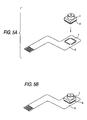
- FIGS. 5A and 5B show a method of mounting a camera module 1 on a flexible printed circuit (FPC) 6 .
- FPC flexible printed circuit
- terminals 7 of a printed circuit (not shown) are provided in an exposed manner on the flexible printed circuit 6 .
- the camera module 1 is placed on the terminals 7 , so that the terminals 4 of the camera module 1 are connected respectively to the terminals 7 by solder 8 as shown in FIG. 5 B.
- productivity is low, and camera placement accuracy is poor.
- a mounting method comprising steps of:
- the soldering step is performed in a non-manual manner.
- the soldering step is performed with a reflowing process.
- the wiring board is a printed wiring board.
- the wiring board is a flexible printed board.
- the camera module is detachably mounted on the connector.
- the camera module can be easily exchanged when the camera module is found to be defective.
- FIG. 1 is a perspective view showing a mounting method of a camera module according to a first embodiment of the invention
- FIGS. 2A to 2 D are perspective views showing each process of the mounting method
- FIG. 3 is a perspective view showing a mounting method of a camera module according to a second embodiment of the invention.
- FIGS. 4A and 4B are perspective views showing a first related-art method of a camera module.
- FIGS. 5A and 5B are perspective views showing a second related-art method of a camera module.
- FIG. 1 shows a method of mounting a camera module 11 on a printed wiring board 12 .
- Terminals 13 of a printed circuit (not shown) are provided in an exposed manner on the printed wiring board 12 , and a connector 14 is fixedly secured onto the terminals 13 by soldering.
- the camera module 11 is then fitted into the connector 14 , thereby mounting the camera module 11 on the printed wiring board 12 .
- FIGS. 2A to 2 D show each process of mounting the camera module 11 on the printed wiring board 12 .
- solder 15 is placed on the exposed terminals 13 provided on the printed wiring board 12 .
- the connector 14 is placed on the terminals 13 through the solder 15 , and the automatic mounting of this connector is performed with a reflowing process as shown in FIG. 2 B.
- FIG. 2C the camera module 11 is fitted into the connector 14 , so that the camera module 11 is mounted on the printed wiring board 12 as shown in FIG. 2 D.
- the camera module 11 is mounted on the printed wiring board 12 through the connector 14 , the automatic mounting using the reflowing process can be adopted when mounting the connector 14 on the printed wiring board 12 . Therefore, as compared with the manual mounting, the working efficiency can be greatly enhanced, and besides the mounting precision can be enhanced.
- the camera module 11 is detachably fitted into the connector 14 , if the camera module 11 is found to be defective in an inspection process or the like, this camera module can be easily exchanged.
- FIG. 3 shows a method of mounting a camera module 11 on a flexible printed circuit 16 .
- solder 18 is first placed on terminals 17 of a not-shown printed circuit provided in an exposed manner on the flexible printed circuit 16 .
- the connector 14 is then placed on the terminals 17 through the solder 18 , and the automatic mounting of this connector is performed with the reflowing process.
- the camera module 11 is fitted into the connector 14 , thereby mounting the camera module 11 on the flexible printed circuit 16 .
- the flexible printed circuit 16 has sufficient heat-resistance to withstand the reflowing process.
- the mounting method of the invention can be used for mounting, another parts or module such as a Bluetooth module, instead of the camera module.
Landscapes
- Engineering & Computer Science (AREA)
- Multimedia (AREA)
- Signal Processing (AREA)
- Manufacturing & Machinery (AREA)
- Microelectronics & Electronic Packaging (AREA)
- Structures For Mounting Electric Components On Printed Circuit Boards (AREA)
- Studio Devices (AREA)
- Electric Connection Of Electric Components To Printed Circuits (AREA)
- Combinations Of Printed Boards (AREA)
Abstract
Description
Claims (7)
Applications Claiming Priority (2)
| Application Number | Priority Date | Filing Date | Title |
|---|---|---|---|
| JP2002220085A JP3755149B2 (en) | 2002-07-29 | 2002-07-29 | Mounting the camera module on the board |
| JPP.2002-220085 | 2002-07-29 |
Publications (2)
| Publication Number | Publication Date |
|---|---|
| US20040068868A1 US20040068868A1 (en) | 2004-04-15 |
| US6862804B2 true US6862804B2 (en) | 2005-03-08 |
Family
ID=30112902
Family Applications (1)
| Application Number | Title | Priority Date | Filing Date |
|---|---|---|---|
| US10/627,918 Expired - Fee Related US6862804B2 (en) | 2002-07-29 | 2003-07-28 | Method of mounting camera module on wiring board |
Country Status (5)
| Country | Link |
|---|---|
| US (1) | US6862804B2 (en) |
| EP (1) | EP1387442B1 (en) |
| JP (1) | JP3755149B2 (en) |
| KR (1) | KR100798732B1 (en) |
| DE (1) | DE60330422D1 (en) |
Cited By (25)
| Publication number | Priority date | Publication date | Assignee | Title |
|---|---|---|---|---|
| US20050048829A1 (en) * | 2003-08-27 | 2005-03-03 | Atsushi Nishio | Connector for camera module use |
| US20060014405A1 (en) * | 2004-07-13 | 2006-01-19 | Research In Motion Limited | Structure for mounting a component to a circuit-board |
| US20060189183A1 (en) * | 2005-02-18 | 2006-08-24 | Ming-Hsun Yang | Camera module connector |
| US20060189216A1 (en) * | 2005-02-18 | 2006-08-24 | Ming-Hsun Yang | Camera module connector keying structure |
| US7121864B1 (en) * | 2005-09-30 | 2006-10-17 | Hon Hai Precision Ind. Co., Ltd. | Module connector |
| US20060258218A1 (en) * | 2005-05-16 | 2006-11-16 | Hon Hai Precision Ind. Co., Ltd. | Electrical connector with improved terminals |
| US20070037448A1 (en) * | 2005-08-11 | 2007-02-15 | Hon Hai Precision Ind. Co., Ltd. | Module assembly and equipment for fitting the same |
| US20070077823A1 (en) * | 2005-10-03 | 2007-04-05 | Hon Hai Precision Ind. Co., Ltd. | Shielded electrical connector for camera module |
| US20070232143A1 (en) * | 2006-04-03 | 2007-10-04 | Hon Hai Precision Ind. Co. Ltd. | Electrical connector having improved shield |
| US20080008468A1 (en) * | 2006-07-04 | 2008-01-10 | Hon Hai Precision Ind. Co., Ltd. | Camera module |
| US20080032553A1 (en) * | 2006-08-01 | 2008-02-07 | Hon Hai Precision Ind. Co., Ltd. | Electrical connector having improved shield |
| US20080119080A1 (en) * | 2006-11-17 | 2008-05-22 | Molex Incorporated | Zoom lens camera module socket |
| US20080194122A1 (en) * | 2005-01-31 | 2008-08-14 | Molex Incorporated | Socket for Camera Module |
| US20080267617A1 (en) * | 2007-04-27 | 2008-10-30 | Hon Hai Precision Industry Co., Ltd. | Electrical connector and camera device having the same |
| CN100435430C (en) * | 2005-07-21 | 2008-11-19 | Smk株式会社 | Receptacle for mounting electronic components and contact holder used therefor |
| US20090225441A1 (en) * | 2007-03-08 | 2009-09-10 | Satoshi Do | Imaging lens |
| US20090279188A1 (en) * | 2006-12-07 | 2009-11-12 | Satoshi Do | Imaging Lens |
| US20090290235A1 (en) * | 2006-12-21 | 2009-11-26 | Milestone Co., Ltd. | Imaging lens |
| US20100118416A1 (en) * | 2007-05-17 | 2010-05-13 | Satoshi Do | Imaging lens |
| US20100165485A1 (en) * | 2007-05-09 | 2010-07-01 | Mr. Satoshi Do | Imaging lens |
| US20100165486A1 (en) * | 2007-05-17 | 2010-07-01 | Satoshi Do | Imaging Lens |
| US8023202B2 (en) * | 2007-05-17 | 2011-09-20 | Milestone Co., Ltd. | Imaging lens |
| US8958212B2 (en) | 2011-01-05 | 2015-02-17 | Asustek Computer Inc. | Electronic device |
| USD817880S1 (en) * | 2016-03-01 | 2018-05-15 | Smk Corporation | Electrical connector |
| USD817881S1 (en) * | 2016-03-01 | 2018-05-15 | Smk Corporation | Electrical connector |
Families Citing this family (16)
| Publication number | Priority date | Publication date | Assignee | Title |
|---|---|---|---|---|
| JP2005222876A (en) | 2004-02-09 | 2005-08-18 | Smk Corp | Module connector |
| TWI282873B (en) * | 2004-03-12 | 2007-06-21 | Premier Image Technology Corp | Lens module and assembling method thereof |
| KR100568769B1 (en) | 2004-04-23 | 2006-04-07 | 앰코 테크놀로지 코리아 주식회사 | Mount for Camera Module |
| CN2749141Y (en) * | 2004-10-25 | 2005-12-28 | 富士康(昆山)电脑接插件有限公司 | Electric connector |
| JP4091593B2 (en) * | 2004-11-05 | 2008-05-28 | Smk株式会社 | Connection structure of camera module with autofocus function and module connector |
| CN2766377Y (en) * | 2004-12-04 | 2006-03-22 | 富士康(昆山)电脑接插件有限公司 | Electric connector |
| CN2791967Y (en) * | 2005-03-25 | 2006-06-28 | 富士康(昆山)电脑接插件有限公司 | Electric connector |
| CN100377434C (en) * | 2005-08-05 | 2008-03-26 | 富士康(昆山)电脑接插件有限公司 | Electrical Connector Assembly |
| KR101110152B1 (en) * | 2006-01-06 | 2012-01-31 | 에스케이플래닛 주식회사 | Remote aquarium viewing system and method using mobile communication terminal |
| KR100772601B1 (en) * | 2006-06-14 | 2007-11-01 | 서울전자통신(주) | Camera Module Installation Method |
| JP2009017234A (en) * | 2007-07-04 | 2009-01-22 | Sharp Corp | Camera device |
| KR101594831B1 (en) | 2009-03-26 | 2016-02-17 | 삼성전자 주식회사 | Camera module fixing structure in bio drive |
| KR20110002266A (en) * | 2009-07-01 | 2011-01-07 | 삼성테크윈 주식회사 | Imaging module |
| DE102010023293B4 (en) | 2010-06-10 | 2023-04-27 | HELLA GmbH & Co. KGaA | Camera for a motor vehicle |
| KR102375465B1 (en) | 2015-05-22 | 2022-03-21 | 주식회사 탑 엔지니어링 | Apparatus for mounting camera module |
| JP6390664B2 (en) * | 2016-05-20 | 2018-09-19 | Smk株式会社 | Optical electronic component and socket connection structure |
Citations (10)
| Publication number | Priority date | Publication date | Assignee | Title |
|---|---|---|---|---|
| US5046953A (en) * | 1990-05-25 | 1991-09-10 | Hewlett-Packard Company | Method and apparatus for mounting an integrated circuit on a printed circuit board |
| US5046954A (en) | 1991-01-31 | 1991-09-10 | Amp Incorporated | Planar electrical connector |
| US5302778A (en) * | 1992-08-28 | 1994-04-12 | Eastman Kodak Company | Semiconductor insulation for optical devices |
| US5358412A (en) * | 1993-04-26 | 1994-10-25 | Eastman Kodak Company | Method and apparatus for assembling a flexible circuit to an LCD module |
| US5847887A (en) * | 1995-02-28 | 1998-12-08 | Ohtsuka Patent Office | Optical apparatus |
| US20010027873A1 (en) | 2000-04-10 | 2001-10-11 | Mitsubishi Denki Kabushiki Kaisha | Image pickup device and portable telephone |
| EP1148716A1 (en) | 2000-04-07 | 2001-10-24 | Mitsubishi Denki Kabushiki Kaisha | Imaging device |
| US20010055073A1 (en) | 2000-06-16 | 2001-12-27 | Kohji Shinomiya | Solid state imaging apparatus |
| EP1213924A1 (en) | 2000-11-30 | 2002-06-12 | Mitsubishi Denki Kabushiki Kaisha | Portable telephone provided with image pickup device |
| US6470103B2 (en) * | 1998-03-20 | 2002-10-22 | Fujitsu Limited | Semiconductor parts and semiconductor mounting apparatus |
-
2002
- 2002-07-29 JP JP2002220085A patent/JP3755149B2/en not_active Expired - Fee Related
-
2003
- 2003-07-24 KR KR1020030050944A patent/KR100798732B1/en not_active Expired - Fee Related
- 2003-07-28 US US10/627,918 patent/US6862804B2/en not_active Expired - Fee Related
- 2003-07-29 EP EP03017204A patent/EP1387442B1/en not_active Expired - Lifetime
- 2003-07-29 DE DE60330422T patent/DE60330422D1/en not_active Expired - Lifetime
Patent Citations (12)
| Publication number | Priority date | Publication date | Assignee | Title |
|---|---|---|---|---|
| US5046953A (en) * | 1990-05-25 | 1991-09-10 | Hewlett-Packard Company | Method and apparatus for mounting an integrated circuit on a printed circuit board |
| US5046954A (en) | 1991-01-31 | 1991-09-10 | Amp Incorporated | Planar electrical connector |
| US5302778A (en) * | 1992-08-28 | 1994-04-12 | Eastman Kodak Company | Semiconductor insulation for optical devices |
| US5358412A (en) * | 1993-04-26 | 1994-10-25 | Eastman Kodak Company | Method and apparatus for assembling a flexible circuit to an LCD module |
| US5847887A (en) * | 1995-02-28 | 1998-12-08 | Ohtsuka Patent Office | Optical apparatus |
| US6470103B2 (en) * | 1998-03-20 | 2002-10-22 | Fujitsu Limited | Semiconductor parts and semiconductor mounting apparatus |
| US6566669B2 (en) * | 1998-03-20 | 2003-05-20 | Fujitsu Limited | Semiconductor parts and semiconductor mounting apparatus |
| US6583402B1 (en) * | 1998-03-20 | 2003-06-24 | Fujitsu Limited | Semiconductor parts and semiconductor mounting apparatus |
| EP1148716A1 (en) | 2000-04-07 | 2001-10-24 | Mitsubishi Denki Kabushiki Kaisha | Imaging device |
| US20010027873A1 (en) | 2000-04-10 | 2001-10-11 | Mitsubishi Denki Kabushiki Kaisha | Image pickup device and portable telephone |
| US20010055073A1 (en) | 2000-06-16 | 2001-12-27 | Kohji Shinomiya | Solid state imaging apparatus |
| EP1213924A1 (en) | 2000-11-30 | 2002-06-12 | Mitsubishi Denki Kabushiki Kaisha | Portable telephone provided with image pickup device |
Cited By (40)
| Publication number | Priority date | Publication date | Assignee | Title |
|---|---|---|---|---|
| US7112083B2 (en) * | 2003-08-27 | 2006-09-26 | Mitsumi Electric Co., Ltd. | Connector for camera module use |
| US20050048829A1 (en) * | 2003-08-27 | 2005-03-03 | Atsushi Nishio | Connector for camera module use |
| US7918671B2 (en) * | 2004-07-13 | 2011-04-05 | Research In Motion Limited | Mounting structure with springs biasing towards a latching edge |
| US20060014405A1 (en) * | 2004-07-13 | 2006-01-19 | Research In Motion Limited | Structure for mounting a component to a circuit-board |
| US7699619B2 (en) | 2005-01-31 | 2010-04-20 | Molex Incorporated | Socket for camera module |
| US20080194122A1 (en) * | 2005-01-31 | 2008-08-14 | Molex Incorporated | Socket for Camera Module |
| US20060189216A1 (en) * | 2005-02-18 | 2006-08-24 | Ming-Hsun Yang | Camera module connector keying structure |
| US20060189183A1 (en) * | 2005-02-18 | 2006-08-24 | Ming-Hsun Yang | Camera module connector |
| US7179126B2 (en) * | 2005-05-16 | 2007-02-20 | Hon Hai Precision Ind. Co., Ltd. | Electrical connector with improved terminals |
| US20060258218A1 (en) * | 2005-05-16 | 2006-11-16 | Hon Hai Precision Ind. Co., Ltd. | Electrical connector with improved terminals |
| CN100435430C (en) * | 2005-07-21 | 2008-11-19 | Smk株式会社 | Receptacle for mounting electronic components and contact holder used therefor |
| US20070037448A1 (en) * | 2005-08-11 | 2007-02-15 | Hon Hai Precision Ind. Co., Ltd. | Module assembly and equipment for fitting the same |
| US7255600B2 (en) | 2005-08-11 | 2007-08-14 | Hon Hai Precision Ind. Co., Ltd. | Module assembly and equipment for fitting the same |
| US7121864B1 (en) * | 2005-09-30 | 2006-10-17 | Hon Hai Precision Ind. Co., Ltd. | Module connector |
| US7241160B2 (en) | 2005-10-03 | 2007-07-10 | Hon Hai Precision Ind. Co., Ltd | Shielded electrical connector for camera module |
| US20070077823A1 (en) * | 2005-10-03 | 2007-04-05 | Hon Hai Precision Ind. Co., Ltd. | Shielded electrical connector for camera module |
| US20070232143A1 (en) * | 2006-04-03 | 2007-10-04 | Hon Hai Precision Ind. Co. Ltd. | Electrical connector having improved shield |
| US7435139B2 (en) * | 2006-04-03 | 2008-10-14 | Hon Hai Precision Ind. Co., Ltd. | Electrical connector having improved shield |
| US20080008468A1 (en) * | 2006-07-04 | 2008-01-10 | Hon Hai Precision Ind. Co., Ltd. | Camera module |
| US20080032553A1 (en) * | 2006-08-01 | 2008-02-07 | Hon Hai Precision Ind. Co., Ltd. | Electrical connector having improved shield |
| US7422482B2 (en) * | 2006-08-01 | 2008-09-09 | Hon Hai Precision Inc. Co., Ltd. | Electrical connector having improved shield |
| US20080119080A1 (en) * | 2006-11-17 | 2008-05-22 | Molex Incorporated | Zoom lens camera module socket |
| US8149525B2 (en) | 2006-12-07 | 2012-04-03 | Satoshi Do | Imaging lens |
| US20090279188A1 (en) * | 2006-12-07 | 2009-11-12 | Satoshi Do | Imaging Lens |
| US20090290235A1 (en) * | 2006-12-21 | 2009-11-26 | Milestone Co., Ltd. | Imaging lens |
| US7768720B2 (en) | 2006-12-21 | 2010-08-03 | Satoshi Do | Imaging lens |
| US20090225441A1 (en) * | 2007-03-08 | 2009-09-10 | Satoshi Do | Imaging lens |
| US7656593B2 (en) | 2007-03-08 | 2010-02-02 | Satoshi Do | Imaging lens |
| US7682159B2 (en) * | 2007-04-27 | 2010-03-23 | Hon Hai Precision Industry Co., Ltd. | Electrical connector and camera device having the same |
| US20080267617A1 (en) * | 2007-04-27 | 2008-10-30 | Hon Hai Precision Industry Co., Ltd. | Electrical connector and camera device having the same |
| US7880981B2 (en) | 2007-05-09 | 2011-02-01 | Satoshi Do | Imaging lens |
| US20100165485A1 (en) * | 2007-05-09 | 2010-07-01 | Mr. Satoshi Do | Imaging lens |
| US20100165486A1 (en) * | 2007-05-17 | 2010-07-01 | Satoshi Do | Imaging Lens |
| US20100118416A1 (en) * | 2007-05-17 | 2010-05-13 | Satoshi Do | Imaging lens |
| US7830619B2 (en) | 2007-05-17 | 2010-11-09 | Satoshi Do | Imaging lens |
| US8014083B2 (en) | 2007-05-17 | 2011-09-06 | Satoshi Do | Imaging lens |
| US8023202B2 (en) * | 2007-05-17 | 2011-09-20 | Milestone Co., Ltd. | Imaging lens |
| US8958212B2 (en) | 2011-01-05 | 2015-02-17 | Asustek Computer Inc. | Electronic device |
| USD817880S1 (en) * | 2016-03-01 | 2018-05-15 | Smk Corporation | Electrical connector |
| USD817881S1 (en) * | 2016-03-01 | 2018-05-15 | Smk Corporation | Electrical connector |
Also Published As
| Publication number | Publication date |
|---|---|
| EP1387442A1 (en) | 2004-02-04 |
| KR20040011360A (en) | 2004-02-05 |
| EP1387442B1 (en) | 2009-12-09 |
| JP2004063787A (en) | 2004-02-26 |
| DE60330422D1 (en) | 2010-01-21 |
| KR100798732B1 (en) | 2008-01-29 |
| US20040068868A1 (en) | 2004-04-15 |
| JP3755149B2 (en) | 2006-03-15 |
Similar Documents
| Publication | Publication Date | Title |
|---|---|---|
| US6862804B2 (en) | Method of mounting camera module on wiring board | |
| JP2850860B2 (en) | Electronic component manufacturing method | |
| US12219712B2 (en) | Printed circuit board and electronic device | |
| US20020093803A1 (en) | Adapter for plastic-leaded chip carrier (PLCC) and other surface mount technology (SMT) chip carriers | |
| US20040121632A1 (en) | Connector mounting structure and connector mounting method | |
| US20120051017A1 (en) | Electronic Component and Method of Manufacturing the Same | |
| US6881906B2 (en) | Printed circuit board comprising a contact sleeve that is mounted thereon | |
| JPH09326269A (en) | SMT connector | |
| JPH0745346A (en) | Socket for chip part | |
| JP3799615B2 (en) | Mounting the camera module on the board | |
| JP2606103Y2 (en) | Jack connector device | |
| NO995380L (en) | Electrical circuit board component and method for automatic mounting of circuit boards with such components | |
| EP1377142A3 (en) | Method of producing electronic unit of radio system automatically, electronic unit of radio system and electronic component used for its production | |
| EP1416778A3 (en) | Small and securely-soldered electronic unit | |
| RU2363070C2 (en) | Independent electronic component and method of its mounting | |
| KR100538145B1 (en) | Module with different boards and method for assembly the module | |
| US20150016069A1 (en) | Printed circuit board | |
| TWI265758B (en) | Electronic component mounting method, substrate manufacturing apparatus, and circuit board | |
| CN101005170A (en) | Plate-to-plate connection structure | |
| JP2003187890A (en) | Electrical connection terminal | |
| EP1399006A2 (en) | A mounting structure of a wireless module | |
| KR200408838Y1 (en) | Printed circuit board | |
| US20060213058A1 (en) | Circuit board for surface-mount device to be mounted thereon | |
| JPH09298351A (en) | Circuit pattern converting subprinted board | |
| JP3101815U (en) | PCB mounting structure |
Legal Events
| Date | Code | Title | Description |
|---|---|---|---|
| AS | Assignment |
Owner name: MITSUMI ELECTRIC CO., LTD., JAPAN Free format text: ASSIGNMENT OF ASSIGNORS INTEREST;ASSIGNORS:NISHIO, ATSUSHI;KAWASAKI, TAKASHI;REEL/FRAME:014356/0620 Effective date: 20030723 |
|
| FPAY | Fee payment |
Year of fee payment: 4 |
|
| FPAY | Fee payment |
Year of fee payment: 8 |
|
| REMI | Maintenance fee reminder mailed | ||
| LAPS | Lapse for failure to pay maintenance fees | ||
| STCH | Information on status: patent discontinuation |
Free format text: PATENT EXPIRED DUE TO NONPAYMENT OF MAINTENANCE FEES UNDER 37 CFR 1.362 |
|
| STCH | Information on status: patent discontinuation |
Free format text: PATENT EXPIRED DUE TO NONPAYMENT OF MAINTENANCE FEES UNDER 37 CFR 1.362 |
|
| FP | Lapsed due to failure to pay maintenance fee |
Effective date: 20170308 |