EP1387442B1 - Method of mounting camera module on wiring board - Google Patents
Method of mounting camera module on wiring board Download PDFInfo
- Publication number
- EP1387442B1 EP1387442B1 EP03017204A EP03017204A EP1387442B1 EP 1387442 B1 EP1387442 B1 EP 1387442B1 EP 03017204 A EP03017204 A EP 03017204A EP 03017204 A EP03017204 A EP 03017204A EP 1387442 B1 EP1387442 B1 EP 1387442B1
- Authority
- EP
- European Patent Office
- Prior art keywords
- camera module
- wiring board
- terminal
- mounting
- connector
- Prior art date
- Legal status (The legal status is an assumption and is not a legal conclusion. Google has not performed a legal analysis and makes no representation as to the accuracy of the status listed.)
- Expired - Fee Related
Links
Images


Classifications
-
- H—ELECTRICITY
- H01—ELECTRIC ELEMENTS
- H01R—ELECTRICALLY-CONDUCTIVE CONNECTIONS; STRUCTURAL ASSOCIATIONS OF A PLURALITY OF MUTUALLY-INSULATED ELECTRICAL CONNECTING ELEMENTS; COUPLING DEVICES; CURRENT COLLECTORS
- H01R12/00—Structural associations of a plurality of mutually-insulated electrical connecting elements, specially adapted for printed circuits, e.g. printed circuit boards [PCB], flat or ribbon cables, or like generally planar structures, e.g. terminal strips, terminal blocks; Coupling devices specially adapted for printed circuits, flat or ribbon cables, or like generally planar structures; Terminals specially adapted for contact with, or insertion into, printed circuits, flat or ribbon cables, or like generally planar structures
- H01R12/70—Coupling devices
- H01R12/7076—Coupling devices for connection between PCB and component, e.g. display
-
- H—ELECTRICITY
- H04—ELECTRIC COMMUNICATION TECHNIQUE
- H04N—PICTORIAL COMMUNICATION, e.g. TELEVISION
- H04N23/00—Cameras or camera modules comprising electronic image sensors; Control thereof
- H04N23/50—Constructional details
- H04N23/54—Mounting of pick-up tubes, electronic image sensors, deviation or focusing coils
-
- H—ELECTRICITY
- H05—ELECTRIC TECHNIQUES NOT OTHERWISE PROVIDED FOR
- H05K—PRINTED CIRCUITS; CASINGS OR CONSTRUCTIONAL DETAILS OF ELECTRIC APPARATUS; MANUFACTURE OF ASSEMBLAGES OF ELECTRICAL COMPONENTS
- H05K3/00—Apparatus or processes for manufacturing printed circuits
- H05K3/30—Assembling printed circuits with electric components, e.g. with resistor
- H05K3/301—Assembling printed circuits with electric components, e.g. with resistor by means of a mounting structure
-
- Y—GENERAL TAGGING OF NEW TECHNOLOGICAL DEVELOPMENTS; GENERAL TAGGING OF CROSS-SECTIONAL TECHNOLOGIES SPANNING OVER SEVERAL SECTIONS OF THE IPC; TECHNICAL SUBJECTS COVERED BY FORMER USPC CROSS-REFERENCE ART COLLECTIONS [XRACs] AND DIGESTS
- Y10—TECHNICAL SUBJECTS COVERED BY FORMER USPC
- Y10T—TECHNICAL SUBJECTS COVERED BY FORMER US CLASSIFICATION
- Y10T29/00—Metal working
- Y10T29/49—Method of mechanical manufacture
- Y10T29/49002—Electrical device making
- Y10T29/49117—Conductor or circuit manufacturing
- Y10T29/49124—On flat or curved insulated base, e.g., printed circuit, etc.
- Y10T29/4913—Assembling to base an electrical component, e.g., capacitor, etc.
- Y10T29/49131—Assembling to base an electrical component, e.g., capacitor, etc. by utilizing optical sighting device
-
- Y—GENERAL TAGGING OF NEW TECHNOLOGICAL DEVELOPMENTS; GENERAL TAGGING OF CROSS-SECTIONAL TECHNOLOGIES SPANNING OVER SEVERAL SECTIONS OF THE IPC; TECHNICAL SUBJECTS COVERED BY FORMER USPC CROSS-REFERENCE ART COLLECTIONS [XRACs] AND DIGESTS
- Y10—TECHNICAL SUBJECTS COVERED BY FORMER USPC
- Y10T—TECHNICAL SUBJECTS COVERED BY FORMER US CLASSIFICATION
- Y10T29/00—Metal working
- Y10T29/49—Method of mechanical manufacture
- Y10T29/49002—Electrical device making
- Y10T29/49117—Conductor or circuit manufacturing
- Y10T29/49124—On flat or curved insulated base, e.g., printed circuit, etc.
- Y10T29/4913—Assembling to base an electrical component, e.g., capacitor, etc.
- Y10T29/49133—Assembling to base an electrical component, e.g., capacitor, etc. with component orienting
-
- Y—GENERAL TAGGING OF NEW TECHNOLOGICAL DEVELOPMENTS; GENERAL TAGGING OF CROSS-SECTIONAL TECHNOLOGIES SPANNING OVER SEVERAL SECTIONS OF THE IPC; TECHNICAL SUBJECTS COVERED BY FORMER USPC CROSS-REFERENCE ART COLLECTIONS [XRACs] AND DIGESTS
- Y10—TECHNICAL SUBJECTS COVERED BY FORMER USPC
- Y10T—TECHNICAL SUBJECTS COVERED BY FORMER US CLASSIFICATION
- Y10T29/00—Metal working
- Y10T29/49—Method of mechanical manufacture
- Y10T29/49002—Electrical device making
- Y10T29/49117—Conductor or circuit manufacturing
- Y10T29/49124—On flat or curved insulated base, e.g., printed circuit, etc.
- Y10T29/4913—Assembling to base an electrical component, e.g., capacitor, etc.
- Y10T29/49144—Assembling to base an electrical component, e.g., capacitor, etc. by metal fusion
-
- Y—GENERAL TAGGING OF NEW TECHNOLOGICAL DEVELOPMENTS; GENERAL TAGGING OF CROSS-SECTIONAL TECHNOLOGIES SPANNING OVER SEVERAL SECTIONS OF THE IPC; TECHNICAL SUBJECTS COVERED BY FORMER USPC CROSS-REFERENCE ART COLLECTIONS [XRACs] AND DIGESTS
- Y10—TECHNICAL SUBJECTS COVERED BY FORMER USPC
- Y10T—TECHNICAL SUBJECTS COVERED BY FORMER US CLASSIFICATION
- Y10T29/00—Metal working
- Y10T29/49—Method of mechanical manufacture
- Y10T29/49002—Electrical device making
- Y10T29/49117—Conductor or circuit manufacturing
- Y10T29/49124—On flat or curved insulated base, e.g., printed circuit, etc.
- Y10T29/49147—Assembling terminal to base
- Y10T29/49149—Assembling terminal to base by metal fusion bonding
-
- Y—GENERAL TAGGING OF NEW TECHNOLOGICAL DEVELOPMENTS; GENERAL TAGGING OF CROSS-SECTIONAL TECHNOLOGIES SPANNING OVER SEVERAL SECTIONS OF THE IPC; TECHNICAL SUBJECTS COVERED BY FORMER USPC CROSS-REFERENCE ART COLLECTIONS [XRACs] AND DIGESTS
- Y10—TECHNICAL SUBJECTS COVERED BY FORMER USPC
- Y10T—TECHNICAL SUBJECTS COVERED BY FORMER US CLASSIFICATION
- Y10T29/00—Metal working
- Y10T29/49—Method of mechanical manufacture
- Y10T29/49002—Electrical device making
- Y10T29/49117—Conductor or circuit manufacturing
- Y10T29/49169—Assembling electrical component directly to terminal or elongated conductor
-
- Y—GENERAL TAGGING OF NEW TECHNOLOGICAL DEVELOPMENTS; GENERAL TAGGING OF CROSS-SECTIONAL TECHNOLOGIES SPANNING OVER SEVERAL SECTIONS OF THE IPC; TECHNICAL SUBJECTS COVERED BY FORMER USPC CROSS-REFERENCE ART COLLECTIONS [XRACs] AND DIGESTS
- Y10—TECHNICAL SUBJECTS COVERED BY FORMER USPC
- Y10T—TECHNICAL SUBJECTS COVERED BY FORMER US CLASSIFICATION
- Y10T29/00—Metal working
- Y10T29/53—Means to assemble or disassemble
- Y10T29/5313—Means to assemble electrical device
- Y10T29/53174—Means to fasten electrical component to wiring board, base, or substrate
- Y10T29/53178—Chip component
Definitions
- the invention relates to a mounting method for a camera module (particularly provided with a cellular phone) on a wiring board (circuit board).
- EP 1148 716 A discloses a mounting method for a camera module comprising the steps of providing a wiring board provided with a first terminal; providing a connector having a space surrounded by four joined side walls and provided with a second terminal; providing a camera module provided with a third terminal; soldering the first terminal and the second terminal and mounting the camera module on the connector.
- US 2001/055073 A1 discloses a solid state imaging apparatus.
- Said apparatus comprises a solid state Imaging element an optical lens held by a frame, and a flexible printed circuit board having two surfaces.
- the solid state imaging element Is mounted on one surface of the flexible printed circuit board and the frame Is mounted on the other surface.
- EP 1 065 751 A refers to the mounting of electronic components on circuit boards.
- the circuit board has a hole that is large enough to accommodate a portion of an electronic component Contacts are arranged along a side wall of the accommodated portion of the component Other contacts are mounted on the board and exposed along the periphery of the hole.
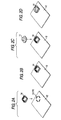
- Figs. 4A and 4B show method of mounting a camera module 1 an a printed wiring board (PWB) 2.
- PWB printed wiring board
- terminals 8 of a printed circuit (not shown) are provided in an exposed manner on the printed wiring board 2.
- the camera module 1 is placed on the terminals 3, so that terminals 4 of the camera module 1 are connected respectively to the terminals a by solder 5 as shown in Fig. 4B .
- the camera module 1 Since the camera module 1 is not sufficiently heat-resistant to withstand a furnace temperature of about 230 to 240°C used in a reflowing process, it is impossible to perform the soldering with the reflowing process Therefore, the mounting operation of the camera module 1 is manually executed with a manual soldering
- Fig. 5A and 5B show a method of mounting a camera module 1 on a flexible printed circuit (FPC) 6.
- FPC flexible printed circuit
- terminals 7 of a printed circuit (not shown are provided in an exposed manner an the flexible printed circuit 6.
- the camera module 1 is placed on the terminals 7, so that the terminals 4 of the camera module 1 are connected respectively to the terminals 7 by solder 8 as shown in Fig. 5B .
- a mounting method for a camera module comprising the steps of:
- the soldering step is performed in a non-manual manner.
- the soldering step is performed with a reflowing process.
- the wiring board is a printed wiring board
- the wiring board is flexible printed aboard.
- the camera module is detachably mounted on the connector.
- the camera module can be easily exchanged when the camera module is found to be defective,.
- Fig. 1 shows a method of mounting a camera module 11 on a printed wiring board 12.
- Terminals 13 of a printed circuit (not shown) are provided in an exposed manner on the printed wiring board 12, and a connector 14 is fixedly secured onto the terminals 13 by soldering.
- the camera module 11 is then fitted into the connector 14, thereby mounting the camera module 11 on the printed wiring board 12.
- Figs. 2A to 2D show each process of mounting the camera module 11 on the printed wiring board 12.
- solder 15 is placed on the exposed terminals 13 provided on the printed wiring board 12.
- the connector 14 is placed on the terminals 13 through the solder 15, and the automatic mounting of this connector is performed with a reflowing process as shown in Fig. 2B .
- the camera module 11 is fitted into the connector 14, so that the camera module 11 is mounted on the printed wiring board 12 as shown in Fig. 2D .
- the automatic mounting using the reflowing process can be adopted when mounting the connector 14 on the printed wiring board 12. Therefore, as compared with the manual mounting, the working efficiency can be greatly enhanced, and besides the mounting precision can be enhanced.
- the camera module 11 is detachably fitted into the connector 14, if the camera module 11 is found to be defective in an inspection process or the like, this camera module can be easily exchanged.
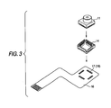
- Fig. 3 shows a method of mounting a camera module 11 on a flexible printed circuit 16.
- solder 18 is first placed on terminals 17 of a not-shown printed circuit provided in an exposed manner on the flexible printed circuit 16.
- the connector 14 is then placed on the terminals 17 through the solder 18, and the automatic mounting of this connector is performed with the reflowing process.
- the camera module 11 is fitted into the connector 14, thereby mounting the camera module 11 on the flexible printed circuit 16.
- the flexible printed circuit 16 has sufficient heat-reaiatance to withstand the reflowing process.
- the mounting method of the invention can be used for mounting, another parts or module such as a Bluetooth module, instead of the camera module.
Description
- The invention relates to a mounting method for a camera module (particularly provided with a cellular phone) on a wiring board (circuit board).
-
EP 1148 716 A discloses a mounting method for a camera module comprising the steps of providing a wiring board provided with a first terminal; providing a connector having a space surrounded by four joined side walls and provided with a second terminal; providing a camera module provided with a third terminal; soldering the first terminal and the second terminal and mounting the camera module on the connector. -
US 2001/055073 A1 discloses a solid state imaging apparatus. Said apparatus comprises a solid state Imaging element an optical lens held by a frame, and a flexible printed circuit board having two surfaces. The solid state imaging element Is mounted on one surface of the flexible printed circuit board and the frame Is mounted on the other surface. -
EP 1 065 751 A refers to the mounting of electronic components on circuit boards. The circuit board has a hole that is large enough to accommodate a portion of an electronic component Contacts are arranged along a side wall of the accommodated portion of the component Other contacts are mounted on the board and exposed along the periphery of the hole. - Examples or the related-art method of mounting a camara module on a wiring board will be described with reference to
Fig. 4A through 5B . -
Figs. 4A and 4B show method of mounting a camera module 1 an a printed wiring board (PWB) 2. As shown inFig. 4A .terminals 8 of a printed circuit (not shown) are provided in an exposed manner on the printed wiring board 2. The camera module 1 is placed on theterminals 3, so thatterminals 4 of the camera module 1 are connected respectively to the terminals a by solder 5 as shown inFig. 4B . - Since the camera module 1 is not sufficiently heat-resistant to withstand a furnace temperature of about 230 to 240°C used in a reflowing process, it is impossible to perform the soldering with the reflowing process Therefore, the mounting operation of the camera module 1 is manually executed with a manual soldering
-
Fig. 5A and 5B show a method of mounting a camera module 1 on a flexible printed circuit (FPC) 6. As shown inFig. 5A terminals 7 of a printed circuit (not shown are provided in an exposed manner an the flexible printedcircuit 6. The camera module 1 is placed on theterminals 7, so that theterminals 4 of the camera module 1 are connected respectively to theterminals 7 bysolder 8 as shown inFig. 5B . - Also in this case, since it is impossible to perform the reflowing process due to the same reason as described above the mounting operation is manually executed with the manual soldering
- Therefore, the working efficiency is extremely low, and besides there was an anxiety that the mounting precision is lowered.
- It is therefore an object of the invention to provide as method of mounting a camera module on a wiring board, in which the working effeciency and the mounting precision are enhanced
- In order to achieve the above object, according to the invention, there is provided a mounting method for a camera module, comprising the steps of:
- providing a wiring board provided with a first terminal;
- providing a connector having a space surrounded by four joined side walls and provided with a second terminal, a first end portion of which is projected from an inner face of one of the side walls into the space;
- providing a camera module provided with a third terminal;
- soldering the first terminal and a second end portion of the second terminal to mount the connector on the wiring board; and
- fitting the camera module into the space of the connector to electrically connect the second terminal with the third terminal, while deforming the first end portion of the second terminal towards the side wall.
- Preferably, the soldering step is performed in a non-manual manner. Here, it is further preferable that the soldering step is performed with a reflowing process.
- Preferably, the wiring board is a printed wiring board Here, it is further preferable that the wiring board is flexible printed aboard.
- With the above configuration, since the automatic mounting such as the reflowing process can be adopted in the soldering step, as compared with the manual soldering, the working efficiency can be greatly enhanced, and besides the mounting precision can be enhanced.
- Preferably, the camera module is detachably mounted on the connector.
- With such a configuration, the camera module can be easily exchanged when the camera module is found to be defective,.
- The above objects and advantages of the present invention will become more apparent by describing in detail preferred exemplary embodiments thereof with reference to the accompanying drawings, wherein:
-
Fig. 1 is a perspective view showing a mounting method of a camera module according to a first embodiment of the invention; -
Figs. 2A to 2D are perspective views showing each process the mounting method; -
Fig. 3 is a perspective view showing a mounting method of a camera module according to a second embodiment of the invention; -
Figs. 4A and 4B are perspective views showing a first related-art method of a camera module; and -
Figs. 5A and 5B are perspective views showing a second related-art method of a camera module. - As a first embodiment of the invention,
Fig. 1 shows a method of mounting acamera module 11 on a printedwiring board 12.Terminals 13 of a printed circuit (not shown) are provided in an exposed manner on the printedwiring board 12, and aconnector 14 is fixedly secured onto theterminals 13 by soldering. Thecamera module 11 is then fitted into theconnector 14, thereby mounting thecamera module 11 on the printedwiring board 12. -
Figs. 2A to 2D show each process of mounting thecamera module 11 on the printedwiring board 12. InFig. 2A ,solder 15 is placed on the exposedterminals 13 provided on the printedwiring board 12. Theconnector 14 is placed on theterminals 13 through thesolder 15, and the automatic mounting of this connector is performed with a reflowing process as shown inFig. 2B . Then, as shown inFig. 2C , thecamera module 11 is fitted into theconnector 14, so that thecamera module 11 is mounted on the printedwiring board 12 as shown inFig. 2D . - In this embodiment, since the
camera module 11 is mounted on the printedwiring board 12 through theconnector 14, the automatic mounting using the reflowing process can be adopted when mounting theconnector 14 on the printedwiring board 12. Therefore, as compared with the manual mounting, the working efficiency can be greatly enhanced, and besides the mounting precision can be enhanced. - In addition, since the
camera module 11 is detachably fitted into theconnector 14, if thecamera module 11 is found to be defective in an inspection process or the like, this camera module can be easily exchanged. - As a second embodiment of the invention,
Fig. 3 shows a method of mounting acamera module 11 on a flexible printedcircuit 16. In this embodiment,solder 18 is first placed onterminals 17 of a not-shown printed circuit provided in an exposed manner on the flexible printedcircuit 16. Theconnector 14 is then placed on theterminals 17 through thesolder 18, and the automatic mounting of this connector is performed with the reflowing process. Finally, thecamera module 11 is fitted into theconnector 14, thereby mounting thecamera module 11 on the flexible printedcircuit 16. The flexible printedcircuit 16 has sufficient heat-reaiatance to withstand the reflowing process. - Also in this embodiment, the same advantages as explained with the first embodiment can be attained.
- Although the above explanation has been made for the case of mounting a camera module, the mounting method of the invention can be used for mounting, another parts or module such as a Bluetooth module, instead of the camera module.
Claims (6)
- A mounting method for a camera module, comprising the steps of:providing a wiring board (12) provided with a first terminal (13);providing a connector (14) having a space surrounded by four joined side walls and provided with a second terminal, a first end portion of which is projected from an inner face of one of the side walls into the space;providing a camera module (11) provided with a third terminal;soldering the first terminal and a second end portion of the second terminal to mount the connector (14) on the wiring board; andfitting the camera module into the space of the connector (14) to electrically connect the second terminal with the third terminal, while deforming the first end portion of the second terminal towards the side wall.
- The mounting method as set forth in claim 1, wherein the soldering step is performed in a non-manual manner.
- The mounting method as set forth in claim 2, wherein the soldering step is performed with a reflowing process.
- The mounting method as set forth in claim 1, wherein the wiring board is a printed wiring board (12).
- The mounting method as set forth in claim 1, wherein the wiring board is a flexible printed board (16).
- The mounting method as set forth in claim 1, wherein the camera module (11) is detachably mounted on the connector (14).
Applications Claiming Priority (2)
| Application Number | Priority Date | Filing Date | Title |
|---|---|---|---|
| JP2002220085A JP3755149B2 (en) | 2002-07-29 | 2002-07-29 | Mounting the camera module on the board |
| JP2002220085 | 2002-07-29 |
Publications (2)
| Publication Number | Publication Date |
|---|---|
| EP1387442A1 EP1387442A1 (en) | 2004-02-04 |
| EP1387442B1 true EP1387442B1 (en) | 2009-12-09 |
Family
ID=30112902
Family Applications (1)
| Application Number | Title | Priority Date | Filing Date |
|---|---|---|---|
| EP03017204A Expired - Fee Related EP1387442B1 (en) | 2002-07-29 | 2003-07-29 | Method of mounting camera module on wiring board |
Country Status (5)
| Country | Link |
|---|---|
| US (1) | US6862804B2 (en) |
| EP (1) | EP1387442B1 (en) |
| JP (1) | JP3755149B2 (en) |
| KR (1) | KR100798732B1 (en) |
| DE (1) | DE60330422D1 (en) |
Families Citing this family (41)
| Publication number | Priority date | Publication date | Assignee | Title |
|---|---|---|---|---|
| TW200509480A (en) * | 2003-08-27 | 2005-03-01 | Mitsumi Electric Co Ltd | Connector for camera module |
| JP2005222876A (en) | 2004-02-09 | 2005-08-18 | Smk Corp | Connector for module |
| TWI282873B (en) * | 2004-03-12 | 2007-06-21 | Premier Image Technology Corp | Lens module and assembling method thereof |
| KR100568769B1 (en) | 2004-04-23 | 2006-04-07 | 앰코 테크놀로지 코리아 주식회사 | Mount for Camera Module |
| US7918671B2 (en) * | 2004-07-13 | 2011-04-05 | Research In Motion Limited | Mounting structure with springs biasing towards a latching edge |
| CN2749141Y (en) * | 2004-10-25 | 2005-12-28 | 富士康(昆山)电脑接插件有限公司 | Electric connector |
| JP4091593B2 (en) * | 2004-11-05 | 2008-05-28 | Smk株式会社 | Connection structure of camera module with autofocus function and module connector |
| CN2766377Y (en) * | 2004-12-04 | 2006-03-22 | 富士康(昆山)电脑接插件有限公司 | Electric connector |
| JP4562538B2 (en) * | 2005-01-31 | 2010-10-13 | モレックス インコーポレイテド | Module socket |
| TWM271287U (en) * | 2005-02-18 | 2005-07-21 | Molex Taiwan Ltd | Camera module connector |
| US20060189216A1 (en) * | 2005-02-18 | 2006-08-24 | Ming-Hsun Yang | Camera module connector keying structure |
| CN2791967Y (en) * | 2005-03-25 | 2006-06-28 | 富士康(昆山)电脑接插件有限公司 | Electric connector |
| CN100399637C (en) * | 2005-05-16 | 2008-07-02 | 富士康(昆山)电脑接插件有限公司 | Electric connector |
| JP4182529B2 (en) * | 2005-07-21 | 2008-11-19 | Smk株式会社 | Electronic component mounting socket and contact carrier used therefor |
| CN100377434C (en) * | 2005-08-05 | 2008-03-26 | 富士康(昆山)电脑接插件有限公司 | Electric connector components |
| CN2831478Y (en) * | 2005-08-11 | 2006-10-25 | 富士康(昆山)电脑接插件有限公司 | Electrical connector assembly and electronic appliance installed the same |
| US7121864B1 (en) | 2005-09-30 | 2006-10-17 | Hon Hai Precision Ind. Co., Ltd. | Module connector |
| TWM288979U (en) * | 2005-10-03 | 2006-03-21 | Hon Hai Prec Ind Co Ltd | Electrical connector |
| KR101110152B1 (en) * | 2006-01-06 | 2012-01-31 | 에스케이플래닛 주식회사 | Remote aquarium viewing system and method using a mobile communication terminal |
| TWM304793U (en) * | 2006-04-03 | 2007-01-11 | Hon Hai Prec Ind Co Ltd | Electrical connector assembly |
| KR100772601B1 (en) * | 2006-06-14 | 2007-11-01 | 서울전자통신(주) | Method for mounting a camera module |
| CN2932759Y (en) * | 2006-07-04 | 2007-08-08 | 富士康(昆山)电脑接插件有限公司 | Electric connector assembly |
| CN200941518Y (en) * | 2006-08-01 | 2007-08-29 | 富士康(昆山)电脑接插件有限公司 | Electrical connector |
| TWM310502U (en) * | 2006-11-17 | 2007-04-21 | Molex Taiwan Ltd | Electrical connection device |
| JP3926380B1 (en) | 2006-12-07 | 2007-06-06 | マイルストーン株式会社 | Imaging lens |
| JP3929479B1 (en) * | 2006-12-21 | 2007-06-13 | マイルストーン株式会社 | Imaging lens |
| JP3946245B1 (en) * | 2007-03-08 | 2007-07-18 | マイルストーン株式会社 | Imaging lens |
| CN101295848B (en) * | 2007-04-27 | 2010-06-09 | 鸿富锦精密工业(深圳)有限公司 | Electric connector and camera device with the same |
| JP4022246B1 (en) * | 2007-05-09 | 2007-12-12 | マイルストーン株式会社 | Imaging lens |
| JP3976780B1 (en) * | 2007-05-17 | 2007-09-19 | マイルストーン株式会社 | Imaging lens |
| JP3976782B1 (en) * | 2007-05-17 | 2007-09-19 | マイルストーン株式会社 | Imaging lens |
| JP3976781B1 (en) | 2007-05-17 | 2007-09-19 | マイルストーン株式会社 | Imaging lens |
| JP2009017234A (en) * | 2007-07-04 | 2009-01-22 | Sharp Corp | Camera device |
| KR101594831B1 (en) | 2009-03-26 | 2016-02-17 | 삼성전자 주식회사 | Structure for fixing camera module on bio drive |
| KR20110002266A (en) * | 2009-07-01 | 2011-01-07 | 삼성테크윈 주식회사 | Photographing module |
| DE102010023293B4 (en) | 2010-06-10 | 2023-04-27 | HELLA GmbH & Co. KGaA | Camera for a motor vehicle |
| US8958212B2 (en) | 2011-01-05 | 2015-02-17 | Asustek Computer Inc. | Electronic device |
| KR102375465B1 (en) | 2015-05-22 | 2022-03-21 | 주식회사 탑 엔지니어링 | Apparatus for mounting camera module |
| JP1565462S (en) * | 2016-03-01 | 2016-12-19 | ||
| JP1565463S (en) * | 2016-03-01 | 2016-12-19 | ||
| JP6390664B2 (en) * | 2016-05-20 | 2018-09-19 | Smk株式会社 | Optical electronic component and socket connection structure |
Family Cites Families (10)
| Publication number | Priority date | Publication date | Assignee | Title |
|---|---|---|---|---|
| US5046953A (en) * | 1990-05-25 | 1991-09-10 | Hewlett-Packard Company | Method and apparatus for mounting an integrated circuit on a printed circuit board |
| US5046954A (en) * | 1991-01-31 | 1991-09-10 | Amp Incorporated | Planar electrical connector |
| US5302778A (en) * | 1992-08-28 | 1994-04-12 | Eastman Kodak Company | Semiconductor insulation for optical devices |
| US5358412A (en) * | 1993-04-26 | 1994-10-25 | Eastman Kodak Company | Method and apparatus for assembling a flexible circuit to an LCD module |
| US5825560A (en) * | 1995-02-28 | 1998-10-20 | Canon Kabushiki Xaisha | Optical apparatus |
| JP4129071B2 (en) * | 1998-03-20 | 2008-07-30 | 富士通株式会社 | Semiconductor component and semiconductor mounting apparatus |
| JP3607160B2 (en) | 2000-04-07 | 2005-01-05 | 三菱電機株式会社 | Imaging device |
| US6603107B2 (en) * | 2000-04-10 | 2003-08-05 | Mitsubishi Denki Kabushiki Kaisha | Image pickup device and portable telephone |
| JP4405062B2 (en) * | 2000-06-16 | 2010-01-27 | 株式会社ルネサステクノロジ | Solid-state imaging device |
| JP3630096B2 (en) | 2000-11-30 | 2005-03-16 | 三菱電機株式会社 | Mobile phone with imaging device |
-
2002
- 2002-07-29 JP JP2002220085A patent/JP3755149B2/en not_active Expired - Fee Related
-
2003
- 2003-07-24 KR KR1020030050944A patent/KR100798732B1/en not_active IP Right Cessation
- 2003-07-28 US US10/627,918 patent/US6862804B2/en not_active Expired - Fee Related
- 2003-07-29 DE DE60330422T patent/DE60330422D1/en not_active Expired - Lifetime
- 2003-07-29 EP EP03017204A patent/EP1387442B1/en not_active Expired - Fee Related
Also Published As
| Publication number | Publication date |
|---|---|
| KR20040011360A (en) | 2004-02-05 |
| JP2004063787A (en) | 2004-02-26 |
| EP1387442A1 (en) | 2004-02-04 |
| US20040068868A1 (en) | 2004-04-15 |
| JP3755149B2 (en) | 2006-03-15 |
| KR100798732B1 (en) | 2008-01-29 |
| DE60330422D1 (en) | 2010-01-21 |
| US6862804B2 (en) | 2005-03-08 |
Similar Documents
| Publication | Publication Date | Title |
|---|---|---|
| EP1387442B1 (en) | Method of mounting camera module on wiring board | |
| US6866524B2 (en) | Connector mounting structure and connector mounting method | |
| JP3410312B2 (en) | Unit part mounting structure | |
| JP2004328474A (en) | Packaging structure for camera module | |
| JP3799615B2 (en) | Mounting the camera module on the board | |
| US20040212718A1 (en) | Placement of a camera module in a portable device | |
| US7782010B2 (en) | SMD battery contact module | |
| RU2363070C2 (en) | Independent electronic component and method of its mounting | |
| JP2009037913A (en) | Connector, and mounting method of connector on substrate | |
| EP1377142A3 (en) | Method of producing electronic unit of radio system automatically, electronic unit of radio system and electronic component used for its production | |
| JP2006041059A (en) | Fixation structure of electrode terminal and fixing method therefor | |
| JP2009017234A (en) | Camera device | |
| JP2006313836A (en) | Method of manufacturing fpc with connector | |
| JP2003187890A (en) | Electrical connection terminal | |
| EP2473012A1 (en) | Combining printed circuit boards | |
| JP2001217517A (en) | Substrate connecting device | |
| EP1399006A2 (en) | A mounting structure of a wireless module | |
| JP2005135765A (en) | Electronic component assembly and assembly method for electronic component assembly | |
| KR200408838Y1 (en) | Print Cuicuit Board | |
| JP2011096874A (en) | Electronic apparatus and method for manufacturing the same | |
| JPH0812789B2 (en) | Electrical component equipment | |
| JP2004327298A (en) | Mounting structure of camera module | |
| JP2004311202A (en) | Heat connector | |
| GB2098809A (en) | Printed circuit board | |
| JP2004186415A (en) | Method of connecting flexible printed circuit board |
Legal Events
| Date | Code | Title | Description |
|---|---|---|---|
| PUAI | Public reference made under article 153(3) epc to a published international application that has entered the european phase |
Free format text: ORIGINAL CODE: 0009012 |
|
| AK | Designated contracting states |
Kind code of ref document: A1 Designated state(s): AT BE BG CH CY CZ DE DK EE ES FI FR GB GR HU IE IT LI LU MC NL PT RO SE SI SK TR |
|
| AX | Request for extension of the european patent |
Extension state: AL LT LV MK |
|
| 17P | Request for examination filed |
Effective date: 20040714 |
|
| AKX | Designation fees paid |
Designated state(s): DE FR |
|
| 17Q | First examination report despatched |
Effective date: 20040915 |
|
| 17Q | First examination report despatched |
Effective date: 20040915 |
|
| GRAP | Despatch of communication of intention to grant a patent |
Free format text: ORIGINAL CODE: EPIDOSNIGR1 |
|
| GRAS | Grant fee paid |
Free format text: ORIGINAL CODE: EPIDOSNIGR3 |
|
| GRAA | (expected) grant |
Free format text: ORIGINAL CODE: 0009210 |
|
| AK | Designated contracting states |
Kind code of ref document: B1 Designated state(s): DE FR |
|
| REF | Corresponds to: |
Ref document number: 60330422 Country of ref document: DE Date of ref document: 20100121 Kind code of ref document: P |
|
| PLBE | No opposition filed within time limit |
Free format text: ORIGINAL CODE: 0009261 |
|
| STAA | Information on the status of an ep patent application or granted ep patent |
Free format text: STATUS: NO OPPOSITION FILED WITHIN TIME LIMIT |
|
| 26N | No opposition filed |
Effective date: 20100910 |
|
| PGFP | Annual fee paid to national office [announced via postgrant information from national office to epo] |
Ref country code: FR Payment date: 20110727 Year of fee payment: 9 |
|
| PGFP | Annual fee paid to national office [announced via postgrant information from national office to epo] |
Ref country code: DE Payment date: 20120725 Year of fee payment: 10 |
|
| REG | Reference to a national code |
Ref country code: FR Ref legal event code: ST Effective date: 20130329 |
|
| PG25 | Lapsed in a contracting state [announced via postgrant information from national office to epo] |
Ref country code: FR Free format text: LAPSE BECAUSE OF NON-PAYMENT OF DUE FEES Effective date: 20120731 |
|
| REG | Reference to a national code |
Ref country code: DE Ref legal event code: R119 Ref document number: 60330422 Country of ref document: DE |
|
| PG25 | Lapsed in a contracting state [announced via postgrant information from national office to epo] |
Ref country code: DE Free format text: LAPSE BECAUSE OF NON-PAYMENT OF DUE FEES Effective date: 20140201 |
|
| REG | Reference to a national code |
Ref country code: DE Ref legal event code: R079 Ref document number: 60330422 Country of ref document: DE Free format text: PREVIOUS MAIN CLASS: H01R0012160000 Ipc: H01R0012500000 |
|
| REG | Reference to a national code |
Ref country code: DE Ref legal event code: R119 Ref document number: 60330422 Country of ref document: DE Effective date: 20140201 Ref country code: DE Ref legal event code: R079 Ref document number: 60330422 Country of ref document: DE Free format text: PREVIOUS MAIN CLASS: H01R0012160000 Ipc: H01R0012500000 Effective date: 20140523 |