US6834093B1 - Frequency comparator circuit - Google Patents
Frequency comparator circuit Download PDFInfo
- Publication number
- US6834093B1 US6834093B1 US10/804,866 US80486604A US6834093B1 US 6834093 B1 US6834093 B1 US 6834093B1 US 80486604 A US80486604 A US 80486604A US 6834093 B1 US6834093 B1 US 6834093B1
- Authority
- US
- United States
- Prior art keywords
- circuit
- signal
- frequency
- input
- coupled
- Prior art date
- Legal status (The legal status is an assumption and is not a legal conclusion. Google has not performed a legal analysis and makes no representation as to the accuracy of the status listed.)
- Expired - Lifetime
Links
- 238000010586 diagram Methods 0.000 description 6
- 230000001960 triggered effect Effects 0.000 description 3
- 101100286980 Daucus carota INV2 gene Proteins 0.000 description 2
- 101100397045 Xenopus laevis invs-b gene Proteins 0.000 description 2
- 230000001419 dependent effect Effects 0.000 description 2
- 101150083013 FIN1 gene Proteins 0.000 description 1
- 230000000712 assembly Effects 0.000 description 1
- 238000000429 assembly Methods 0.000 description 1
- 230000035559 beat frequency Effects 0.000 description 1
- 238000006243 chemical reaction Methods 0.000 description 1
- 238000004519 manufacturing process Methods 0.000 description 1
- 238000011084 recovery Methods 0.000 description 1
- 238000005070 sampling Methods 0.000 description 1
Images


Classifications
-
- G—PHYSICS
- G01—MEASURING; TESTING
- G01R—MEASURING ELECTRIC VARIABLES; MEASURING MAGNETIC VARIABLES
- G01R23/00—Arrangements for measuring frequencies; Arrangements for analysing frequency spectra
- G01R23/005—Circuits for comparing several input signals and for indicating the result of this comparison, e.g. equal, different, greater, smaller (comparing phase or frequency of 2 mutually independent oscillations in demodulators)
-
- H—ELECTRICITY
- H03—ELECTRONIC CIRCUITRY
- H03K—PULSE TECHNIQUE
- H03K23/00—Pulse counters comprising counting chains; Frequency dividers comprising counting chains
- H03K23/40—Gating or clocking signals applied to all stages, i.e. synchronous counters
- H03K23/50—Gating or clocking signals applied to all stages, i.e. synchronous counters using bi-stable regenerative trigger circuits
Definitions
- the invention is related phase-locked loops, and, in particular, to a frequency comparator circuit that includes a frequency detector circuit.
- PLL circuits are useful in many electronic systems.
- PLL circuits may be used for master clock generation for a microprocessor system, clock generation for a sampling clock in an analog-to-digital conversion system, clock generation for data recovery in a low-voltage differential signal (LVDS) driver/receiver system, as well as numerous other applications.
- LVDS low-voltage differential signal
- PLL applications typically provide an output clock signal by comparing the output clock signal to a reference clock signal.
- a phase-frequency detector (PFD) circuit is often employed to provide a raw control signal to a loop filter.
- the phase-frequency detector circuit provides the raw control signal in response to comparing the phase and frequency of the output clock signal to the reference clock signal.
- the loop filter often is a low-pass filter (LPF) that is arranged to provide a smoothed or averaged control signal in response to raw control signal.
- LPF low-pass filter
- VCO voltage-controlled oscillator
- the VCO produces the clock signal in response to the control signal such that the frequency of the clock is varied until the phase and frequency of the clock signal are matched to the reference clock signal.
- a PLL circuit may include a PFD circuit that provides UP and DOWN signals in response to the comparison between the output clock signal and the reference clock signal.
- the UP and DOWN signals are dependent on both the phase and frequency of the output and reference clock signals.
- the UP signal is active when the frequency of the output clock signal is lower than the reference signal, while the DOWN signal is active when the frequency of the output clock signal is determined to be higher than the reference signal.
- the UP signal is active when the phase of the output clock is lagging behind the phase of the reference clock, and the DOWN signal is active when the phase of the output clock is leading the phase of the reference clock.
- FIG. 1 illustrates a block diagram of an embodiment of a frequency comparator circuit
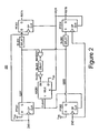
- FIG. 2 shows a block diagram of an embodiment of the frequency detector circuit of FIG. 1;
- FIG. 3 illustrates a block diagram of an embodiment of one of the counter circuits of FIG. 1, arranged in accordance with aspects of the invention.
- the meaning of “a,” “an,” and “the” includes plural reference, and the meaning of “in” includes “in” and “on.”
- the term “connected” means a direct electrical connection between the items connected, without any intermediate devices.
- the phrase “in one embodiment,” as used herein does not necessarily refer to the same embodiment, although it may.
- the term “coupled” means either a direct electrical connection between the items connected, or an indirect connection through one or more passive or active intermediary devices.
- circuit means either a single component or a multiplicity of components, either active and/or passive, that are coupled together to provide a desired function.
- signal means at least one current, voltage, charge, temperature, data, or other signal.
- the invention is related to a frequency comparator circuit that is configured to compare whether the frequency of two input signals are within a tolerance of each other.
- the frequency comparator circuit includes two counter circuits, an AND gate, and a frequency detector circuit that is configured to provide two reset signals.
- the two counter circuits are arranged to be clocked by a respective one of the two input signals, and further arranged to be reset by a respective one of the two reset signals.
- the AND gate is arranged to perform an AND function on the overflow outputs of the first and second counter circuits to provide a status signal. If the status signal is high, the difference in frequency between the two input signals is less than the tolerance. If the status signal is low, the difference in frequency between the two input signals exceeds the tolerance.
- FIG. 1 illustrates a block diagram of an embodiment of frequency comparator circuit 100 .
- Frequency comparator circuit 100 includes frequency detector circuit 120 and tolerance circuit 130 .
- An embodiment of tolerance circuit 130 includes counter circuit 110 , counter circuit 111 , and AND gate A 1 .
- frequency detector circuit 120 is configured to provide a first reset signal (RSTA) and a second reset signal (RSTB) from a first input signal (IN 1 ) and a second input signal (IN 2 ).
- RSTA first reset signal
- RSTB second reset signal
- frequency detector circuit 120 is configured to provide signals RSTA and RSTB as follows. If fIN 1 >fIN 2 , signal RSTA has a first parameter that is related to fIN 1 ⁇ fIN 2 , where fIN 1 and fIN 2 are the frequencies that are associated with signals IN 1 and IN 2 , respectively. Alternatively, if fIN 1 ⁇ fIN 2 , signal RSTB has a second parameter that is related to fIN 2 ⁇ fIN 1 .
- fRSTB is substantially zero, where fRSTB is the frequency that is associated with signal RSTB. In one embodiment, if fIN 1 ⁇ fIN 2 , fRSTA is substantially zero, where fRSTA is the frequency that is associated with signal RSTA.
- fRSTA is substantially equal to fIN 1 ⁇ fIN 2 . In one embodiment, at least if 2*fIN 1 ⁇ fIN 2 ⁇ fIN 1 , fRSTB is substantially equal to fIN 2 ⁇ fIN 1 . The difference between fIN 1 and fIN 2 is the beat frequency of signals IN 1 and IN 2 .
- Tolerance circuit 130 is configured to provide a status signal (Status) from signals IN 1 , IN 2 , RSTA, and RSTB. Further, tolerance circuit 130 is configured to provide signal Status such that signal Status corresponds to a first logic level if the difference between the fIN 1 and fIN 2 are within a tolerance window, and to a second logic level otherwise. In one embodiment, tolerance circuit 130 is arranged to provide signal Status as follows.
- Counter circuit 110 is arranged to receive signal IN 1 at a clock input of counter circuit 110
- counter circuit 111 is arranged to receive signal IN 2 at a clock input of circuit 111 . Further, counter circuit 110 is arranged to increment a first count value when a positive edge occurs in signal IN 1 . Similarly, counter circuit 111 is arranged to increment a second count value when a positive edge occurs in signal IN 1 .
- a positive edge triggered condition is described, in other embodiments, counter circuits 110 and 111 may be triggered by a negative edge, level-triggered, and the like.
- counter circuit 110 is arranged to reset the first count value (e.g. to zero) if signal RSTA is asserted.
- counter circuit 111 is arranged to reset the second count value (e.g. to zero) if signal RSTB is asserted.
- counter circuit 110 is configured to provide a first overflow signal (OF_A) at an overflow output such that signal OF_A is asserted if counter circuit 110 overflows.
- counter circuit 111 is configured to provide a second overflow signal (OF_B) at an overflow output of counter circuit 111 such that signal OF_B is asserted if counter circuit 111 overflows.
- counter circuit 110 overflows if fIN 1 ⁇ fIN 2 +tol 1
- counter circuit 111 overflows if fIN 2 ⁇ fIN 1 +tol 2
- counter circuits 110 and 111 both overflow if fIN 1 ⁇ fIN 2 ⁇ tol 1 and fIN 2 ⁇ fIN 1 ⁇ tol 2
- AND gate A 1 is arranged to provide signal Status by performing an AND function on signals OF_A and OF_B. Accordingly, signal Status has a high logic level if fIN 1 and fIN 2 are within the tolerance window of each other, and has a low logic level otherwise.
- AND gate A 1 may be replaced with another circuit that is configured to provide signal Status using the same truth table as an AND gate, and the like.
- toll is substantially given by fIN 1 /(M 1 *[fIN 1 ⁇ fIN 2 ]), where M 1 is the maximum count value of counter circuit 110 .
- tol 2 is substantially given by fIN 2 /(M 2 *[fIN 2 ⁇ fIN]), where M 2 is the maximum count value of counter circuit 111 .
- tol 1 and tol 2 provide the tolerance window, where tol 1 is an upper tolerance value for fIN 1 , and tol 2 is a lower tolerance value for fIN 1 .
- frequency comparator circuit 100 may be used for charge pump control in a phase-locked loop. In one embodiment, if signal Status is high, the charge pump provides nominal current. In this embodiment, if signal Status is low, the charge pump current is increased to speed up acquisition time.
- FIG. 2 shows a block diagram of an embodiment of frequency detector circuit 220 .
- Frequency detector circuit 220 may operate in a substantially similar manner as frequency detector circuit 120 , and may operate differently in some ways.
- Frequency detector circuit 220 includes flip-flops FF 201 -FF 204 and a clear logic circuit.
- the clear logic circuit includes delay circuits DL 201 -DL 203 , NAND gate NAND 201 , inverter INV 201 , and multiplexer MX 201 .
- the clear logic circuit may be arranged to activate a clear signal (CLR) if signal Q 301 and signal RSTA correspond to a first logic level, and arranged to deactivate signal CLEAR if at least one of signal Q 301 and signal RSTA corresponds to a second logic level.
- FF 201 may be arranged to set signal Q 301 to the first logic level in response to signal IN 1 if signal CLEAR is deactivated, and arranged to reset signal Q 301 to the second logic level if signal CLEAR is activated.
- FF 202 may be arranged to set signal RSTA to the first logic level in response to signal IN 2 if signal CLEAR is deactivated, and arranged to reset signal RSTA to the second logic level if signal CLEAR is activated.
- FF 203 may be arranged to activate signal RSTA in response to signal IN 1 if signal Q 301 corresponds to the first logic level, such that signal RSTA is activated if signal IN 1 pulses twice before signal CLEAR is activated.
- FF 204 may be arranged to activate signal RSTB in response to signal IN 2 if signal RSTA corresponds to the first logic level, such that signal RSTB is activated if signal IN 2 pulses twice before signal CLEAR is activated.
- Frequency detector circuit 220 is arranged such that signals RSTA and RSTB are dependent on fIN 1 and fIN 2 , and such that signals RSTA and RSTB are substantially independent of the phases of signals IN 1 and IN 2 .
- fRSTB is substantially zero.
- fRSTA is substantially zero.
- fRSTA is substantially given by fIN 1 ⁇ fIN 2 , and the duty cycle of signal RSTA is substantially 50%. If fIN 1 >2*fIN 2 , signal RSTA behaves in a similar manner, except that, occasionally, a pulse of signal RSTA has a pulse duration of 2/fIN 1 instead of 1/FIN 1 . If fIN 1 >>fIN 2 , fRSTA is substantially the same as fIN 2 , and the duty cycle of signal RSTA is substantially given by (fIN 1 ⁇ fIN 2 )/fIN 1 .
- fRSTB is substantially given by fIN 2 ⁇ fIN 1 , and the duty cycle of signal RSTB is substantially 50%. If fIN 2 >2*fIN 1 , RSTB behaves in a similar manner, except that, occasionally, a pulse of signal fRSTB has a pulse duration of 2/fIN 2 instead of 1/FIN 2 . If fIN 1 ⁇ fIN 2 , fRSTB is substantially the same as fIN 1 , and the duty cycle of signal RSTB is substantially given by (fIN 2 ⁇ fIN 1 )/fIN 2 .
- circuit 100 includes counter circuits 110 and 111 , further includes frequency detector circuit 220 as an embodiment of frequency detector circuit 120 , and counter circuits 110 and 111 arc both C bit counters.
- frequency detector circuit 220 as an embodiment of frequency detector circuit 120
- counter circuits 110 and 111 arc both C bit counters.
- N pulses must occur in signal IN 1 .
- the Nth pulse of signal IN 1 must happen sooner than the (N ⁇ 1)th pulse of signal IN 2 in order to propagate a logic 1 at signal RSTA (i.e. two consecutive pulses of signal IN 1 with no pulse of signal IN 2 in between).
- N*TA ⁇ (N ⁇ 1)*TB where TA and TB are the periods of signal IN 1 and signal IN 2 respectively.
- counter circuit 111 overflows. If counter circuits 110 and 111 both overflow, fIN 2 and fIN 1 are similar, within ⁇ 1/32 tolerance. If counter circuits 110 and 111 both overflow, signal Status corresponds to logic 1.
- TRSTA The time duration, TRSTA, between two single pulses of signal RSTA if fIN 1 and fIN 2 are close and fIN 1 >fIN 2 , is given by
- TRSTA 1/(fIN 1 ⁇ fIN 2 )
- FIG. 3 illustrates a block diagram of an embodiment of counter circuit 310 .
- Counter circuit 310 may operate in a substantially similar manner as counter circuit 110 , and may operate differently in some ways.
- Counter circuit 111 may be arranged in a substantially similar manner to counter circuit 310 .
- Counter circuit 310 may include flip-flops FF 1 -FF 7 , half-adders HA 1 -HA 5 , OR gates O 1 -O 2 , inverter INV 2 , multiplexer MX 2 , and delay circuit DL 4 .
- Delay circuit DL 4 is configured to provide signal IN 1 D from signal IN 1 .
- FF 1 -FF 5 are arranged as a register that is configured to store the first count value. Additionally, the register is arranged to be clocked by signal IN 1 D.
- HA 1 -HA 5 and INV 2 are arranged as a look-ahead logic circuit.
- OR gate circuit O 1 is configured to provide signal Reset from signal POR and signal RSTA.
- FF 6 and MX 2 are arranged to operate as follows.
- MX 2 is arranged to provide signal D 6 from signal Q 6 such that, when FF 6 is clocked, signal D 6 has the same logic level as signal Q 6 if signal carryA is low, and such that signal D 6 is high if signal carryA is high. Signal carryA is high only if counter 310 overflows. Additionally, Q 6 is reset to low if signal Reset is high. Accordingly, Q 6 is set high only when counter circuit 310 overflows, and only remains high until signal Reset is high.
- FF 7 is arranged to store the overflow condition.
- OR gate O 2 is arranged to provide signal OF_A such that signal OF_A is high if either Q 6 or Q 7 are high. If the overflow condition occurs, carryA changes to high, which in turn causes Q 6 to change to high, as previously described. Since Q 6 is high, OF_A is high. Next, when signal Reset changes to high, Q 6 is changed to low, and Q 7 is changed to high. At this point, OF_A remains high, since Q 7 is high. Q 7 remains high until the next leading edge of signal Reset, which causes Q 7 to change back to low.
- FF 7 and OR gate O 2 are used to temporarily store the overflow condition. If fIN 1 is greater than fIN 2 , even if signal fIN 1 is very close to fIN 2 , signal RSTA still has an occasional pulse. FF 7 and OR gate O 2 are arranged to prevent Status from immediately changing to low if this happens.
- counter circuit 310 Although one embodiment of counter circuit 310 is described above for illustrative purposes, other embodiments of counter circuit 310 are within the scope of the invention.
Landscapes
- Physics & Mathematics (AREA)
- General Physics & Mathematics (AREA)
- Manipulation Of Pulses (AREA)
Abstract
Description
Claims (20)
Priority Applications (1)
| Application Number | Priority Date | Filing Date | Title |
|---|---|---|---|
| US10/804,866 US6834093B1 (en) | 2004-03-19 | 2004-03-19 | Frequency comparator circuit |
Applications Claiming Priority (1)
| Application Number | Priority Date | Filing Date | Title |
|---|---|---|---|
| US10/804,866 US6834093B1 (en) | 2004-03-19 | 2004-03-19 | Frequency comparator circuit |
Publications (1)
| Publication Number | Publication Date |
|---|---|
| US6834093B1 true US6834093B1 (en) | 2004-12-21 |
Family
ID=33511985
Family Applications (1)
| Application Number | Title | Priority Date | Filing Date |
|---|---|---|---|
| US10/804,866 Expired - Lifetime US6834093B1 (en) | 2004-03-19 | 2004-03-19 | Frequency comparator circuit |
Country Status (1)
| Country | Link |
|---|---|
| US (1) | US6834093B1 (en) |
Cited By (21)
| Publication number | Priority date | Publication date | Assignee | Title |
|---|---|---|---|---|
| US20040113704A1 (en) * | 2002-09-13 | 2004-06-17 | Chin-Te Ho | [phase lock loop circuit and operation method thereof] |
| US20040263224A1 (en) * | 2003-04-29 | 2004-12-30 | Infineon Technologies Ag | Method for producing a control signal which indicates a frequency error |
| US20050041519A1 (en) * | 2003-07-07 | 2005-02-24 | Nazif Taskin | Integrated clock supply chip for a memory module, memory module comprising the integrated clock supply chip, and method for operating the memory module under test conditions |
| US7343510B1 (en) * | 2003-12-22 | 2008-03-11 | Cypress Semiconductor Corporation | Method and device for selecting one of multiple clock signals based on frequency differences of such clock signals |
| US20080288805A1 (en) * | 2007-05-18 | 2008-11-20 | Advanced Micro Devices, Inc. | Synchronization device and methods thereof |
| US20100295536A1 (en) * | 2009-05-22 | 2010-11-25 | Seiko Epson Corporation | Frequency measuring apparatus |
| US8593131B2 (en) | 2009-10-08 | 2013-11-26 | Seiko Epson Corporation | Signal generation circuit, frequency measurement device including the signal generation circuit, and signal generation method |
| US8643440B2 (en) | 2009-08-27 | 2014-02-04 | Seiko Epson Corporation | Electric circuit, sensor system equipped with the electric circuit, and sensor device equipped with the electric circuit |
| US8718961B2 (en) | 2009-10-06 | 2014-05-06 | Seiko Epson Corporation | Frequency measurement method, frequency measurement device and apparatus equipped with frequency measurement device |
| US9026403B2 (en) | 2010-08-31 | 2015-05-05 | Seiko Epson Corporation | Frequency measurement device and electronic device |
| RU2597954C1 (en) * | 2015-07-13 | 2016-09-20 | Федеральное государственное бюджетное образовательное учреждение высшего профессионального образования "Калининградский государственный технический университет" | Wide-range comparator of closely spaced frequencies |
| CN103986462B (en) * | 2014-05-30 | 2017-01-04 | 中国电子科技集团公司第五十八研究所 | Possesses the Fast Frequency Estimation circuit of high-speed interface |
| CN108039883A (en) * | 2017-11-21 | 2018-05-15 | 南京凌鸥创芯电子有限公司 | A kind of detection method and equipment of phaselocked loop output stable clock signal degree |
| RU2726882C1 (en) * | 2019-10-30 | 2020-07-16 | Акционерное общество "Информационные спутниковые системы"им. академика М.Ф.Решетнева" | Digital frequency comparison circuit |
| KR20200135722A (en) * | 2019-05-24 | 2020-12-03 | 윈본드 일렉트로닉스 코포레이션 | Semiconductor apparatus and continuous readout method |
| RU203487U1 (en) * | 2020-09-29 | 2021-04-07 | Закрытое Акционерное Общество "Время-Ч" | Comparator - phase analyzer |
| US20220149834A1 (en) * | 2020-11-12 | 2022-05-12 | Infineon Technologies Ag | Voltage monitoring circuit and method for monitoring a voltage |
| US20230195941A1 (en) * | 2021-12-22 | 2023-06-22 | Samsung Electronics Co., Ltd. | Malicious attack protection circuit, system-on-chip including the same, and operating method thereof |
| RU220156U1 (en) * | 2023-04-24 | 2023-08-30 | Акционерное Общество "Время-Ч" | Phase comparator-analyzer |
| TWI855584B (en) * | 2022-08-14 | 2024-09-11 | 南亞科技股份有限公司 | Clock detecting circuit |
| US20250088181A1 (en) * | 2021-12-24 | 2025-03-13 | Lx Semicon Co., Ltd. | Frequency control circuit and frequency control method |
Citations (3)
| Publication number | Priority date | Publication date | Assignee | Title |
|---|---|---|---|---|
| US5929670A (en) * | 1996-01-26 | 1999-07-27 | Hewlett-Packard Company | Method for improving signal generator frequency precision using counters |
| US6563346B2 (en) * | 2000-12-13 | 2003-05-13 | International Business Machines Corporation | Phase independent frequency comparator |
| US6642747B1 (en) | 2002-03-15 | 2003-11-04 | National Semiconductor Corporation | Frequency detector for a phase locked loop system |
-
2004
- 2004-03-19 US US10/804,866 patent/US6834093B1/en not_active Expired - Lifetime
Patent Citations (3)
| Publication number | Priority date | Publication date | Assignee | Title |
|---|---|---|---|---|
| US5929670A (en) * | 1996-01-26 | 1999-07-27 | Hewlett-Packard Company | Method for improving signal generator frequency precision using counters |
| US6563346B2 (en) * | 2000-12-13 | 2003-05-13 | International Business Machines Corporation | Phase independent frequency comparator |
| US6642747B1 (en) | 2002-03-15 | 2003-11-04 | National Semiconductor Corporation | Frequency detector for a phase locked loop system |
Cited By (30)
| Publication number | Priority date | Publication date | Assignee | Title |
|---|---|---|---|---|
| US20040113704A1 (en) * | 2002-09-13 | 2004-06-17 | Chin-Te Ho | [phase lock loop circuit and operation method thereof] |
| US20040263224A1 (en) * | 2003-04-29 | 2004-12-30 | Infineon Technologies Ag | Method for producing a control signal which indicates a frequency error |
| US7095254B2 (en) * | 2003-04-29 | 2006-08-22 | Infineon Techologies Ag | Method for producing a control signal which indicates a frequency error |
| US20050041519A1 (en) * | 2003-07-07 | 2005-02-24 | Nazif Taskin | Integrated clock supply chip for a memory module, memory module comprising the integrated clock supply chip, and method for operating the memory module under test conditions |
| US7196554B2 (en) * | 2003-07-07 | 2007-03-27 | Infineon Technologies Ag | Integrated clock supply chip for a memory module, memory module comprising the integrated clock supply chip, and method for operating the memory module under test conditions |
| US7343510B1 (en) * | 2003-12-22 | 2008-03-11 | Cypress Semiconductor Corporation | Method and device for selecting one of multiple clock signals based on frequency differences of such clock signals |
| US20080288805A1 (en) * | 2007-05-18 | 2008-11-20 | Advanced Micro Devices, Inc. | Synchronization device and methods thereof |
| US8001409B2 (en) * | 2007-05-18 | 2011-08-16 | Globalfoundries Inc. | Synchronization device and methods thereof |
| US20100295536A1 (en) * | 2009-05-22 | 2010-11-25 | Seiko Epson Corporation | Frequency measuring apparatus |
| US8664933B2 (en) * | 2009-05-22 | 2014-03-04 | Seiko Epson Corporation | Frequency measuring apparatus |
| US8643440B2 (en) | 2009-08-27 | 2014-02-04 | Seiko Epson Corporation | Electric circuit, sensor system equipped with the electric circuit, and sensor device equipped with the electric circuit |
| US8718961B2 (en) | 2009-10-06 | 2014-05-06 | Seiko Epson Corporation | Frequency measurement method, frequency measurement device and apparatus equipped with frequency measurement device |
| US8593131B2 (en) | 2009-10-08 | 2013-11-26 | Seiko Epson Corporation | Signal generation circuit, frequency measurement device including the signal generation circuit, and signal generation method |
| US9026403B2 (en) | 2010-08-31 | 2015-05-05 | Seiko Epson Corporation | Frequency measurement device and electronic device |
| CN103986462B (en) * | 2014-05-30 | 2017-01-04 | 中国电子科技集团公司第五十八研究所 | Possesses the Fast Frequency Estimation circuit of high-speed interface |
| RU2597954C1 (en) * | 2015-07-13 | 2016-09-20 | Федеральное государственное бюджетное образовательное учреждение высшего профессионального образования "Калининградский государственный технический университет" | Wide-range comparator of closely spaced frequencies |
| CN108039883A (en) * | 2017-11-21 | 2018-05-15 | 南京凌鸥创芯电子有限公司 | A kind of detection method and equipment of phaselocked loop output stable clock signal degree |
| CN108039883B (en) * | 2017-11-21 | 2021-01-29 | 南京凌鸥创芯电子有限公司 | Method and device for detecting stability of output clock signal of phase-locked loop |
| KR20200135722A (en) * | 2019-05-24 | 2020-12-03 | 윈본드 일렉트로닉스 코포레이션 | Semiconductor apparatus and continuous readout method |
| US11217315B2 (en) | 2019-05-24 | 2022-01-04 | Winbond Electronics Corp. | Semiconductor apparatus and continuous readout method |
| RU2726882C1 (en) * | 2019-10-30 | 2020-07-16 | Акционерное общество "Информационные спутниковые системы"им. академика М.Ф.Решетнева" | Digital frequency comparison circuit |
| RU203487U1 (en) * | 2020-09-29 | 2021-04-07 | Закрытое Акционерное Общество "Время-Ч" | Comparator - phase analyzer |
| US20220149834A1 (en) * | 2020-11-12 | 2022-05-12 | Infineon Technologies Ag | Voltage monitoring circuit and method for monitoring a voltage |
| US11496127B2 (en) * | 2020-11-12 | 2022-11-08 | Infineon Technologies Ag | Voltage monitoring circuit and method for monitoring a voltage |
| US20230195941A1 (en) * | 2021-12-22 | 2023-06-22 | Samsung Electronics Co., Ltd. | Malicious attack protection circuit, system-on-chip including the same, and operating method thereof |
| US12547778B2 (en) * | 2021-12-22 | 2026-02-10 | Samsung Electronics Co., Ltd. | Malicious attack protection circuit, system-on-chip including the same, and operating method thereof |
| US20250088181A1 (en) * | 2021-12-24 | 2025-03-13 | Lx Semicon Co., Ltd. | Frequency control circuit and frequency control method |
| TWI855584B (en) * | 2022-08-14 | 2024-09-11 | 南亞科技股份有限公司 | Clock detecting circuit |
| RU220156U1 (en) * | 2023-04-24 | 2023-08-30 | Акционерное Общество "Время-Ч" | Phase comparator-analyzer |
| RU221871U1 (en) * | 2023-10-05 | 2023-11-28 | Акционерное Общество "Время-Ч" | Frequency comparator |
Similar Documents
| Publication | Publication Date | Title |
|---|---|---|
| US6834093B1 (en) | Frequency comparator circuit | |
| US6642747B1 (en) | Frequency detector for a phase locked loop system | |
| US7994828B2 (en) | Frequency divider, frequency dividing method thereof, and phase locked loop utilizing the frequency divider | |
| US8471611B2 (en) | Fractional-N phase locked loop based on bang-bang detector | |
| US8401140B2 (en) | Phase/frequency detector for a phase-locked loop that samples on both rising and falling edges of a reference signal | |
| JP2002314409A (en) | Lock detection circuit | |
| JPH08237120A (en) | Method and equipment for frequency detection circuit to be used in phase synchlonous loop | |
| US8798223B2 (en) | Clock and data recovery unit without an external reference clock | |
| US6150889A (en) | Circuit and method for minimizing recovery time | |
| US6987406B1 (en) | Wide frequency range phase-locked loop circuit with phase difference | |
| US6937685B2 (en) | Apparatus and method for counting high-speed early/late pulses from a high speed phase detector using a pulse accumulator | |
| US9941890B2 (en) | Phase-locked loops with electrical overstress protection circuitry | |
| US7015727B2 (en) | Generating a lock signal indicating whether an output clock signal generated by a PLL is in lock with an input reference signal | |
| US7459964B2 (en) | Switched capacitor filter and feedback system | |
| US6275072B1 (en) | Combined phase comparator and charge pump circuit | |
| US6639958B1 (en) | Circuit configuration for the interference-free initialization of delay locked loop circuits with fast lock | |
| US7496170B2 (en) | Digitally controlled oscillator having enhanced control resolution | |
| US9374038B2 (en) | Phase frequency detector circuit | |
| US6650146B2 (en) | Digital frequency comparator | |
| US7423492B2 (en) | Circuit to reset a phase locked loop after a loss of lock | |
| JP2005252447A (en) | Lock detection circuit and method | |
| CN115021747B (en) | Delay phase-locked loop circuit, clock generation chip and electronic equipment | |
| CN107579736B (en) | hybrid lock detector | |
| US8289058B2 (en) | Multi-output PLL output shift | |
| WO2017195615A1 (en) | Detection device and detection method |
Legal Events
| Date | Code | Title | Description |
|---|---|---|---|
| AS | Assignment |
Owner name: NATIONAL SEMICONDUCTOR, CALIFORNIA Free format text: ASSIGNMENT OF ASSIGNORS INTEREST;ASSIGNOR:CHIU, HON K.;REEL/FRAME:015120/0665 Effective date: 20040318 |
|
| STCF | Information on status: patent grant |
Free format text: PATENTED CASE |
|
| AS | Assignment |
Owner name: NATIONAL SEMICONDUCTOR CORPORATION, CALIFORNIA Free format text: ASSIGNMENT OF ASSIGNORS INTEREST;ASSIGNOR:CHIU, HON KIN;REEL/FRAME:015621/0942 Effective date: 20040923 |
|
| CC | Certificate of correction | ||
| FEPP | Fee payment procedure |
Free format text: PAYOR NUMBER ASSIGNED (ORIGINAL EVENT CODE: ASPN); ENTITY STATUS OF PATENT OWNER: LARGE ENTITY |
|
| FPAY | Fee payment |
Year of fee payment: 4 |
|
| REMI | Maintenance fee reminder mailed | ||
| FPAY | Fee payment |
Year of fee payment: 8 |
|
| FPAY | Fee payment |
Year of fee payment: 12 |