US6831344B2 - Photo detect element and an optical semiconductor device - Google Patents
Photo detect element and an optical semiconductor device Download PDFInfo
- Publication number
- US6831344B2 US6831344B2 US10/401,512 US40151203A US6831344B2 US 6831344 B2 US6831344 B2 US 6831344B2 US 40151203 A US40151203 A US 40151203A US 6831344 B2 US6831344 B2 US 6831344B2
- Authority
- US
- United States
- Prior art keywords
- photodiode
- optical semiconductor
- semiconductor device
- detect element
- photo
- Prior art date
- Legal status (The legal status is an assumption and is not a legal conclusion. Google has not performed a legal analysis and makes no representation as to the accuracy of the status listed.)
- Expired - Lifetime, expires
Links
Images


Classifications
-
- H—ELECTRICITY
- H10—SEMICONDUCTOR DEVICES; ELECTRIC SOLID-STATE DEVICES NOT OTHERWISE PROVIDED FOR
- H10D—INORGANIC ELECTRIC SEMICONDUCTOR DEVICES
- H10D62/00—Semiconductor bodies, or regions thereof, of devices having potential barriers
- H10D62/10—Shapes, relative sizes or dispositions of the regions of the semiconductor bodies; Shapes of the semiconductor bodies
- H10D62/102—Constructional design considerations for preventing surface leakage or controlling electric field concentration
- H10D62/103—Constructional design considerations for preventing surface leakage or controlling electric field concentration for increasing or controlling the breakdown voltage of reverse-biased devices
- H10D62/105—Constructional design considerations for preventing surface leakage or controlling electric field concentration for increasing or controlling the breakdown voltage of reverse-biased devices by having particular doping profiles, shapes or arrangements of PN junctions; by having supplementary regions, e.g. junction termination extension [JTE]
- H10D62/109—Reduced surface field [RESURF] PN junction structures
- H10D62/111—Multiple RESURF structures, e.g. double RESURF or 3D-RESURF structures
-
- H—ELECTRICITY
- H10—SEMICONDUCTOR DEVICES; ELECTRIC SOLID-STATE DEVICES NOT OTHERWISE PROVIDED FOR
- H10F—INORGANIC SEMICONDUCTOR DEVICES SENSITIVE TO INFRARED RADIATION, LIGHT, ELECTROMAGNETIC RADIATION OF SHORTER WAVELENGTH OR CORPUSCULAR RADIATION
- H10F77/00—Constructional details of devices covered by this subclass
- H10F77/40—Optical elements or arrangements
- H10F77/413—Optical elements or arrangements directly associated or integrated with the devices, e.g. back reflectors
-
- H—ELECTRICITY
- H10—SEMICONDUCTOR DEVICES; ELECTRIC SOLID-STATE DEVICES NOT OTHERWISE PROVIDED FOR
- H10F—INORGANIC SEMICONDUCTOR DEVICES SENSITIVE TO INFRARED RADIATION, LIGHT, ELECTROMAGNETIC RADIATION OF SHORTER WAVELENGTH OR CORPUSCULAR RADIATION
- H10F30/00—Individual radiation-sensitive semiconductor devices in which radiation controls the flow of current through the devices, e.g. photodetectors
- H10F30/20—Individual radiation-sensitive semiconductor devices in which radiation controls the flow of current through the devices, e.g. photodetectors the devices having potential barriers, e.g. phototransistors
- H10F30/21—Individual radiation-sensitive semiconductor devices in which radiation controls the flow of current through the devices, e.g. photodetectors the devices having potential barriers, e.g. phototransistors the devices being sensitive to infrared, visible or ultraviolet radiation
- H10F30/288—Individual radiation-sensitive semiconductor devices in which radiation controls the flow of current through the devices, e.g. photodetectors the devices having potential barriers, e.g. phototransistors the devices being sensitive to infrared, visible or ultraviolet radiation the devices being sensitive to multiple wavelengths, e.g. multi-spectrum radiation detection devices
-
- H—ELECTRICITY
- H10—SEMICONDUCTOR DEVICES; ELECTRIC SOLID-STATE DEVICES NOT OTHERWISE PROVIDED FOR
- H10F—INORGANIC SEMICONDUCTOR DEVICES SENSITIVE TO INFRARED RADIATION, LIGHT, ELECTROMAGNETIC RADIATION OF SHORTER WAVELENGTH OR CORPUSCULAR RADIATION
- H10F77/00—Constructional details of devices covered by this subclass
- H10F77/50—Encapsulations or containers
-
- H—ELECTRICITY
- H10—SEMICONDUCTOR DEVICES; ELECTRIC SOLID-STATE DEVICES NOT OTHERWISE PROVIDED FOR
- H10W—GENERIC PACKAGES, INTERCONNECTIONS, CONNECTORS OR OTHER CONSTRUCTIONAL DETAILS OF DEVICES COVERED BY CLASS H10
- H10W90/00—Package configurations
- H10W90/701—Package configurations characterised by the relative positions of pads or connectors relative to package parts
- H10W90/751—Package configurations characterised by the relative positions of pads or connectors relative to package parts of bond wires
- H10W90/756—Package configurations characterised by the relative positions of pads or connectors relative to package parts of bond wires between a chip and a stacked lead frame, conducting package substrate or heat sink
Definitions
- the present invention relates to a photo detect element and an optical semiconductor device and, more particularly, to an optical semiconductor device that is used in so-called visual sensitivity and luminous intensity measurement etc. for measuring luminous intensity by sensing visible light only.
- a single chipped photo detect element comprising photo diodes (hereafter, referred to as PD) and an amplifying operation processing circuit to perform the amplification and processing of optical signals from PD are used.
- PD photo diodes
- an amplifying operation processing circuit to perform the amplification and processing of optical signals from PD.
- an n-type region 2 is formed on the surface of a p-type silicon substrate 1 and a p-type region 3 is formed on the surface of this n-type region 2 .
- two PD (PD 1 4 , PD 2 5 ) are formed.
- An optical absorption rate on Si wafer varies depending on a depth from the surface and this optical absorption depth dependency differs depending on a wavelength, as shown FIG. 9 .
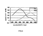
- the spectral response characteristic differs for each PD, for example, as shown in FIG. 3 .
- the photodiode PD 1 has the maximum sensitivity at around a wavelength 600 nm and the photodiode PD 2 at the position deeper than the photodiode PD 1 has the maximum sensitivity at around a wavelength 900 nm in FIG. 3 .
- a predetermined sensibility that is, visual sensitivity
- a photo detect element by processing outputs from the diodes PD 1 and PD 2 that have different spectral response characteristics through the amplifying operation processing circuit.
- the luminous intensity corresponding to the spectral luminous efficiency is measured by eliminating the infrared component of the output of the photodiode PD 1 using the infrared component of the output of the PD 2 .
- a photo detect element 10 having such characteristic as this is mounted on a glass epoxy resin (hereinafter referred to as Glass-Epoxy) made substrate and the like, cured and bonded thereon, as shown in FIGS. 10A-10D, and FIG. 11 .
- a glass epoxy resin hereinafter referred to as Glass-Epoxy
- an enclosure is formed and separated after transfer molded by a transparent epoxy resin 14 in order to protect the photo detect element 10 .
- the photo detect element 10 is connected to an external circuit in a metallized portion 16 .
- the optical semiconductor device carriers are generated by infrared ray incoming from the side of the photo semiconductor unit and a dicing face of the photo detect element, infrared ray near 1000 nm turned around in the photo detect element.
- the photo detect element gets a sub-peak of unnecessary infrared component of 900-1200 nm (centering around 1000 nm) in addition to a peak of visual sensitivity (550 nm) as shown in FIG. 8 . That is, as a conventional optical semiconductor device detects unnecessary infrared component, the illumination intensity corresponding to spectral luminance efficiency could not be made.
- an optical semiconductor device used for detecting spectral luminance efficiency a defect is produced as a peak is detected in the infrared region.
- a light source ratio A light source/fluorescent lamp
- an optical semiconductor device having a characteristic to sense a sub-peak of a visual sensitivity in the above-mentioned infrared region senses the infrared region and when components of the infrared region of A light source are sensed, an output current value increases and a light source ratio becomes worse.
- flat and reflective materials for example, white glass epoxy resin plate, etc.
- the infrared component region is also reflected by the reflection of light from the substrate and the light source ratio is made further worse.
- a conventional optical semiconductor device has a sensing character in the infrared region and therefore, there was such a problem that the output also depends on infrared ray when a optical semiconductor device is used for visual sensing of luminous intensity.
- an object of the present invention is to provide an optical semiconductor device with its spectral sensitivity characteristic controlled more precisely by suppressing the sensitivity in an infrared region with such a defect of a conventional optical semiconductor device removed.
- the optical semiconductor device of the present invention is characterized in that an n-type region is formed on a p-type substrate, a p-type region is formed on the surface of this n-type region, a photo detect element equipped with a first photo diode having peak wavelength sensitivity in a visible spectral region is provided on the interface between the n-type region and the p-type region, a second photo diode having peak wavelength sensitivity in the infrared region is provided on the interface between the p-type substrate and the n-type region, and specific resistance R of the p-type substrate is 1 ⁇ R ⁇ 3( ⁇ cm).
- FIG. 1 is a cross-sectional view showing PD 1 , PD 2 used in en embodiment of the present invention
- FIG. 2 is a circuit diagram of an photo detect element used in an embodiment of the present invention.
- FIG. 3 is a diagram showing the spectral sensitivity characteristics of PD 1 , and PD 2 used in an embodiment of the present invention
- FIG. 4 is a top view of an example of a photo detect element used in an embodiment of the present invention viewed from the above;
- FIG. 5 A ⁇ FIG. 5D are diagrams showing the construction of a opt semiconductor device in an embodiment of an present invention.
- FIG. 6 A and FIG. 6B are a plan view and a cross-sectional view of an optical semiconductor device in an embodiment of the present invention.
- FIG. 7 A and FIG. 7B are diagrams showing the spectral sensitivity characteristic of an optical semiconductor device in an embodiment of the present invention.
- FIG. 8 is a diagram showing the spectral sensitivity characteristic of a conventional optical semiconductor device
- FIG. 9 is a diagram showing the depth dependency of optical absorption in Si wafer.
- FIG. 10 A ⁇ FIG. 10B are diagrams showing a conventional optical semiconductor device
- FIG. 11 is a diagram showing a conventional optical semiconductor device.
- FIG. 12 is a diagram showing a spectral sensitivity characteristic of the photodiodes PD 1 , PD 2 when a filter provided in the photo acceptance portion is in the thin film laminated structure in an embodiment of the present invention.
- FIG. 1 through FIG. 8 An embodiment of the present invention will be described below in detail referring to FIG. 1 through FIG. 8 .
- an n-type region 2 and a p-type region 3 are formed on the surface of a p-type silicon substrate 1 and a photo acceptance portion having PD 1 4 and PD 2 5 is formed. Further, a filter 6 is formed on the surface An amplifying and an arithmetic circuit is formed with this photo acceptance portion.
- the PD 1 and PD 2 of the photo detect element convert photo signals into electric signals PD 1 , PD 2 , which are then output through an initial stage amplifier, a differential circuit, an arithmetic circuit and an amplifier. Further, the spectral sensitivity characteristic of PD 1 and PD 2 is the same as before as shown in FIG. 3 .
- a photo detect element 10 is formed by arranging a photo detect part 7 , an amplifying operation processing circuit 8 , a bonding pad 9 and diced as shown in FIG. 4 . Then, the photo detect element 10 is mounted on a mount bed 12 and terminals of the photo detect element 10 are bonded to a metallic lead frame 11 with a gold wire 13 shown in an external view in FIG. 8 A and FIG. 8B, a plan view and a cross-sectional view in FIG. 6 A and FIG. 6 B. Thereafter, an enclosure is molded and formed by an transparent epoxy resin 14 to protect the photo detect element 10 and an optical semiconductor device is formed and connected to an external circuit at the outer lead portion of the exposed metallic lead frame 11 .
- Iout mXIp 1 ⁇ nX ( Ip 1 +Ip 2 ).
- Iout ⁇ ( Ip 1 ⁇ Ip 2 ).
- coefficient of amplification ⁇ is a value set by a demanded output current value.
- a photo detect space S of the photo detect part is 0.1225 mm 2 (0.35 mm square).
- this coefficient of subtraction magnification ⁇ is especially effective when the photo detecting space C is below 0.25 and is
- a p-type substrate having a high resistivity of 4 ⁇ 6 ⁇ cm was so far used for substrate of photo detect element.
- substrate resistivity R the more low the substrate resistivity R is, the more preferable in order to reduce light source ratio and infrared component.
- substrate resistivity R is less than 1 ⁇ cm, it does not function as PD.
- a sufficient effect cannot be obtained and 1 ⁇ 3 ⁇ cm is adequate.
- a desired value of substrate resistivity can be obtained by adjusting the doping amount of p-type impurity.
- a light source ratio and relative strength of infrared component when a chip thickness dc of a photo detect element shown in FIG. 5D were obtained as shown in Table 2. Further, a package thickness dp of an optical semiconductor device is 0.7 mm and a metallic lead frame in 0.1 ⁇ 0.15 mm thick is used.
- Chip thickness dp of the photo detect element was made to 0.3 mm by lapping.
- Chip thickness dc/package thickness dp (chip thickness ratio) was 40 ⁇ 55% for the package thickness dp about 0.55 ⁇ 0.7 mm of an optical semiconductor device.
- slight source ratio and infrared component can be reduced by reducing the chip thickness dc to 0.2 mm or below (0.05 mm or more is realistic).
- the chip thickness ratio (dc/dp) below 0.25 is good (0.07 or more is realistic) and 0.2 or below is preferable.
- the mount bed is a portion of the lead frame on which a photo detect element is mounted.
- FIG. 6 A and FIG. 6B that is equivalent to the cross sectional diagram of Section A—A in FIG. 6A, what is equivalent to the length of one side is substantially a mount bed size tm.
- ⁇ t is given by the following formula:
- ⁇ t is equivalent to a distance between the edge of the mount bed 12 when the photo detect element 10 is mounted at the center of the mount bed 12 and the edge of the photo detect element 10 . Further, when ⁇ t differs depending on a position, its maximum value is made as ⁇ t.
- the chip size tc is 1.1 mm.
- light source ratio and infrared component can be suppressed by reducing ⁇ t to below 0.1 mm. This is because the reflection of light including infrared component from the mount bed is suppressed, and it is ideal to make the chip size tc equal to the mount bed size tm. Further, it is preferred not to mount anything reflecting light in a range within 0.1 mm around the mount bed 12 .
- the mount bed 12 is made here as the photo detect element mounting part of the metallic lead frame 11 . This is also the same on ball Grid Array (BGA) substrate, etc. and it is effective to suppress the distance from the photo detect element to the mount bed edge similarly. At this time, it is necessary to make regions other than the mount bed 12 of the substrate using material and color (black) not reflecting light.
- BGA ball Grid Array
- FIG. 7A is a spectral sensitivity characteristic diagram showing relative sensitivity of Package B with a low substrate resistivity R (2 ⁇ 3 ⁇ cm) and an optimized coefficient of subtraction magnification ⁇ to wavelengths.
- FIG. 7B is a spectral sensitivity characteristic diagram showing relative sensitivity of an improved Package A with optimized chip thickness ratio and ⁇ t.
- a good spectral sensitivity characteristic with almost less sensitivity in the infrared region is obtained in FIG. 7 B.
- FIG. 7A a good spectral sensitivity characteristic was obtained though certain sensitivity was left in the infrared region and it is seen that the optimization of parameters is also effective in Package B.
- a printing substrate needs to make it the quality of the material which does not reflect light, and a color (black).
- the filter 6 having the characteristic to shut off infrared components when used, the sensitivity in the infrared region can be further reduced and an optical semiconductor device having more high precisely controlled spectral sensitivity characteristic can be obtained.
- the filter 6 is formed by laminating, for example, a thin film of titanium dioxide (TiO 2 ) having a high refractive index and a thin film of silicon dioxide (SiO 2 ) alternately.
- the thin film titanium dioxide and thin film silicon dioxide are, for example, 0.24 ⁇ m thick and laminated by, for example, deposition for every 75 layers to a filter of total 150 layers and total thickness 36 ⁇ m.
- Deposition conditions when laminating titanium dioxide and silicon dioxide by deposing are, for example, degree of vacuum is 1 Pa ⁇ 2 ⁇ 10 ⁇ 4 Pa, substrate temperature 120 ⁇ 350° C., and resistance heating or an electron gun is used.
- the total number of films that are laminated for the filter 6 is selected in a range of about 50 ⁇ 150 layers.
- a filter in this laminated structure is formed by deposition directly on the photo detect part.
- Spectral sensitivity characteristic by photodiodes PD 1 and PD 2 when the photo detect part has a filter in the laminated structure formed as described above is shown in FIG. 12 .
- the characteristic of the photodiode PD 1 is B 1
- the characteristic of the photodiode PD 2 is B 2 .
- B 1 , B 2 are compared with the characteristic shown in FIG. 3, it is seen that when a filter in the laminated structure is used, the wavelength is around 650 nm or above and spectral sensitivity was lowered and spectral sensitivity at a wavelength above 800 nm is nearly zero and almost constant.
- an optical semiconductor device having the suppressed sensitivity in the infrared region and a high precisely controlled spectral sensitivity character.
Landscapes
- Light Receiving Elements (AREA)
Abstract
An optical semiconductor device of the present invention is equipped with a photo detect element 10 comprising a photo detect part 7 provided with two photodiodes having two photodiodes having peak wavelength sensitivity in a visible light region and an infrared region, respectively and an amplifying operation processing circuit 8 for amplifying and processing outputs of the photodiodes, and characterized in that substrate resistivity R is as follows:
Description
This application is based upon and claims the benefit of priority from the prior Japanese Patent Applications No. 2002-97046, filed on Mar. 29, 2002: the entire contents of which are incorporated herein by reference.
1. Field of the Invention
The present invention relates to a photo detect element and an optical semiconductor device and, more particularly, to an optical semiconductor device that is used in so-called visual sensitivity and luminous intensity measurement etc. for measuring luminous intensity by sensing visible light only.
2. Description of Related Art
In recent years, in optical semiconductor devices that are used for visual sensitivity and luminous intensity measurement, a single chipped photo detect element comprising photo diodes (hereafter, referred to as PD) and an amplifying operation processing circuit to perform the amplification and processing of optical signals from PD are used. As shown in FIG. 1, an n-type region 2 is formed on the surface of a p-type silicon substrate 1 and a p-type region 3 is formed on the surface of this n-type region 2. At two PN junctions formed in the vertical direction, two PD (PD 1 4, PD2 5) are formed.
An optical absorption rate on Si wafer varies depending on a depth from the surface and this optical absorption depth dependency differs depending on a wavelength, as shown FIG. 9. As the distances of above-mentioned two PN junctions from the surface of the substrate are different, the spectral response characteristic differs for each PD, for example, as shown in FIG. 3. The photodiode PD1 has the maximum sensitivity at around a wavelength 600 nm and the photodiode PD2 at the position deeper than the photodiode PD1 has the maximum sensitivity at around a wavelength 900 nm in FIG. 3.
Thus, a predetermined sensibility; that is, visual sensitivity can be obtained by a photo detect element by processing outputs from the diodes PD1 and PD2 that have different spectral response characteristics through the amplifying operation processing circuit. The luminous intensity corresponding to the spectral luminous efficiency is measured by eliminating the infrared component of the output of the photodiode PD1 using the infrared component of the output of the PD2.
A photo detect element 10 having such characteristic as this is mounted on a glass epoxy resin (hereinafter referred to as Glass-Epoxy) made substrate and the like, cured and bonded thereon, as shown in FIGS. 10A-10D, and FIG. 11. After bonding the terminals of the photo detect element with gold wires, an enclosure is formed and separated after transfer molded by a transparent epoxy resin 14 in order to protect the photo detect element 10. Then, the photo detect element 10 is connected to an external circuit in a metallized portion 16.
In such the optical semiconductor device, carriers are generated by infrared ray incoming from the side of the photo semiconductor unit and a dicing face of the photo detect element, infrared ray near 1000 nm turned around in the photo detect element. As a result, the photo detect element gets a sub-peak of unnecessary infrared component of 900-1200 nm (centering around 1000 nm) in addition to a peak of visual sensitivity (550 nm) as shown in FIG. 8. That is, as a conventional optical semiconductor device detects unnecessary infrared component, the illumination intensity corresponding to spectral luminance efficiency could not be made.
That is, as an optical semiconductor device used for detecting spectral luminance efficiency, a defect is produced as a peak is detected in the infrared region. For example, when two light sources are set at the same luminous intensity, there is originally no difference in optical output current values and a light source ratio (A light source/fluorescent lamp) is one time. However, an optical semiconductor device having a characteristic to sense a sub-peak of a visual sensitivity in the above-mentioned infrared region senses the infrared region and when components of the infrared region of A light source are sensed, an output current value increases and a light source ratio becomes worse. Further, when flat and reflective materials (for example, white glass epoxy resin plate, etc.) are used for a substrate to install a photo detect element, the infrared component region is also reflected by the reflection of light from the substrate and the light source ratio is made further worse.
As explained in the above, a conventional optical semiconductor device has a sensing character in the infrared region and therefore, there was such a problem that the output also depends on infrared ray when a optical semiconductor device is used for visual sensing of luminous intensity.
Therefore, an object of the present invention is to provide an optical semiconductor device with its spectral sensitivity characteristic controlled more precisely by suppressing the sensitivity in an infrared region with such a defect of a conventional optical semiconductor device removed.
The optical semiconductor device of the present invention is characterized in that an n-type region is formed on a p-type substrate, a p-type region is formed on the surface of this n-type region, a photo detect element equipped with a first photo diode having peak wavelength sensitivity in a visible spectral region is provided on the interface between the n-type region and the p-type region, a second photo diode having peak wavelength sensitivity in the infrared region is provided on the interface between the p-type substrate and the n-type region, and specific resistance R of the p-type substrate is 1≦R≦3(Ωcm).
FIG. 1 is a cross-sectional view showing PD1, PD2 used in en embodiment of the present invention;
FIG. 2 is a circuit diagram of an photo detect element used in an embodiment of the present invention;
FIG. 3 is a diagram showing the spectral sensitivity characteristics of PD1, and PD2 used in an embodiment of the present invention;
FIG. 4 is a top view of an example of a photo detect element used in an embodiment of the present invention viewed from the above;
FIG. 5A˜FIG. 5D are diagrams showing the construction of a opt semiconductor device in an embodiment of an present invention;
FIG. 6A and FIG. 6B are a plan view and a cross-sectional view of an optical semiconductor device in an embodiment of the present invention.
FIG. 7A and FIG. 7B are diagrams showing the spectral sensitivity characteristic of an optical semiconductor device in an embodiment of the present invention;
FIG. 8 is a diagram showing the spectral sensitivity characteristic of a conventional optical semiconductor device;
FIG. 9 is a diagram showing the depth dependency of optical absorption in Si wafer;
FIG. 10A˜FIG. 10B are diagrams showing a conventional optical semiconductor device;
FIG. 11 is a diagram showing a conventional optical semiconductor device; and
FIG. 12 is a diagram showing a spectral sensitivity characteristic of the photodiodes PD1, PD2 when a filter provided in the photo acceptance portion is in the thin film laminated structure in an embodiment of the present invention.
An embodiment of the present invention will be described below in detail referring to FIG. 1 through FIG. 8.
As shown in FIG. 1, an n-type region 2 and a p-type region 3 are formed on the surface of a p-type silicon substrate 1 and a photo acceptance portion having PD 1 4 and PD 2 5 is formed. Further, a filter 6 is formed on the surface An amplifying and an arithmetic circuit is formed with this photo acceptance portion. As shown in FIG. 2, in this operational amplifier, the PD1 and PD2 of the photo detect element convert photo signals into electric signals PD1, PD2, which are then output through an initial stage amplifier, a differential circuit, an arithmetic circuit and an amplifier. Further, the spectral sensitivity characteristic of PD1 and PD2 is the same as before as shown in FIG. 3.
Then, a photo detect element 10 is formed by arranging a photo detect part 7, an amplifying operation processing circuit 8, a bonding pad 9 and diced as shown in FIG. 4. Then, the photo detect element 10 is mounted on a mount bed 12 and terminals of the photo detect element 10 are bonded to a metallic lead frame 11 with a gold wire 13 shown in an external view in FIG. 8A and FIG. 8B, a plan view and a cross-sectional view in FIG. 6A and FIG. 6B. Thereafter, an enclosure is molded and formed by an transparent epoxy resin 14 to protect the photo detect element 10 and an optical semiconductor device is formed and connected to an external circuit at the outer lead portion of the exposed metallic lead frame 11.
In such the optical semiconductor device, when the output current by PD1, PD2 are IP1, IP2 and processed through the amplifying operation processing circuit, the entire output current Iout becomes as shown below:
That is,
α: Coefficient of subtraction factor (n/(m−n))
β: Coefficient of amplification (m−n) Further, coefficient of amplification β is a value set by a demanded output current value. A photo detect space S of the photo detect part is 0.1225 mm2 (0.35 mm square).
With regard to Package A of an optical semiconductor device that is formed as described above and Package B that is formed with a similar photo detect element mounted on a glass epoxy substrate and transfer molded, a luminous source ratio when a coefficient of subtraction factor and a resistivity of a p-type silicon substrate were changed and peak relative strength of infrared component to peak strength are obtained as shown in Table 1.
| TABLE 1 | |||||
| luminous | |||||
| Resistivity | source | infrared | |||
| # | Package | (Ω cm) | α | ratio | component |
| 1 | A | 2˜3 | 0.3 | 1˜1.5 | 5% |
| 2 | 0.55 | 0.9˜1.2 | 5% | ||
| 3 | 1 | 2˜4 | 10% | ||
| 4 | 4˜6 | 0.3 | 1.5˜2 | 20% | |
| 5 | |
2˜3 | 0.3 | 1.5˜2 | 30% |
| 6 | 1 | 2˜4 | 30% | ||
| 7 | 4˜6 | 0.3 | 2˜3 | 50% | |
| 8 | 1 | 3˜6 | 50% | ||
So far, a coefficient of subtraction magnification α was not taken into consideration. That is, α=1 and it was seen that it becomes possible to reduce a luminous source ratio and infrared component when the coefficient of subtraction magnification a is set in the following range.
Further, the range of this coefficient of subtraction magnification αis especially effective when the photo detecting space C is below 0.25 and is
Further, in an effort to improve reliability of an optical semiconductor device and extend its life, a p-type substrate having a high resistivity of 4˜6 Ωcm was so far used for substrate of photo detect element. However, it is seen that it becomes possible to reduce a light source ratio and infrared component by controlling the number of lattice defects of p-type substrate and using substrate having a low resistivity of 2˜3 Ωcm inversely in this embodiment. This is considered because when substrate resistivity R becomes low, spectral sensitivity characteristic shifts to higher energy of photon than absorption band gap, that is, to the short wavelength side at lower substrate resistivity R.
Further, the more low the substrate resistivity R is, the more preferable in order to reduce light source ratio and infrared component. However, when substrate resistivity R is less than 1 Ωcm, it does not function as PD. On the other hand, over 3 Ωcm, a sufficient effect cannot be obtained and 1˜3 Ωcm is adequate. Further, a desired value of substrate resistivity can be obtained by adjusting the doping amount of p-type impurity.
Further, with regard to an optical semiconductor device similarly formed, a light source ratio and relative strength of infrared component when a chip thickness dc of a photo detect element shown in FIG. 5D were obtained as shown in Table 2. Further, a package thickness dp of an optical semiconductor device is 0.7 mm and a metallic lead frame in 0.1˜0.15 mm thick is used.
| TABLE 2 | ||||||
| chip | luminous | |||||
| Resistivity | thickness | source | infrared | |||
| # | package | (Ω cm) | α | dp (mm) | ratio | component |
| 9 | A | 2˜3 | 0.55 | 0.1 | 0.85˜1.1 | 3% |
| 10 | 0.15 | 0.9˜1.2 | 5% | |||
| 11 | 0.2 | 1˜1.5 | 8% | |||
| 12 | 0.3 | 1˜1.5 | 10% | |||
| 13 | B | 0.3 | 0.3 | 1.5˜2 | 30% | |
So far, the chip thickness dp of the photo detect element was made to 0.3 mm by lapping. Chip thickness dc/package thickness dp (chip thickness ratio) was 40˜55% for the package thickness dp about 0.55˜0.7 mm of an optical semiconductor device. However, it is seen that slight source ratio and infrared component can be reduced by reducing the chip thickness dc to 0.2 mm or below (0.05 mm or more is realistic). The chip thickness ratio (dc/dp) below 0.25 is good (0.07 or more is realistic) and 0.2 or below is preferable.
When the chip thickness ratio (dc/dp) is made to 0.25 or below, generation of crack by coefficient of expansion of the transparent epoxy resin 14, the photo detect element 10 and the metallic lead frame 11 can be prevented.
Further, with regard to an optical semiconductor device (Package A) that is similarly formed, light source ratio and relative strength of infrared component when a mount bed size of a metallic lead frame on which the photo detect element is installed were changed are obtained with the results as shown in Table 3.
Here, the mount bed is a portion of the lead frame on which a photo detect element is mounted. As shown in FIG. 6A and FIG. 6B that is equivalent to the cross sectional diagram of Section A—A in FIG. 6A, what is equivalent to the length of one side is substantially a mount bed size tm. Further, when a chip size is tc, Δt is given by the following formula:
Δt is equivalent to a distance between the edge of the mount bed 12 when the photo detect element 10 is mounted at the center of the mount bed 12 and the edge of the photo detect element 10. Further, when Δt differs depending on a position, its maximum value is made as Δt. The chip size tc is 1.1 mm.
| TABLE 3 | |||||
| luminous | infrared | ||||
| # | tm (mm) | Δt (mm) | | component | |
| 14 | 1.1 | 0 | 0.9˜1.3 | 3% |
| 15 | 1.2 | 0.05 | 0.9˜1.3 | 5% |
| 16 | 1.3 | 0.1 | 1˜1.5 | 8% |
| 17 | 1.4 | 0.15 | 2˜3 | 10% |
| 18 | 1.5 | 0.2 | 2˜3 | 12% |
Thus, it can be seen that light source ratio and infrared component can be suppressed by reducing Δt to below 0.1 mm. This is because the reflection of light including infrared component from the mount bed is suppressed, and it is ideal to make the chip size tc equal to the mount bed size tm. Further, it is preferred not to mount anything reflecting light in a range within 0.1 mm around the mount bed 12.
Further, the mount bed 12 is made here as the photo detect element mounting part of the metallic lead frame 11. This is also the same on ball Grid Array (BGA) substrate, etc. and it is effective to suppress the distance from the photo detect element to the mount bed edge similarly. At this time, it is necessary to make regions other than the mount bed 12 of the substrate using material and color (black) not reflecting light.
Further, in this embodiment, a case wherein the chip size tc is below 1.1 mm is described. However, even when it is below 1.1 mm, if Δt is below 0.1 mm, it is possible to reduce infrared component sufficiently. However, when Δt=0.1 mm or below, it is needless to say that infrared component can be reduced relatively in a large chip size.
Further, the spectral responsibility was measured on optical semiconductor devices formed as described above with the results shown in FIG. 7A and FIG. 7B. Further, FIG. 7A is a spectral sensitivity characteristic diagram showing relative sensitivity of Package B with a low substrate resistivity R (2˜3 Ωcm) and an optimized coefficient of subtraction magnification α to wavelengths. FIG. 7B is a spectral sensitivity characteristic diagram showing relative sensitivity of an improved Package A with optimized chip thickness ratio and Δt.
It is seen that the spectral sensitivity characteristic shown in FIG. 7A and FIG. 7B is sharply improved when compared with the spectral sensitivity characteristic of a conventional optical semiconductor device (Package B of α=1, high substrate resistivity). In particular, a good spectral sensitivity characteristic with almost less sensitivity in the infrared region is obtained in FIG. 7B. Also in FIG. 7A, a good spectral sensitivity characteristic was obtained though certain sensitivity was left in the infrared region and it is seen that the optimization of parameters is also effective in Package B.
In addition, in Package B, a printing substrate needs to make it the quality of the material which does not reflect light, and a color (black).
Further, in the construction diagram of the photo detect part shown in FIG. 1, when the filter 6 having the characteristic to shut off infrared components is used, the sensitivity in the infrared region can be further reduced and an optical semiconductor device having more high precisely controlled spectral sensitivity characteristic can be obtained.
The filter 6 is formed by laminating, for example, a thin film of titanium dioxide (TiO2) having a high refractive index and a thin film of silicon dioxide (SiO2) alternately. The thin film titanium dioxide and thin film silicon dioxide are, for example, 0.24 μm thick and laminated by, for example, deposition for every 75 layers to a filter of total 150 layers and total thickness 36 μm.
Deposition conditions when laminating titanium dioxide and silicon dioxide by deposing are, for example, degree of vacuum is 1 Pa˜2×10⁻⁴ Pa, substrate temperature 120˜350° C., and resistance heating or an electron gun is used.
Further, the total number of films that are laminated for the filter 6 is selected in a range of about 50˜150 layers. A filter in this laminated structure is formed by deposition directly on the photo detect part.
Spectral sensitivity characteristic by photodiodes PD1 and PD2 when the photo detect part has a filter in the laminated structure formed as described above is shown in FIG. 12. The characteristic of the photodiode PD1 is B1 and the characteristic of the photodiode PD2 is B2. When these characteristics B1, B2 are compared with the characteristic shown in FIG. 3, it is seen that when a filter in the laminated structure is used, the wavelength is around 650 nm or above and spectral sensitivity was lowered and spectral sensitivity at a wavelength above 800 nm is nearly zero and almost constant.
As described above, when a filter with thin films having different refraction factors laminated alternately is directly provided to the photo detect part, a further good spectral sensitivity characteristic can be obtained irrespective of incident range of light.
When this filter in laminated structure is provided to the photo detect part by the deposition, there is the less possibility of separation by heat generated when soldered or secular change of the fixed portion even when the filter is mounted on the surface of a wiring substrate, etc. by the reflow soldering and a highly reliable optical semiconductor device is obtained.
According to the present invention, it is possible to provide an optical semiconductor device having the suppressed sensitivity in the infrared region and a high precisely controlled spectral sensitivity character.
Claims (12)
1. A photo detect element comprising:
a first photodiode having peak wavelength sensitivity in a visible light region;
a second photodiode having peak wavelength sensitivity in an infrared region;
wherein said first photodiode comprises a p-type substrate and a n-type region on said p-type substrate, and
said second photodiode comprises said n-type region and said p-type region on said n-type region, and
resistivity R of said p-type substrate is as follow:
2. A photo detect element according to claim 1 , wherein when a thickness of said optical semiconductor device is assumed to be dc,
is satisfied.
3. An optical semiconductor device comprising:
a photo detect element equipped with a first photodiode having peak wave length sensitivity in a visible light region and a second photodiode having peak wavelength sensitivity in an infrared region;
a package covering said photo detect element;
wherein when a thickness ratio of the optical semiconductor dc/a thickness of the package dp
is satisfied.
4. An optical semiconductor device comprising:
a photo detect element equipped with a first photodiode having peak wave length sensitivity in a visible light region and a second photodiode having peak wavelength sensitivity in an infrared region;
a mount bed with a transparent resin portion covering the photo detect element and the photo detect element mounted thereon; and
a means for connecting to an external circuit,
and when the mount bed size is tm and the size of the photo detect element is tc and when
is satisfied.
5. An optical semiconductor device comprising:
a photo detect element equipped with a first photodiode having peak wavelength sensitivity in a visible light region and a second photodiode having peak wavelength sensitivity in an infrared region; and
an amplifying operation processing circuit for processing and outputting an output current IP1 from said first photodiode and an output current IP2 from said second photo diode; and
wherein when α is assumed to be a coefficient of subtraction magnification and β is assumed to be a coefficient of amplification, an output Iout from said amplifying operation processing circuit obtained by the following formula,
6. An optical semiconductor device according to claim 3 or 4 ,
wherein a space S of a photo detecting part is as follows:
7. An optical semiconductor device comprising:
a photo detect element equipped with a first photodiode having peak wave length sensitivity in a visible light region and a second photodiode having peak wavelength sensitivity in an infrared region;
a package covering said photo detect element; and
a filter formed on said photo detect element by laminating plural kinds of films having different refraction factors by deposition,
wherein said first photodiode comprises a p-type substrate and a n-type region on said p-type substrate, and said second photodiode comprises said n-type region and said p-type region on said n-type region, and
a resistivity R of said p-type substrate is as follows:
8. An optical semiconductor device according to claim 7 ,
wherein dc≦0.2 mm when a thickness of a photo detect element is dc.
9. An optical semiconductor device according to claim 8 , wherein the following formula is satisfied when a thickness of the package is dp:
10. An optical semiconductor device according to claim 9 ,
wherein the filter is formed by laminating titanium dioxide (TiO2) thin films and silicon dioxide (SiO2) thin films alternately.
11. An optical semiconductor device comprising:
a photo detect element equipped with a first photodiode having peak wavelength sensitivity in a visible light region and a second photodiode having peak wavelength sensitivity in an infrared region; and
an amplifying operation processing circuit for processing and outputting an output current Ip1 from said first photodiode and an output current IP2 from said second photodiode;
a filter formed on said photo detect element by laminating plural kinds of films having different refraction factors by deposition; and
wherein when α is assumed to be a coefficient of subtraction magnification and β is assumed to be a coefficient of amplification is, an output Iout from said amplifying operation processing circuit obtained by the following formula,
12. An optical semiconductor device according to claim 11 ,
wherein said filter is formed by laminating thin films of titanium dioxide (TiO2) and silicon dioxide (SiO2) alternately.
Applications Claiming Priority (4)
| Application Number | Priority Date | Filing Date | Title |
|---|---|---|---|
| JPP2002-097046 | 2002-03-29 | ||
| JP2002097046 | 2002-03-29 | ||
| JP2003061521A JP2004006694A (en) | 2002-03-29 | 2003-03-07 | Light receiving element and optical semiconductor device |
| JPP2003-061521 | 2003-03-07 |
Publications (2)
| Publication Number | Publication Date |
|---|---|
| US20030218175A1 US20030218175A1 (en) | 2003-11-27 |
| US6831344B2 true US6831344B2 (en) | 2004-12-14 |
Family
ID=28793511
Family Applications (1)
| Application Number | Title | Priority Date | Filing Date |
|---|---|---|---|
| US10/401,512 Expired - Lifetime US6831344B2 (en) | 2002-03-29 | 2003-03-28 | Photo detect element and an optical semiconductor device |
Country Status (3)
| Country | Link |
|---|---|
| US (1) | US6831344B2 (en) |
| JP (1) | JP2004006694A (en) |
| CN (1) | CN1225031C (en) |
Cited By (4)
| Publication number | Priority date | Publication date | Assignee | Title |
|---|---|---|---|---|
| US20060060757A1 (en) * | 2004-09-17 | 2006-03-23 | Kabushiki Kaisha Toshiba | Semiconductor photosensor device and information apparatus |
| US20060266928A1 (en) * | 2005-05-25 | 2006-11-30 | Kabushiki Kaisha Toshiba | Semiconductor photosensor |
| US20120091322A1 (en) * | 2010-10-14 | 2012-04-19 | Canon Kabushiki Kaisha | Photoelectric conversion device |
| US8896073B2 (en) | 2012-01-31 | 2014-11-25 | Nxp B.V. | Integrated circuit and manufacturing method |
Families Citing this family (15)
| Publication number | Priority date | Publication date | Assignee | Title |
|---|---|---|---|---|
| US7279782B2 (en) * | 2005-01-05 | 2007-10-09 | Advanced Chip Engineering Technology Inc. | FBGA and COB package structure for image sensor |
| JP4984634B2 (en) * | 2005-07-21 | 2012-07-25 | ソニー株式会社 | Physical information acquisition method and physical information acquisition device |
| DE102007034782A1 (en) * | 2007-07-25 | 2009-01-29 | Atmel Germany Gmbh | Semiconductor device, illumination device for matrix screens and method for producing a semiconductor device |
| JP2009170614A (en) | 2008-01-15 | 2009-07-30 | Oki Semiconductor Co Ltd | Optical sensor and photo IC provided with the same |
| JP5189391B2 (en) | 2008-03-27 | 2013-04-24 | ラピスセミコンダクタ株式会社 | Optical sensor |
| JP5175136B2 (en) * | 2008-05-22 | 2013-04-03 | 株式会社ジャパンディスプレイウェスト | Electro-optical device and electronic apparatus |
| US20100116970A1 (en) * | 2008-11-12 | 2010-05-13 | Wen-Long Chou | Photo detection device |
| JP5349087B2 (en) | 2009-03-09 | 2013-11-20 | 日東電工株式会社 | Epoxy resin composition for sealing optical semiconductor light receiving element, method for producing the same, and optical semiconductor device |
| DE102009012755A1 (en) | 2009-03-12 | 2010-09-16 | Osram Opto Semiconductors Gmbh | Radiation-receiving semiconductor component and opto-electrical component |
| US8816461B2 (en) | 2011-09-13 | 2014-08-26 | The Boeing Company | Dichromatic photodiodes |
| CN104488093B (en) * | 2012-09-11 | 2016-07-06 | 夏普株式会社 | Sensors, display devices, mobile phones and digital cameras |
| US11567621B2 (en) * | 2015-08-04 | 2023-01-31 | Boe Technology Group Co., Ltd. | Display panel, mobile terminal and method for controlling mobile terminal |
| CN109099942A (en) * | 2018-07-11 | 2018-12-28 | 厦门中莘光电科技有限公司 | A kind of photoelectricity modulus conversion chip of integrated silicon-based photodetector |
| CN113654655A (en) * | 2021-08-24 | 2021-11-16 | 宁波工程学院 | Visible light photoresistor detection method for solar energy tracking |
| US12256576B2 (en) * | 2021-10-12 | 2025-03-18 | United States Of America, As Represented By The Secretary Of The Navy | Differential amplifier gated with quantum dots absorbing incident electromagnetic radiation |
Citations (5)
| Publication number | Priority date | Publication date | Assignee | Title |
|---|---|---|---|---|
| US4046609A (en) * | 1970-10-05 | 1977-09-06 | U.S. Philips Corporation | Method of manufacturing photo-diodes utilizing sequential diffusion |
| US4529947A (en) * | 1979-03-13 | 1985-07-16 | Spectronics, Inc. | Apparatus for input amplifier stage |
| US5402109A (en) * | 1993-04-29 | 1995-03-28 | Mannik; Kallis H. | Sleep prevention device for automobile drivers |
| JP2002134780A (en) | 2000-10-26 | 2002-05-10 | Matsushita Electric Works Ltd | Photoelectric converter |
| US6629638B1 (en) * | 1997-12-11 | 2003-10-07 | Ceyx Technologies | Electro-optic system controller and method of operation |
-
2003
- 2003-03-07 JP JP2003061521A patent/JP2004006694A/en not_active Abandoned
- 2003-03-28 US US10/401,512 patent/US6831344B2/en not_active Expired - Lifetime
- 2003-03-31 CN CNB031086160A patent/CN1225031C/en not_active Expired - Fee Related
Patent Citations (5)
| Publication number | Priority date | Publication date | Assignee | Title |
|---|---|---|---|---|
| US4046609A (en) * | 1970-10-05 | 1977-09-06 | U.S. Philips Corporation | Method of manufacturing photo-diodes utilizing sequential diffusion |
| US4529947A (en) * | 1979-03-13 | 1985-07-16 | Spectronics, Inc. | Apparatus for input amplifier stage |
| US5402109A (en) * | 1993-04-29 | 1995-03-28 | Mannik; Kallis H. | Sleep prevention device for automobile drivers |
| US6629638B1 (en) * | 1997-12-11 | 2003-10-07 | Ceyx Technologies | Electro-optic system controller and method of operation |
| JP2002134780A (en) | 2000-10-26 | 2002-05-10 | Matsushita Electric Works Ltd | Photoelectric converter |
Cited By (10)
| Publication number | Priority date | Publication date | Assignee | Title |
|---|---|---|---|---|
| US20060060757A1 (en) * | 2004-09-17 | 2006-03-23 | Kabushiki Kaisha Toshiba | Semiconductor photosensor device and information apparatus |
| US7214922B2 (en) | 2004-09-17 | 2007-05-08 | Kabushiki Kaisha Toshiba | Semiconductor photosensor device and information apparatus with sensitivity region for wide dynamic range |
| US20070171285A1 (en) * | 2004-09-17 | 2007-07-26 | Kabushiki Kaisha Toshiba | Semiconductor photosensor device and information apparatus with sensitivity region for wide dynamic range |
| US7696467B2 (en) | 2004-09-17 | 2010-04-13 | Kabushiki Kaisha Toshiba | Semiconductor photosensor device with sensitivity region for wide dynamic range and information apparatus |
| US20060266928A1 (en) * | 2005-05-25 | 2006-11-30 | Kabushiki Kaisha Toshiba | Semiconductor photosensor |
| US7196311B2 (en) | 2005-05-25 | 2007-03-27 | Kabushiki Kaisha Toshiba | Semiconductor photosensor |
| US20120091322A1 (en) * | 2010-10-14 | 2012-04-19 | Canon Kabushiki Kaisha | Photoelectric conversion device |
| US8704147B2 (en) * | 2010-10-14 | 2014-04-22 | Canon Kabushiki Kaisha | Photoelectric conversion device |
| US8896073B2 (en) | 2012-01-31 | 2014-11-25 | Nxp B.V. | Integrated circuit and manufacturing method |
| US9052267B2 (en) | 2012-01-31 | 2015-06-09 | Nxp, B.V. | Integrated circuit and manufacturing method |
Also Published As
| Publication number | Publication date |
|---|---|
| JP2004006694A (en) | 2004-01-08 |
| CN1225031C (en) | 2005-10-26 |
| US20030218175A1 (en) | 2003-11-27 |
| CN1449059A (en) | 2003-10-15 |
Similar Documents
| Publication | Publication Date | Title |
|---|---|---|
| US6831344B2 (en) | Photo detect element and an optical semiconductor device | |
| US7518206B2 (en) | Semiconductor device with a photoelectric converting portion and a light-shading means | |
| US6791151B2 (en) | Base of optoelectronic device | |
| US20080088722A1 (en) | Photoelectric converter | |
| US20030020083A1 (en) | Color filter image array optoelectronic microelectronic fabrication with a planarizing layer formed upon a concave surfaced color filter region | |
| JP2013506985A (en) | Optoelectronic device with laminate-less carrier packaging in landscape or upside-down device arrangement | |
| CN100470816C (en) | Semiconductor photosensor device | |
| KR20150035622A (en) | Optical sensor sensing illuminance and proximity | |
| JP5670360B2 (en) | Semiconductor light receiving element and optoelectronic device | |
| JP2011014839A (en) | Optical semiconductor device | |
| JP5531275B2 (en) | Infrared sensor and manufacturing method thereof | |
| JP2003152217A (en) | Semiconductor device with built-in light receiving element | |
| JP5802511B2 (en) | Optical sensor module and optical sensor | |
| US7777234B2 (en) | Light-receiving element and photonic semiconductor device provided therewith | |
| JP3141373B2 (en) | Photoelectric device | |
| EP0354280B1 (en) | Image sensor and photo-electric conversion element therefor | |
| JP5580175B2 (en) | Optical sensor device and manufacturing method thereof | |
| US6320178B1 (en) | Optoelectronic component arrangement | |
| WO2002005355A1 (en) | Light-receiving device and light-receiving module comprising it | |
| US5438200A (en) | Composite photodetector substrate and method of forming the same | |
| CN100511724C (en) | Semiconductor photodetector | |
| JP2002324910A (en) | Optical semiconductor device | |
| JP2009510732A (en) | Detector device and detector element | |
| US20230026571A1 (en) | Thermal sensor package | |
| CN119555204A (en) | Light sensor and visible light polychromatic detector |
Legal Events
| Date | Code | Title | Description |
|---|---|---|---|
| AS | Assignment |
Owner name: KABUSHIKI KAISHA TOSHIBA, JAPAN Free format text: ASSIGNMENT OF ASSIGNORS INTEREST;ASSIGNORS:OGAWA, ISAO;IWASAKI, TAKASHI;FUJINO, YOSHITSUGU;REEL/FRAME:014180/0467 Effective date: 20030523 |
|
| STCF | Information on status: patent grant |
Free format text: PATENTED CASE |
|
| FPAY | Fee payment |
Year of fee payment: 4 |
|
| FPAY | Fee payment |
Year of fee payment: 8 |
|
| FPAY | Fee payment |
Year of fee payment: 12 |