US6801675B2 - Optical modulator - Google Patents
Optical modulator Download PDFInfo
- Publication number
- US6801675B2 US6801675B2 US10/428,866 US42886603A US6801675B2 US 6801675 B2 US6801675 B2 US 6801675B2 US 42886603 A US42886603 A US 42886603A US 6801675 B2 US6801675 B2 US 6801675B2
- Authority
- US
- United States
- Prior art keywords
- ridge
- optical
- optical modulator
- banks
- recesses
- Prior art date
- Legal status (The legal status is an assumption and is not a legal conclusion. Google has not performed a legal analysis and makes no representation as to the accuracy of the status listed.)
- Expired - Lifetime, expires
Links
- 230000003287 optical effect Effects 0.000 title claims abstract description 306
- 239000000758 substrate Substances 0.000 claims abstract description 89
- 230000005693 optoelectronics Effects 0.000 claims abstract description 9
- XUIMIQQOPSSXEZ-UHFFFAOYSA-N Silicon Chemical compound [Si] XUIMIQQOPSSXEZ-UHFFFAOYSA-N 0.000 claims description 26
- 229910052710 silicon Inorganic materials 0.000 claims description 26
- 239000010703 silicon Substances 0.000 claims description 26
- 229910003327 LiNbO3 Inorganic materials 0.000 claims description 15
- 230000001902 propagating effect Effects 0.000 claims description 5
- 230000005540 biological transmission Effects 0.000 abstract description 12
- 230000008033 biological extinction Effects 0.000 abstract description 7
- 230000006866 deterioration Effects 0.000 abstract description 7
- 230000005684 electric field Effects 0.000 description 8
- 230000009977 dual effect Effects 0.000 description 7
- 238000010521 absorption reaction Methods 0.000 description 5
- 230000000694 effects Effects 0.000 description 5
- GQYHUHYESMUTHG-UHFFFAOYSA-N lithium niobate Chemical compound [Li+].[O-][Nb](=O)=O GQYHUHYESMUTHG-UHFFFAOYSA-N 0.000 description 5
- 239000013307 optical fiber Substances 0.000 description 4
- 239000010936 titanium Substances 0.000 description 4
- 239000013078 crystal Substances 0.000 description 3
- RTAQQCXQSZGOHL-UHFFFAOYSA-N Titanium Chemical compound [Ti] RTAQQCXQSZGOHL-UHFFFAOYSA-N 0.000 description 2
- 230000015572 biosynthetic process Effects 0.000 description 2
- 238000009792 diffusion process Methods 0.000 description 2
- 238000005530 etching Methods 0.000 description 2
- 238000012986 modification Methods 0.000 description 2
- 230000004048 modification Effects 0.000 description 2
- 229910052719 titanium Inorganic materials 0.000 description 2
- 230000001934 delay Effects 0.000 description 1
- 230000000644 propagated effect Effects 0.000 description 1
- 239000004065 semiconductor Substances 0.000 description 1
- 239000000126 substance Substances 0.000 description 1
- 230000001629 suppression Effects 0.000 description 1
- 230000001360 synchronised effect Effects 0.000 description 1
Images


Classifications
-
- G—PHYSICS
- G02—OPTICS
- G02F—OPTICAL DEVICES OR ARRANGEMENTS FOR THE CONTROL OF LIGHT BY MODIFICATION OF THE OPTICAL PROPERTIES OF THE MEDIA OF THE ELEMENTS INVOLVED THEREIN; NON-LINEAR OPTICS; FREQUENCY-CHANGING OF LIGHT; OPTICAL LOGIC ELEMENTS; OPTICAL ANALOGUE/DIGITAL CONVERTERS
- G02F1/00—Devices or arrangements for the control of the intensity, colour, phase, polarisation or direction of light arriving from an independent light source, e.g. switching, gating or modulating; Non-linear optics
- G02F1/01—Devices or arrangements for the control of the intensity, colour, phase, polarisation or direction of light arriving from an independent light source, e.g. switching, gating or modulating; Non-linear optics for the control of the intensity, phase, polarisation or colour
- G02F1/21—Devices or arrangements for the control of the intensity, colour, phase, polarisation or direction of light arriving from an independent light source, e.g. switching, gating or modulating; Non-linear optics for the control of the intensity, phase, polarisation or colour by interference
- G02F1/225—Devices or arrangements for the control of the intensity, colour, phase, polarisation or direction of light arriving from an independent light source, e.g. switching, gating or modulating; Non-linear optics for the control of the intensity, phase, polarisation or colour by interference in an optical waveguide structure
- G02F1/2255—Devices or arrangements for the control of the intensity, colour, phase, polarisation or direction of light arriving from an independent light source, e.g. switching, gating or modulating; Non-linear optics for the control of the intensity, phase, polarisation or colour by interference in an optical waveguide structure controlled by a high-frequency electromagnetic component in an electric waveguide structure
Definitions
- This invention relates to an optical modulator suitable for use in the field of long distance optical communication systems.
- optical modulators for modulating a data signal from an electric signal into an optical signal are developed energetically in the field of long distance communication systems for communication such as submarine optical communication.
- the single drive optical modulator 20 shown includes a substrate 21 on which a Mach-Zehnder optical waveguide 22 is formed, and an electrode 23 formed integrally on the substrate 21 and including a single signal electrode 23 A and a grounding electrode 23 B.
- FIG. 9 is a sectional view taken along line A-A′ of the single electrode optical modulator 20 shown in FIG. 8 .
- the single electrode optical modulator 20 is configured such that the electrode 23 is formed on the substrate 21 , which is made of, for example, lithium niobate (LiNbO 3 ) and cut (Z-axis cut) in the Z-axis direction of the crystal orientation, together with the Mach-Zehnder optical waveguide 22 .
- the substrate 21 which is made of, for example, lithium niobate (LiNbO 3 ) and cut (Z-axis cut) in the Z-axis direction of the crystal orientation, together with the Mach-Zehnder optical waveguide 22 .
- the Mach-Zehnder optical waveguide 22 is formed by thermal diffusion of titanium (Ti) or a like substance on the substrate 21 and includes a Y branching waveguide 22 A and two straight arm waveguides 22 B- 1 and 22 B- 2 on the light incoming side and a Y branching waveguide 22 C on the light outgoing side.
- the electrode 23 includes the single signal electrode 23 A and the grounding electrode 23 B and converts, when a voltage signal (microwave) of, for example, NRZ data or the like is applied to the signal electrode 23 A, the voltage signal into an NRZ optical signal.
- the single signal electrode 23 A is formed so as to establish electric connection between two connector contacts on a one-side edge portion of the substrate 21 in its widthwise direction, and is formed such that part of it extends along and above the portion at which the straight arm waveguide 22 B- 1 is formed. Further, the grounding electrode 23 B is formed such that it is disposed on the opposite sides of the single signal electrode in a spaced relationship by a predetermined distance thereby to form a coplanar line on the substrate 21 .
- the single electrode optical modulator 20 When light from a light source not shown is introduced into the single electrode optical modulator 20 having the configuration described above with reference to FIGS. 8 and 9, while the light propagates in the Mach-Zehnder optical waveguide 22 , it is modulated into an NRZ optical signal by the signal electrode 23 A to which a voltage signal (microwave) of NRZ data or the like is applied.
- the modulated NRZ optical signal goes out of the single electrode optical modulator 20 .
- Such a single electrode optical modulator 20 as described above is used to modulate a voltage signal into a data optical signal of a transmission rate particularly of 10 Gb/s or more, preferably of approximately 40 Gb/s, it is a significant subject for improvement of the transmission quality to suppress the loss of a microwave which advances through the electrode and suppress the deterioration of the extinction ratio.
- an optical modulator comprising a substrate having an electro-optical effect and having formed thereon a ridge, first and second grooves which are positioned on the opposite sides of the ridge, and first and second banks which are positioned on the outer sides of the first and second grooves, respectively, a Mach-Zehnder optical waveguide formed on the substrate and including a first Y branching waveguide, first and second arm waveguides which are branched from the first Y branching waveguide and one of which is included in the ridge, and a second Y branching waveguide at which the first and second arm waveguides join together, an electrode formed on the substrate and including a signal electrode formed on the ridge and a grounding electrode formed on the first and second banks for controlling light propagating in the optical waveguide, and first and second recesses formed at symmetrical positions with respect to the ridge on the first and second banks, respectively.
- the optical modulator since the first and second recesses are formed at the symmetrical positions with respect to the ridge 14 a on the first and second banks, respectively, also the electric field distribution in the substrate by an electric signal provided to the signal electrode can be made symmetrical with respect to the ridge. Consequently, the optical modulator is advantageous in that the loss of a microwave which advances through the signal electrode can be suppressed.
- the substrate is made of LiNbO 3 , and more preferably, the substrate made of LiNbO 3 is a Z-axis cut substrate.
- the optical modulator may be configured such that the grounding electrode is provided on the first and second recesses and an air gap is formed in each of the first and second recesses or part of the grounding electrode is filled in the first and second recesses.
- the ridge and the first and second banks have top faces which are set in a substantially same level with one another, and more preferably, the first and second recesses have a depth set substantially equal to the depth of the first and second grooves.
- the signal electrode contacts with the ridge with a width smaller than the width of the ridge.
- a buffer layer is formed between the substrate and the electrode, and more preferably, the buffer layer is provided also in the first and second recesses.
- a silicon layer is placed on the substrate, and more preferably, the buffer layer is provided also in the first and second recesses.
- the optical modulator is advantageous in that the absorption loss of light which propagates in the optical waveguide can be suppressed by the buffer layer and electric charge generated by a pyroelectric effect can be made uniform by the silicon layer to suppress the variation of the operating point by a temperature variation.
- the optical modulator is advantageous also in that adjustment of the characteristic impedance, which should be kept to a fixed value set in advance, and the speed matching between a microwave and light can be performed readily by setting of the thickness of the buffer layer or the silicon layer.
- one of the first and second arm waveguides is provided at a location of the other one of the first and second banks nearer to the ridge than a corresponding one of the first and second recesses.
- the optical modulator since the one arm waveguide is provided nearer to the ridge than the other recess, the structure of the substrate portion at which the arm waveguide which is not included in the ridge is formed can be formed substantially same as the structure of the ridge. Therefore, the optical modulator is advantageous in that the losses of the arm waveguides can be made substantially equal to each other to suppress the deterioration of the extinction ratio.
- an optical modulator comprising a Z-axis cut substrate made of LiNbO 3 and having formed thereon a ridge, first and second grooves which are positioned on the opposite sides of the ridge, and first and second banks which are positioned on the outer sides of the first and second grooves, respectively, a Mach-Zehnder optical waveguide formed on the substrate and including a first Y branching waveguide, first and second arm waveguides which are branched from the first Y branching waveguide and one of which is included in the ridge, and a second Y branching waveguide at which the first and second arm waveguides join together, an electrode formed on the substrate and including a signal electrode formed on the ridge and a grounding electrode formed on the first and second banks for controlling light propagating in the optical waveguide, a buffer layer formed between the substrate and the electrode, a silicon layer placed on the substrate, and first and second recesses formed at symmetrical positions with respect to the ridge on the first and second banks
- the optical modulator since the first and second recesses are formed at the symmetrical positions with respect to the ridge 14 a on the first and second banks, respectively, also the electric field distribution in the substrate by an electric signal provided to the signal electrode can be made symmetrical with respect to the ridge. Consequently, the optical modulator is advantageous in that the loss of a microwave which advances through the signal electrode can be suppressed.
- the buffer layer or the silicon layer is provided also in the first and second recesses.
- the optical modulator is advantageous also in that adjustment of the characteristic impedance, which should be kept to a fixed value set in advance, and the velocity match between a microwave and light can be performed readily by setting of the thickness of the buffer layer or the silicon layer.
- one of the first and second arm waveguides is provided at a location of the other one of the first and second banks nearer to the ridge than a corresponding one of the first and second recesses.
- the structure of the substrate portion at which the arm waveguide which is not included in the ridge is formed can be formed substantially same as the structure of the ridge. Therefore, the optical modulator is advantageous in that the losses of the arm waveguides can be made substantially equal to each other to suppress the deterioration of the extinction ratio.
- FIG. 1 is a schematic view showing a cross sectional structure of an optical modulator according to several embodiments of the present invention
- FIG. 2 is a schematic view showing an optical modulator according to a first embodiment of the present invention
- FIG. 3 is a schematic view showing an optical modulator according to a second embodiment of the present invention.
- FIG. 4 is a schematic view showing an optical modulator according to a third embodiment of the present invention.
- FIG. 5 is a schematic view showing an optical modulator according to a fourth embodiment of the present invention.
- FIGS. 6 and 7 are schematic views showing optical modulators according to different modifications to the embodiments.
- FIG. 8 is a schematic view showing a single drive optical modulator.
- FIG. 9 is a sectional view taken along line A-A′ of the optical modulator shown in FIG. 8 .
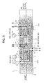
- FIG. 2 is a schematic view showing an optical RZ modulator 1 of the clock modulation type to which an optical modulator 12 - 1 according to a first embodiment of the present invention is applied.
- the optical modulator 1 shown is used, for example, with a transmission side apparatus of a long distance optical transmission system and modulates light from a light source (semiconductor laser) not shown with a transmission data signal.
- the modulated optical signal Is transmitted to the reception side through an optical fiber or the like not shown.
- the optical modulator 1 includes a Mach-Zehnder optical modulator 11 - 1 and another Mach-Zehnder optical modulator 12 - 1 according to the first embodiment integrated together with each other.
- the optical modulator 11 - 1 can modulate light from the light source not shown into an optical RZ clock of, for example, approximately 40 GHz, and the optical modulator 12 - 1 can modulate the optical RZ clock from the optical modulator 11 - 1 into an optical RZ data signal of, for example, 40 Gb/s.
- FIG. 1 is a sectional view of the optical modulator 12 - 1 taken along line R-S of FIG. 2 .
- the optical modulator 12 - 1 shown has characteristic elements of the present invention denoted by reference characters 13 - 1 and 13 - 2 in FIGS. 1 and 2. However, an overall structure of the optical modulator 1 is described first, and then the characteristic elements of the present invention are described.
- the optical modulator 1 includes a Mach-Zehnder first optical waveguide (hereinafter referred to simply as first optical waveguide) 5 , a Mach-Zehnder second optical waveguide (hereinafter referred to simply as second optical waveguide) 6 , a first electrode 7 A- 1 and a second electrode 7 B- 1 formed on a substrate 1 A, which is made of lithium niobate (LiNbO 3 ) and cut in the Z-axis direction of the crystal orientation (Z-axis cut), and integrated together in one chip.
- first optical waveguide Mach-Zehnder first optical waveguide
- second optical waveguide 6 Mach-Zehnder second optical waveguide 6
- first electrode 7 A- 1 and a second electrode 7 B- 1 formed on a substrate 1 A, which is made of lithium niobate (LiNbO 3 ) and cut in the Z-axis direction of the crystal orientation (Z-axis cut), and integrated together in one chip.
- optical waveguides 5 and 6 and the elements denoted by reference characters 13 - 1 and 13 - 2 hereinafter described are covered, at portions thereof which overlap with a grounding electrode 7 , with the grounding electrode 7 , in order to clearly indicate the arrangement of them, also the portions of them covered with the grounding electrode 7 are indicated by solid lines in FIG. 2 .
- the first optical waveguide 5 and the second optical waveguide 6 are formed integrally by thermal diffusion of titanium (Ti) or the like so that the second optical waveguide 6 may be in a relationship of cascade connection or series connection to the first optical waveguide 5 . Consequently, light from the light source is inputted from the input end of the optical modulator 1 and propagates along the first optical waveguide 5 and the second optical waveguide 6 .
- the first optical waveguide 5 includes a Y branching waveguide 5 A and two straight arm waveguides 5 B- 1 and 5 B- 2 on the light incoming side, and a Y branching waveguide 5 C on the light outgoing side.
- the second optical waveguide 6 includes a Y branching waveguide 6 A and two straight arm waveguides 6 B- 1 and 6 B- 2 on the light incoming side, and a Y branching waveguide 6 C on the light outgoing side.
- the first optical waveguide 5 is formed on the substrate 1 A such that the Y branching waveguide 5 A is branched into the two straight arm waveguides 5 B- 1 and 5 B- 2 and then the straight arm waveguides 5 B- 1 and 5 B- 2 join together at the Y branching waveguide 5 C.
- the second optical waveguide 6 is formed on the substrate 1 A such that the Y branching waveguide 6 A is branched into the two straight arm waveguides 6 B- 1 and 6 B- 2 and then the straight arm waveguides 6 B- 1 and 6 B- 2 join together at the Y branching waveguide 5 C.
- the first electrode 7 A- 1 is formed as a partial electrode layer on the substrate 1 A to control light which propagates in the first optical waveguide 5
- the second electrode 7 B- 1 is formed as a partial electrode layer on the substrate 1 A to control light which propagates in the second optical waveguide 6 .
- the first electrode 7 A- 1 includes a dual electrode having two signal electrodes 7 a - 1 and 7 a - 2 , and grounding electrodes 7 .
- the second electrode 7 B- 1 includes a signal electrode 7 b and the grounding electrodes 7 .
- the signal electrodes 7 a - 1 and 7 a - 2 of the first electrode 7 A- 1 are formed so as to establish electric connection between two connector contacts at edge portions on the opposite sides of the substrate 1 A in its widthwise direction.
- the signal electrode 7 a - 1 is formed such that part thereof extends along and above the portion at which the straight arm waveguide 5 B- 1 of the first optical waveguide 5 is formed
- the signal electrode 7 a - 2 is formed such that part thereof extends along and above the portion at which the other straight arm waveguide 5 B- 2 of the first optical waveguide 5 is formed.
- the signal electrode 7 b formed on the second optical waveguide 6 is formed so as to establish electric connection between two connector contacts at edge portions on one side of the substrate 1 A in its widthwise direction.
- the signal electrode 7 b is formed further such that part thereof extends along and above the portion at which the straight arm waveguide 6 B- 1 of the second optical waveguide 6 is formed.
- the grounding electrode 7 is formed as common grounding electrodes for the first electrode 7 A- 1 and the second electrode 7 B- 1 such that it is positioned on the opposite sides the signal electrodes 7 a - 1 , 7 a - 2 and 7 b and bias electrodes bias electrode 7 C- 1 , bias electrode 7 C- 2 and 7 D, which are hereinafter described, in a spaced relationship by a predetermined distance to form a coplanar line on the substrate 1 A.
- a connection pad 7 d is formed with a comparatively great width for an electric wiring line and serves as a connector contact for each of the signal electrodes 7 a - 1 , 7 a - 2 and 7 b described above.
- the bias electrodes bias electrode 7 C- 1 and bias electrode 7 C- 2 serve as a dual bias electrode connected to a dc power supply 7 F to supply a bias voltage to the first optical waveguide 5 to supplementarily provide an application voltage for clock modulation.
- the bias electrode bias electrode 7 C- 1 is formed such that it extends along and above a branch portion of the Y branching waveguide 5 C on the straight arm waveguide 5 B- 1 side
- the bias electrode bias electrode 7 C- 2 is formed such that it extends along and above a branch portion of the Y branching waveguide 5 C on the straight arm waveguide 5 B- 2 side.
- the bias electrode 7 D applies a dc voltage from a dc power supply 7 E as a single electrode to the second optical waveguide 6 to auxiliary provide an application voltage for NRZ optical modulation and is formed such that it extends along and above the straight arm waveguide 6 B- 1 .
- the modulation efficiency can be kept optimally by the bias voltages from the bias electrodes bias electrode 7 C- 1 , bias electrode 7 C- 2 and 7 D described above.
- bias electrodes bias electrode 7 C- 1 , bias electrode 7 C- 2 and 7 D have a connection pad 7 d similarly to the signal electrodes 7 a - 1 , 7 a - 2 and 7 b described above.
- a cutaway portion 1 B is formed at a connection path 1 C between the optical modulator 11 - 1 and the optical modulator 12 - 1 such that it cuts away the grounding electrode 7 so that the loss of light which propagates along the connection path 1 C may be reduced.
- a buffer layer (refer to reference character 1 D of FIG. 2 which is hereinafter described) is interposed between a face of the substrate 1 A and the electrode layers, and a silicon (Si) layer (refer to reference character 1 E of FIG. 2) is placed on the substrate 1 A, more particularly on the buffer layer 1 D.
- a clock generation drive section 8 A generates a sine wave signal of a frequency of, for example, 20 GHz.
- the sine wave signal of 20 GHz generated is applied through the connection pad 7 d to the signal electrode 7 a - 1 of the dual electrode.
- a phase delaying section 9 A delays a clock signal from the clock generation drive section 8 A by a time ( ⁇ ) corresponding to a predetermined phase (180 degrees) and converts the voltage of the clock signal.
- the clock signal of 20 GHz from the phase delaying section 9 A is applied through the connection pad 7 d to the other signal electrode 7 a - 2 of the dual electrode.
- the optical modulator 11 - 1 composed of the first optical waveguide 5 and the first electrode 7 A- 1 modulates light from the light source so that an optical clock signal of 40 GHz is propagated on the output side (refer to reference character C′ of FIG. 1) of the Y branching waveguide 5 C.
- the clock generation drive section 8 A and the phase delaying section 9 A described above produce, when a clock signal of a frequency (20 GHz) equal to one half the transmission rate (40 Gb/s) per unit time of output light of the optical RZ modulator 1 of the clock modulation type is applied to the first electrode 7 A- 1 , an optical RZ signal of a rate equal to the transmission rate (40 Gb/s) per unit time of the output light of the optical RZ modulator 1 of the clock modulation type.
- An NRZ data signal generator 10 is connected to the second electrode 7 B- 1 and supplies an NRZ data signal of, for example, approximately 40 Gb/s to the second electrode 7 B- 1 .
- the optical modulator 12 - 1 composed of the second optical waveguide 6 and the second electrode 7 B- 1 can modulate an optical RZ clock of 40 GHz from the first optical waveguide 5 with an NRZ data signal of 40 Gb/s at a timing synchronized with the optical RZ clock so that it can output an optical RZ data signal of 40 Gb/s.
- FIG. 1 is a sectional view taken along line R-S of the optical modulator 12 - 1 shown in FIG. 2 .
- the substrate 1 A has an electro-optical effect as described hereinabove, and is made of lithium niobate (LiNbO 3 ) and cut in the Z-axis direction of the crystal orientation (Z-axis cut).
- the substrate 1 A has formed thereon a ridge 14 a , a first groove 14 b - 1 and a second groove 14 b - 2 which are positioned on the opposite sides of the ridge 14 a , and a first bank 14 c - 1 and 14 - 2 which are positioned on the outer sides of the first groove 14 b - 1 and the second groove 14 b - 2 , respectively.
- the second arm waveguide 6 B- 2 of the second optical waveguide 6 is provided at a location of the second bank 14 c - 2 nearer to the ridge 14 a than the recess 13 - 2 which is hereinafter described.
- the second electrode 7 B- 1 is formed on the substrate 1 A for controlling light propagating in the second optical waveguide 6 and includes the signal electrode 7 b and the grounding electrodes 7 .
- the signal electrode 7 b is formed on the ridge 14 a such that the contact width We thereof with the ridge 14 a is smaller than the width Rw of the ridge 14 a .
- the grounding electrodes 7 of the second electrode 7 B- 1 is formed on the first bank 14 c - 1 and the second bank 14 c - 2 .
- the signal electrode 7 b is formed such that it has a height h 1 , but the width W 10 of the top face thereof is greater than the contact width We thereof with the ridge 14 a .
- the grounding electrodes 7 formed on the first bank 14 c - 1 and the second bank 14 c - 2 is formed with an L-shaped sectional shape taken along line R-S in FIG. 2 such that it has a height h 2 at a portion thereof adjacent an end portion of the substrate 1 A but has another height hw at a formation face thereof adjacent the ridge 14 a .
- the signal electrode 7 b is formed such that the height of the portion thereof formed with the contact width We is equal to the height hw of the formation face of the grounding electrodes 7 adjacent the ridge 14 a.
- the ridge 14 a is formed with a height Gh such that it extends in parallel to the first arm waveguide 6 B- 1 including the portion at which the first arm waveguide 6 B- 1 on which the signal electrode 7 b is placed is formed.
- the first groove 14 b - 1 and the second groove 14 b - 2 are formed by partly removing or digging the substrate 1 A to the depth Gh by etching.
- the first bank 14 c - 1 is formed by digging the first groove 14 b - 1 on the outer side of the first groove 14 b - 1 , i.e., on the outer side in the widthwise direction of the substrate 1 A
- the second bank 14 c - 2 is formed by digging the second groove 14 b - 2 on the outer side of the second groove 14 b - 2 . i.e., on the outer side in the widthwise direction of the substrate 1 A.
- the top face level of the ridge 14 a and the top face levels of the banks 14 c - 1 and 14 c - 2 are set substantially in level with each other.
- the first bank 14 c - 1 and the second bank 14 c - 2 include a first recess 13 - 1 and a second recess 13 - 2 as characteristic elements of the present invention, respectively, for reducing the loss in the waveguide and suppressing the loss of a microwave which advances in the signal electrode 7 b.
- the first recess 13 - 1 and the second recess 13 - 2 are set to a depth Gh substantially equal to that of the first groove 14 b - 1 and the second groove 14 b - 2 and are formed at symmetrical positions with respect to the ridge 14 a in the first bank 14 c - 1 and the second bank 14 c - 2 , respectively, using etching.
- first recess 13 - 1 and the second recess 13 - 2 can be formed in a shape of a continuous groove of the width Gw 2 such that they may extend in parallel to the first arm waveguide 6 B- 1 and the second arm waveguide 6 B- 2 and have a length substantially equal to the length L of the grounding electrodes 7 on the upper face of the second arm waveguide 6 B- 2 as indicated by broken lines in FIG. 2 .
- the two recesses 13 - 1 and 13 - 2 described above can be formed such that they have a symmetrical relationship with respect to the line of the first arm waveguide 6 b- 1 which has the signal electrode 7 b formed on the upper face thereof.
- the grounding electrodes 7 is formed also on the recesses 13 - 1 and 13 - 2 , and an air gap is formed in each of the recesses 13 - 1 and 13 - 2 , that is, a region defined by each of the recesses 13 - 1 and 13 - 2 and the grounding electrodes 7 .
- the buffer layer 1 D is provided for suppressing the absorption loss of light which propagates in the optical waveguides 5 and 6 and is formed between the electrodes 7 A- 1 and 7 B- 1 , which form the optical modulators 11 - 1 and 12 - 1 , respectively, and the substrate 1 A.
- a silicon layer 1 E is formed on the substrate 1 A, particularly on the buffer layer 1 D.
- the silicon layer 1 E is effective to uniformize electric charge generated by a pyroelectric effect to suppress a variation of the operating point by a temperature variation.
- the buffer layer 1 D and the silicon layer 1 E are provided also in the recesses 13 - 1 and 13 - 2 and facilitate adjustment of the characteristic impedance, which should be kept to a fixed value set in advance, and the velocity match between a microwave and light by setting of the thickness of the buffer layer 1 D and the silicon layer 1 E.
- an NRZ signal of 40 Gb/s generated by the NRZ data signal generator 10 is applied to the second electrode 7 B- 1 to modulate the optical clock thereby to modulate the optical RZ signal into an optical RZ data signal of 40 Gb/s.
- the optical RZ data signal is transmitted to the reception side through an optical fiber or the like not shown.
- the structure of the portion at which the second arm waveguide 6 B- 2 is formed can be formed substantially same as the structure of the ridge 14 a which has the signal electrode 7 b provided on the top portion thereof. Consequently, the losses by the arm waveguides 6 B- 1 and 6 B- 2 are substantially equal to each other.
- the electric field distribution in the substrate 1 A by an electric signal provided to the signal electrode 7 b can be made symmetrical with respect to the ridge 14 a.
- the optical modulator 12 - 1 since the first recess 13 - 1 and the second recess 13 - 2 are formed at symmetrical positions with respect to the ridge 14 a on the first bank 14 c - 1 and the second bank 14 c - 2 , respectively, also the electric field distribution in the substrate 1 A by an electric signal provided to the signal electrode 7 b can be made symmetrical with respect to the ridge 14 a . Consequently, the optical modulator 12 - 1 is advantageous in that the loss of a microwave which advances in the signal electrode 7 b can be suppressed.
- the optical modulator 12 - 1 is advantageous also in that the losses by the arm waveguides 6 B- 1 and 6 B- 2 can be made substantially equal to each other thereby to suppress the deterioration of the extinction ratio.
- the optical modulator 12 - 1 is further advantageous in that the absolution losses of light which propagates in the optical waveguides 5 and 6 can be suppressed and electric charge generated by a pyroelectric effect can be made uniform by the silicon layer 1 E formed on the substrate 1 A thereby to suppress the variation of the operating point by a temperature variation.
- the optical modulator 12 - 1 is advantageous in that adjustment of the characteristic impedance, which should be kept to a fixed value set in advance, and the velocity match between a microwave and light can be performed readily by setting of the thickness of the buffer layer 1 D.
- FIG. 3 is a schematic view showing an optical RZ modulator of the clock modulation type to which optical modulators 11 - 2 and 12 - 1 according to a second embodiment of the present invention are applied.
- the optical RZ modulator 2 of the clock modulation type shown in FIG. 3 is common to that of the first embodiment described hereinabove in that two kinds of Mach-Zehnder optical modulators are formed integrally on the substrate 1 A made of lithiumniobate (LiNbO 3 ) and Z-axis cut, but is different in configuration of the first Mach-Zehnder optical modulator 11 - 2 .
- the second Mach-Zehnder optical modulator 12 - 1 is configured in a similar manner to that in the first embodiment described hereinabove.
- the first Mach-Zehnder optical modulator 11 - 2 includes a first electrode 7 A- 2 and a bias electrode 7 C different from those of the first Mach-Zehnder optical modulator 11 - 1 in the first embodiment, and includes characteristic elements (refer to reference characters 13 - 1 and 13 - 2 ) of the present embodiment similar to those in the Mach-Zehnder optical modulator 12 - 1 .
- the first electrode 7 A- 2 includes a single signal electrode 7 a and the grounding electrodes 7 .
- the signal electrode 7 a is formed so as to establish electric connection between two connector contacts at edge portions of one side of the substrate 1 A in its widthwise direction similarly to the signal electrode 7 b of the second Mach-Zehnder optical modulator 12 - 1 .
- the signal electrode 7 a is formed further such that part thereof extends along and above the portion at which the straight arm waveguide 5 B- 1 of the first optical waveguide 5 is formed.
- the first electrode 7 A- 2 and the second electrode 7 B- 1 are each formed as a single electrode having the single signal electrode 7 a or 7 b.
- first electrode 7 A- 2 and the second electrode 7 B- 1 in the second embodiment include the single signal electrodes. 7 a and 7 b , respectively, the second embodiment need not include a phase delaying section (reference character 9 A of FIG. 1) for applying a clock signal voltage to the dual electrode like the first electrode 7 A- 1 in the first embodiment.
- the bias electrode 7 C applies a dc voltage from the dc power supply 7 F as a single electrode to the first optical waveguide 5 and is formed such that it extends along and above the straight arm waveguide 5 B- 1 .
- the bias electrode 7 C described above includes a connection pad 7 d similarly to the bias electrode 7 D of the second Mach-Zehnder optical modulator 12 - 1 .
- the optical modulator 11 - 2 includes a first recess 13 - 1 and a second recess 13 - 2 as characteristic elements of the present invention for reducing the loss by the waveguide and suppressing the loss of a microwave which advances through the signal electrode 7 a similarly as in the optical modulator 12 - 1 .
- the sectional structure of the optical modulator 11 - 2 taken along line R-S in FIG. 3 is basically similar to that described hereinabove with reference to FIG. 1 except that the signal electrode 7 a is formed on the ridge 14 a.
- the optical modulator 2 in the second embodiment is formed from two optical modulators 11 - 2 and 12 - 1 respectively having the recesses 13 - 1 and 13 - 2 , which are characteristic elements of the present invention, and integrated integrally on one chip.
- optical modulator 2 in the second embodiment having the configuration described above, when light from the light source not shown is introduced into it, while the light propagates in the first optical waveguide 5 which forms the optical modulator 11 - 2 , it can be converted into an optical RZ signal of 40 GHz with a sine wave of 20 GHz by the first electrode 7 A- 2 to which an RZ signal of a frequency of 20 GHz generated by the clock generation drive section 8 A is applied.
- an NRZ signal of 40 Gb/s generated by the NRZ data signal generator 10 is applied to the second electrode 7 B- 1 to modulate the optical clock thereby to modulate the optical RZ signal into an optical RZ data signal of 40 Gb/s.
- the optical RZ data signal is transmitted to the reception side through an optical fiber or the like not shown.
- the structures of the portions at which the second arm waveguides 5 B- 2 and 6 B- 2 are formed can be formed substantially same as the structure of the ridges 14 a which has the signal electrodes 7 a and 7 b provided on the tops thereof. Consequently, the losses by the arm waveguides 5 B- 1 , 5 B- 2 . 6 B- 1 and 6 B- 2 are substantially equal to each other.
- the electric field distribution in the substrate 1 A by electric signals provided to the signal electrodes 7 a and 7 b can be made symmetrical with respect to the ridge 14 a.
- the optical modulators 11 - 2 and 12 - 1 since the first recess 13 - 1 and the second recess 13 - 2 are formed at symmetrical positions with respect to the ridge 14 a on the first bank 14 c - 1 and the second bank 14 c - 2 , respectively, also the electric field distribution in the substrate 1 A by an electric signal provided to the signal electrode 7 b can be made symmetrical with respect to the ridge 14 a similarly as in the first embodiment described hereinabove. Consequently, the optical modulators 11 - 2 and 12 - 1 are advantageous in that the loss of a microwave which advances in the signal electrodes 7 a and 7 b can be suppressed.
- the optical modulators 11 - 2 and 12 - 1 are advantageous also in that the losses by the arm waveguides 5 B- 1 , 5 B- 2 , 6 B- 1 and 6 B- 2 can be made substantially equal to each other thereby to suppress the deterioration of the extinction ratio.
- the optical modulators 11 - 2 and 12 - 1 are further advantageous in that the absorption losses of light which propagates in the optical waveguides 5 and 6 can be suppressed and electric charge generated by a pyroelectric effect can be made uniform by the silicon layer 1 E thereby to suppress the variation of the operating point by a temperature variation.
- the buffer layer 1 D and the silicon layer 1 E are formed also in the recesses 13 - 1 and 13 - 2 , adjustment of the characteristic impedance, which should be kept to a fixed value set in advance, and the velocity match between a microwave and light can be performed readily by setting of the thickness of the buffer layer ID and the silicon layer 1 E.
- FIG. 4 is a schematic view showing an optical RZ modulator of the clock modulation type to which an optical modulator 11 - 2 according to a third embodiment of the present invention is applied.
- the optical RZ modulator 3 of the clock modulation type shown in FIG. 4 is common to those of the first and second embodiments described hereinabove in that two kinds of Mach-Zehnder optical modulators are formed integrally on the substrate 1 A made of lithium niobate (LiNbO 3 ) and Z-axis cut, but is different in configuration of a second Mach-Zehnder optical modulator 12 - 2 .
- first Mach-Zehnder optical modulator 11 - 2 having recesses 13 - 1 and 13 - 2 which are characteristic elements of the present invention is configured in a similar manner to that in the second embodiment described hereinabove.
- optical waveguides 5 and 6 and the elements denoted by reference characters 13 - 1 and 13 - 2 which are hereinafter described are indicated, at portions thereof which are covered with grounding electrodes 7 , by solid lines in FIG. 4 .
- the second Mach-Zehnder optical modulator 12 - 2 includes a second electrode 7 B- 2 and bias electrodes 7 D- 1 and 7 D- 2 different from those of the second Mach-Zehnder optical modulator 12 - 1 in the first and second embodiments, but does not include recesses as characteristic elements of the present invention.
- the second electrode 7 B- 2 is formed on the substrate 1 A for controlling light which propagates in the second optical waveguide 6 and includes a dual electrode having two signal electrodes 7 b - 1 and 7 b - 2 and grounding electrodes 7 .
- the signal electrodes 7 b - 1 and 7 b - 2 are formed so as to establish electric connection between two connector contacts at edge portions of the opposite sides of the substrate 1 A in its widthwise direction.
- the signal electrode 7 b - 1 is formed such that part thereof extends along and above the portion at which the straight arm waveguide 6 B- 1 of the second optical waveguide 6 is formed.
- The, signal electrode 7 b - 2 is formed such that part thereof extends along and above the portion at which the other straight arm waveguide 6 B- 2 of the second optical waveguide 6 is formed.
- the second electrode 7 B- 2 is formed as a dual electrode having two signal electrodes while the first electrode 7 A- 2 is formed as a single electrode having a single signal electrode.
- NRZ data signal generators 10 - 1 and 10 - 2 are connected to the signal electrodes 7 b - 1 and 7 b - 2 of the second electrode 7 B- 1 and supply NRZ data signals of a bit rate corresponding to an optical clock to the second electrode 7 B- 2 .
- the NRZ data signal generators 10 - 1 and 10 - 2 generate same NRZ data signals having phases displaced by 180 degrees from each other.
- the NRZ data signal voltage from the NRZ data generator 10 - 1 is applied to the signal electrode 7 b - 1
- the NRZ data signal voltage from the NRZ data generator 10 - 2 is applied to the signal electrode 7 b - 2 .
- the NRZ data signal generators 10 - 1 and 10 - 2 are shown such that they generate data signals of 40 Gb/s.
- optical modulator 3 of the third embodiment having the configuration described above, when light from the light source not shown is introduced into it, while the light propagates in the first optical waveguide 5 which forms the optical modulator 11 - 2 , it can be converted into an optical RZ signal of 40 GHz with a sine wave of 20 GHz by the first electrode 7 A- 2 to which an RZ signal of a frequency of 20 GHz generated by the clock generation drive section 8 A is applied.
- optical RZ signal propagates in the second optical waveguide 6 which forms the optical modulator 12 - 2
- NRZ signals of 40 Gb/s generated by the NRZ data signal generators 10 - 1 and 10 - 2 are applied to the signal electrodes 7 b - 1 and 7 b - 2 of the second electrode 7 B- 1 , respectively, to modulate the optical clock thereby to modulate the optical RZ signal into an optical RZ data signal of 40 Gb/s.
- the optical RZ data signal is transmitted to the reception side through an optical fiber or the like not shown.
- the structure of the portion at which the second arm waveguide 5 B- 2 is formed can be formed substantially same as the structure of the ridge 14 a which has the signal electrode 7 a provided on the top portion thereof. Consequently, the losses by the arm waveguides 5 B- 1 and 5 B- 2 are substantially equal to each other.
- the electric field distribution in the substrate 1 A by electric signals provided to the signal electrodes 7 a and 7 b can be made symmetrical with respect to the ridge 14 a.
- the optical modulator 11 - 2 is formed integrally and the first recess 13 - 1 and the second recess 13 - 2 are formed at symmetrical positions with respect to the ridge 14 a on the first bank 14 c - 1 and the second bank 14 c - 2 , respectively, similar advantages to those of the first embodiment described hereinabove can be achieved.
- the optical modulator 3 is further advantageous in that the absorption losses of light which propagates in the optical waveguides 5 and 6 can be suppressed and electric charge generated by a pyroelectric effect can be made uniform by the silicon layer 1 E thereby to suppress the variation of the operating point by a temperature variation.
- the buffer layer 1 D and the silicon layer 1 E are formed also in the recesses 13 - 1 and 13 - 2 , adjustment of the characteristic impedance, which should be kept to a fixed value set in advance, and the velocity match between a microwave and light can be performed readily by setting of the thickness of the buffer layer 1 D and the silicon layer 1 E.
- an optical modulator having the recesses 13 - 1 and 13 - 2 which are characteristic elements of the present invention is applied to an optical RZ modulator of the clock modulation type.
- an optical modulator it is naturally possible, for example, to form an optical modulator as a single drive optical modulator 12 of a single unit having a basically similar configuration to that of the optical modulators 11 - 2 and 12 - 1 of the first to third embodiments described hereinabove, as shown in FIG. 5
- the optical modulator 12 according to the fourth embodiment can be used as a single drive modulator which performs NRZ data modulation of light from a light source similarly to the optical modulator 20 described hereinabove with reference to FIG. 8 .
- the optical modulator 12 is different from the optical modulator 20 in that it has recesses 13 - 1 and 13 - 2 which are characteristic elements of the present invention.
- optical waveguide 6 and the elements denoted by reference characters 13 - 1 and 13 - 2 are indicated, at portions thereof which are covered with a grounding electrode 7 , by solid lines in FIG. 5 .
- the sectional structure taken along line R-S of FIG. 5 is configured basically similarly to that described hereinabove with reference to FIG. 1 . Consequently, the optical modulator 12 can reduce the loss of the waveguide and suppress the loss of a microwave which advances in the signal electrode 7 b . It is to be noted that, in FIG. 4, like reference characters similar to those of FIG. 1 denote substantially like elements.
- the single drive optical modulator 12 having the configuration described above with reference to FIG. 4, when light from the light source not shown is introduced into it, while the light propagates in the Mach-Zehnder optical waveguide, it is modulated into an NRZ optical signal by the signal electrode 7 b to which a voltage signal of NRZ data or the like is applied.
- the NRZ optical signal is outputted from the single drive optical modulator 12 .
- the structure of the portion at which the second arm waveguide 6 B- 2 is formed can be formed substantially same as the structure of the ridge 14 a which has the signal electrode 7 b provided at the top portion thereof. Consequently, the losses by the straight arm waveguides 6 B- 1 and 6 B- 2 are substantially equal to each other.
- the electric field distribution in the substrate 1 A by an electric signal provided to the signal electrode 7 b can be made symmetrical with respect to the ridge 14 a.
- the optical modulator according to the present invention is not limited to the specific configuration and may otherwise be configured such that, for example, as shown in FIG. 6, a grounding electrode 7 is provided above each of the first recess 13 - 1 and the second recess 13 - 2 and part of the grounding electrode 7 is filled in each of the first recess 13 - 1 and the second recess 13 - 2 .
- the buffer layer 1 D is formed between the substrate 1 A and the first electrode 7 A- 1 and second electrode 7 B- 1 and the silicon layer 1 E is formed on the buffer layer 1 D over the overall area of the substrate 1 A (refer to FIG. 1 ), according to the present invention, it is otherwise possible to configure the optical modulator such that, for example, as shown in a cross sectional view of FIG. 7 taken along line R-S, a buffer layer 1 D′ and a silicon layer 1 E are formed between at least the portions of the substrate 1 A on which the optical waveguides 5 and 6 are formed and the first electrode 7 A- 1 and second electrode 7 B- 1 . Also where the optical modulator is configured in this manner, at least the absorption losses of light which propagates in the optical waveguides 5 and 6 can be suppressed.
- the modulators of the embodiments described above in which the recesses 13 - 1 and 13 - 2 are provided are shown such that the width of the first arm waveguides 5 B- 1 and 6 B- 1 is substantially equal to the contact width of the signal electrode 7 b with the ridge 14 a
- the relationship of the width Rw of the ridge 14 a , the waveguide width and the contact width We between the signal electrode 7 b and the ridge 14 a can be varied within a range within which the balance among the demand for suppression of the waveguide loss, the demand for lowering of the drive voltage and the demand for the velocity match between microwave and light can be maintained taking the electrode distance Se and the electrode thickness into consideration.
- the recesses 13 - 1 and 13 - 2 are each formed in a shape of a continuous groove such that they extend in parallel to the first arm waveguides 5 B- 1 and 6 B- 1 and the second arm waveguides 5 B- 2 and 6 B- 2 and have a length substantially equal to the length L of the grounding electrode 7 on the upper faces of the second arm waveguide 5 B- 2 and 6 B- 2 , similar advantages to those which can be achieved by the embodiments described hereinabove can be achieved even where the optical modulator is formed such that the length of the continuous groove shape of the recesses 13 - 1 and 13 - 2 is varied or each of the recesses 13 - 1 and 13 - 2 has a shape of an intermittent groove.
- optical modulates of the embodiments described above can modulate a data signal into an optical signal having an information amount of 40 Gb/s
- the present invention can be applied to another optical modulator for modulation into an optical signal having an information amount smaller than 40 Gb/s or a further optical modulator for modulation into an optical signal having an information amount greater than 40 Gb/s.
Landscapes
- Physics & Mathematics (AREA)
- Nonlinear Science (AREA)
- Electromagnetism (AREA)
- General Physics & Mathematics (AREA)
- Optics & Photonics (AREA)
- Optical Modulation, Optical Deflection, Nonlinear Optics, Optical Demodulation, Optical Logic Elements (AREA)
Abstract
The invention provides an optical modulator which suppresses the loss of a microwave which advances through an electrode and of light which propagates in a waveguide and makes the losses in individual arm waveguides substantially equal to each other to suppress the deterioration of the extinction coefficient to improve the transmission quality. The optical modulator includes a substrate having an electro-optical effect and having a ridge, first and second grooves and first and second banks formed thereon, a Mach-Zehnder optical waveguide, an electrode, and first and second recesses formed at symmetrical positions with respect to the ridge on the first and second banks, respectively. The optical modulator is applied, for example, to a transmission side apparatus for a long distance optical transmission system.
Description
This application is a divisional of application Ser. No. 09/820,634, filed Mar. 30, 2001, now U.S. Pat. No. 6,584,240.
1) Field of the Invention
This invention relates to an optical modulator suitable for use in the field of long distance optical communication systems.
2) Description of the Related Art
As the data transmission rate increases in recent years, optical modulators for modulating a data signal from an electric signal into an optical signal are developed energetically in the field of long distance communication systems for communication such as submarine optical communication.
One of such optical modulators as just described is, for example, such a single drive optical modulator 20 as shown in FIG. 8. Referring to FIG. 8, the single drive optical modulator 20 shown includes a substrate 21 on which a Mach-Zehnder optical waveguide 22 is formed, and an electrode 23 formed integrally on the substrate 21 and including a single signal electrode 23A and a grounding electrode 23B.
FIG. 9 is a sectional view taken along line A-A′ of the single electrode optical modulator 20 shown in FIG. 8. As seen in FIG. 9, the single electrode optical modulator 20 is configured such that the electrode 23 is formed on the substrate 21, which is made of, for example, lithium niobate (LiNbO3) and cut (Z-axis cut) in the Z-axis direction of the crystal orientation, together with the Mach-Zehnder optical waveguide 22.
The Mach-Zehnder optical waveguide 22 is formed by thermal diffusion of titanium (Ti) or a like substance on the substrate 21 and includes a Y branching waveguide 22A and two straight arm waveguides 22B-1 and 22B-2 on the light incoming side and a Y branching waveguide 22C on the light outgoing side. The electrode 23 includes the single signal electrode 23A and the grounding electrode 23B and converts, when a voltage signal (microwave) of, for example, NRZ data or the like is applied to the signal electrode 23A, the voltage signal into an NRZ optical signal.
As shown in FIG. 8, the single signal electrode 23A is formed so as to establish electric connection between two connector contacts on a one-side edge portion of the substrate 21 in its widthwise direction, and is formed such that part of it extends along and above the portion at which the straight arm waveguide 22B-1 is formed. Further, the grounding electrode 23B is formed such that it is disposed on the opposite sides of the single signal electrode in a spaced relationship by a predetermined distance thereby to form a coplanar line on the substrate 21.
When light from a light source not shown is introduced into the single electrode optical modulator 20 having the configuration described above with reference to FIGS. 8 and 9, while the light propagates in the Mach-Zehnder optical waveguide 22, it is modulated into an NRZ optical signal by the signal electrode 23A to which a voltage signal (microwave) of NRZ data or the like is applied. The modulated NRZ optical signal goes out of the single electrode optical modulator 20.
Where such a single electrode optical modulator 20 as described above is used to modulate a voltage signal into a data optical signal of a transmission rate particularly of 10 Gb/s or more, preferably of approximately 40 Gb/s, it is a significant subject for improvement of the transmission quality to suppress the loss of a microwave which advances through the electrode and suppress the deterioration of the extinction ratio.
It is an object of the present invention to provide an optical modulator which suppresses the loss of a microwave which advances through an electrode and loss of light which propagates in a waveguide and makes the losses in individual arm waveguides substantially equal to each other to suppress the deterioration of the extinction ratio to improve the transmission quality.
In order to attain the object described above, according to an aspect of the present invention, there is provided an optical modulator, comprising a substrate having an electro-optical effect and having formed thereon a ridge, first and second grooves which are positioned on the opposite sides of the ridge, and first and second banks which are positioned on the outer sides of the first and second grooves, respectively, a Mach-Zehnder optical waveguide formed on the substrate and including a first Y branching waveguide, first and second arm waveguides which are branched from the first Y branching waveguide and one of which is included in the ridge, and a second Y branching waveguide at which the first and second arm waveguides join together, an electrode formed on the substrate and including a signal electrode formed on the ridge and a grounding electrode formed on the first and second banks for controlling light propagating in the optical waveguide, and first and second recesses formed at symmetrical positions with respect to the ridge on the first and second banks, respectively.
With the optical modulator, since the first and second recesses are formed at the symmetrical positions with respect to the ridge 14 a on the first and second banks, respectively, also the electric field distribution in the substrate by an electric signal provided to the signal electrode can be made symmetrical with respect to the ridge. Consequently, the optical modulator is advantageous in that the loss of a microwave which advances through the signal electrode can be suppressed.
Preferably, the substrate is made of LiNbO3, and more preferably, the substrate made of LiNbO3 is a Z-axis cut substrate.
The optical modulator may be configured such that the grounding electrode is provided on the first and second recesses and an air gap is formed in each of the first and second recesses or part of the grounding electrode is filled in the first and second recesses.
Preferably, the ridge and the first and second banks have top faces which are set in a substantially same level with one another, and more preferably, the first and second recesses have a depth set substantially equal to the depth of the first and second grooves.
Preferably, the signal electrode contacts with the ridge with a width smaller than the width of the ridge.
Preferably, a buffer layer is formed between the substrate and the electrode, and more preferably, the buffer layer is provided also in the first and second recesses.
Preferably, a silicon layer is placed on the substrate, and more preferably, the buffer layer is provided also in the first and second recesses.
The optical modulator is advantageous in that the absorption loss of light which propagates in the optical waveguide can be suppressed by the buffer layer and electric charge generated by a pyroelectric effect can be made uniform by the silicon layer to suppress the variation of the operating point by a temperature variation.
Further, since the buffer layer or the silicon layer is formed also in the first and second recesses 13-1, 13-2, the optical modulator is advantageous also in that adjustment of the characteristic impedance, which should be kept to a fixed value set in advance, and the speed matching between a microwave and light can be performed readily by setting of the thickness of the buffer layer or the silicon layer.
Preferably, one of the first and second arm waveguides is provided at a location of the other one of the first and second banks nearer to the ridge than a corresponding one of the first and second recesses.
With the optical modulator, since the one arm waveguide is provided nearer to the ridge than the other recess, the structure of the substrate portion at which the arm waveguide which is not included in the ridge is formed can be formed substantially same as the structure of the ridge. Therefore, the optical modulator is advantageous in that the losses of the arm waveguides can be made substantially equal to each other to suppress the deterioration of the extinction ratio.
According to another aspect of the present invention, there is provided an optical modulator, comprising a Z-axis cut substrate made of LiNbO3 and having formed thereon a ridge, first and second grooves which are positioned on the opposite sides of the ridge, and first and second banks which are positioned on the outer sides of the first and second grooves, respectively, a Mach-Zehnder optical waveguide formed on the substrate and including a first Y branching waveguide, first and second arm waveguides which are branched from the first Y branching waveguide and one of which is included in the ridge, and a second Y branching waveguide at which the first and second arm waveguides join together, an electrode formed on the substrate and including a signal electrode formed on the ridge and a grounding electrode formed on the first and second banks for controlling light propagating in the optical waveguide, a buffer layer formed between the substrate and the electrode, a silicon layer placed on the substrate, and first and second recesses formed at symmetrical positions with respect to the ridge on the first and second banks, respectively.
With the optical modulator, since the first and second recesses are formed at the symmetrical positions with respect to the ridge 14 a on the first and second banks, respectively, also the electric field distribution in the substrate by an electric signal provided to the signal electrode can be made symmetrical with respect to the ridge. Consequently, the optical modulator is advantageous in that the loss of a microwave which advances through the signal electrode can be suppressed.
Preferably, the buffer layer or the silicon layer is provided also in the first and second recesses. In this instance, the optical modulator is advantageous also in that adjustment of the characteristic impedance, which should be kept to a fixed value set in advance, and the velocity match between a microwave and light can be performed readily by setting of the thickness of the buffer layer or the silicon layer.
Preferably, one of the first and second arm waveguides is provided at a location of the other one of the first and second banks nearer to the ridge than a corresponding one of the first and second recesses. In this instance, the structure of the substrate portion at which the arm waveguide which is not included in the ridge is formed can be formed substantially same as the structure of the ridge. Therefore, the optical modulator is advantageous in that the losses of the arm waveguides can be made substantially equal to each other to suppress the deterioration of the extinction ratio.
The above and other objects, features and advantages of the present invention will become apparent from the following description and the appended claims, taken in conjunction with the accompanying drawings.
FIG. 1 is a schematic view showing a cross sectional structure of an optical modulator according to several embodiments of the present invention;
FIG. 2 is a schematic view showing an optical modulator according to a first embodiment of the present invention;
FIG. 3 is a schematic view showing an optical modulator according to a second embodiment of the present invention;
FIG. 4 is a schematic view showing an optical modulator according to a third embodiment of the present invention;
FIG. 5 is a schematic view showing an optical modulator according to a fourth embodiment of the present invention;
FIGS. 6 and 7 are schematic views showing optical modulators according to different modifications to the embodiments;
FIG. 8 is a schematic view showing a single drive optical modulator; and
FIG. 9 is a sectional view taken along line A-A′ of the optical modulator shown in FIG. 8.
The embodiments of the present invention will be explained referring to the accompanying drawings.
FIG. 2 is a schematic view showing an optical RZ modulator 1 of the clock modulation type to which an optical modulator 12-1 according to a first embodiment of the present invention is applied. Referring to FIG. 2, the optical modulator 1 shown is used, for example, with a transmission side apparatus of a long distance optical transmission system and modulates light from a light source (semiconductor laser) not shown with a transmission data signal. The modulated optical signal Is transmitted to the reception side through an optical fiber or the like not shown.
The optical modulator 1 includes a Mach-Zehnder optical modulator 11-1 and another Mach-Zehnder optical modulator 12-1 according to the first embodiment integrated together with each other. The optical modulator 11-1 can modulate light from the light source not shown into an optical RZ clock of, for example, approximately 40 GHz, and the optical modulator 12-1 can modulate the optical RZ clock from the optical modulator 11-1 into an optical RZ data signal of, for example, 40 Gb/s.
FIG. 1 is a sectional view of the optical modulator 12-1 taken along line R-S of FIG. 2. The optical modulator 12-1 shown has characteristic elements of the present invention denoted by reference characters 13-1 and 13-2 in FIGS. 1 and 2. However, an overall structure of the optical modulator 1 is described first, and then the characteristic elements of the present invention are described.
Referring to FIG. 2, the optical modulator 1 includes a Mach-Zehnder first optical waveguide (hereinafter referred to simply as first optical waveguide) 5, a Mach-Zehnder second optical waveguide (hereinafter referred to simply as second optical waveguide) 6, a first electrode 7A-1 and a second electrode 7B-1 formed on a substrate 1A, which is made of lithium niobate (LiNbO3) and cut in the Z-axis direction of the crystal orientation (Z-axis cut), and integrated together in one chip.
It is to be noted that, while the optical waveguides 5 and 6 and the elements denoted by reference characters 13-1 and 13-2 hereinafter described are covered, at portions thereof which overlap with a grounding electrode 7, with the grounding electrode 7, in order to clearly indicate the arrangement of them, also the portions of them covered with the grounding electrode 7 are indicated by solid lines in FIG. 2.
The first optical waveguide 5 and the second optical waveguide 6 are formed integrally by thermal diffusion of titanium (Ti) or the like so that the second optical waveguide 6 may be in a relationship of cascade connection or series connection to the first optical waveguide 5. Consequently, light from the light source is inputted from the input end of the optical modulator 1 and propagates along the first optical waveguide 5 and the second optical waveguide 6.
The first optical waveguide 5 includes a Y branching waveguide 5A and two straight arm waveguides 5B-1 and 5B-2 on the light incoming side, and a Y branching waveguide 5C on the light outgoing side. Similarly, the second optical waveguide 6 includes a Y branching waveguide 6A and two straight arm waveguides 6B-1 and 6B-2 on the light incoming side, and a Y branching waveguide 6C on the light outgoing side.
In particular, the first optical waveguide 5 is formed on the substrate 1A such that the Y branching waveguide 5A is branched into the two straight arm waveguides 5B-1 and 5B-2 and then the straight arm waveguides 5B-1 and 5B-2 join together at the Y branching waveguide 5C. The second optical waveguide 6 is formed on the substrate 1A such that the Y branching waveguide 6A is branched into the two straight arm waveguides 6B-1 and 6B-2 and then the straight arm waveguides 6B-1 and 6B-2 join together at the Y branching waveguide 5C.
The first electrode 7A-1 is formed as a partial electrode layer on the substrate 1A to control light which propagates in the first optical waveguide 5, and the second electrode 7B-1 is formed as a partial electrode layer on the substrate 1A to control light which propagates in the second optical waveguide 6.
The first electrode 7A-1 includes a dual electrode having two signal electrodes 7 a-1 and 7 a-2, and grounding electrodes 7. The second electrode 7B-1 includes a signal electrode 7 b and the grounding electrodes 7.
The signal electrodes 7 a-1 and 7 a-2 of the first electrode 7A-1 are formed so as to establish electric connection between two connector contacts at edge portions on the opposite sides of the substrate 1A in its widthwise direction. The signal electrode 7 a-1 is formed such that part thereof extends along and above the portion at which the straight arm waveguide 5B-1 of the first optical waveguide 5 is formed, and the signal electrode 7 a-2 is formed such that part thereof extends along and above the portion at which the other straight arm waveguide 5B-2 of the first optical waveguide 5 is formed.
The signal electrode 7 b formed on the second optical waveguide 6 is formed so as to establish electric connection between two connector contacts at edge portions on one side of the substrate 1A in its widthwise direction. The signal electrode 7 b is formed further such that part thereof extends along and above the portion at which the straight arm waveguide 6B-1 of the second optical waveguide 6 is formed.
The grounding electrode 7 is formed as common grounding electrodes for the first electrode 7A-1 and the second electrode 7B-1 such that it is positioned on the opposite sides the signal electrodes 7 a-1, 7 a-2 and 7 b and bias electrodes bias electrode 7C-1, bias electrode 7C-2 and 7D, which are hereinafter described, in a spaced relationship by a predetermined distance to form a coplanar line on the substrate 1A.
A connection pad 7 d is formed with a comparatively great width for an electric wiring line and serves as a connector contact for each of the signal electrodes 7 a-1, 7 a-2 and 7 b described above. The bias electrodes bias electrode 7C-1 and bias electrode 7C-2 serve as a dual bias electrode connected to a dc power supply 7F to supply a bias voltage to the first optical waveguide 5 to supplementarily provide an application voltage for clock modulation.
The bias electrode bias electrode 7C-1 is formed such that it extends along and above a branch portion of the Y branching waveguide 5C on the straight arm waveguide 5B-1 side, and the bias electrode bias electrode 7C-2 is formed such that it extends along and above a branch portion of the Y branching waveguide 5C on the straight arm waveguide 5B-2 side. The bias electrode 7D applies a dc voltage from a dc power supply 7E as a single electrode to the second optical waveguide 6 to auxiliary provide an application voltage for NRZ optical modulation and is formed such that it extends along and above the straight arm waveguide 6B-1.
It is to be noted that, also when the modulation characteristic is varied by a temperature variation or the like, the modulation efficiency can be kept optimally by the bias voltages from the bias electrodes bias electrode 7C-1, bias electrode 7C-2 and 7D described above.
Also the bias electrodes bias electrode 7C-1, bias electrode 7C-2 and 7D have a connection pad 7 d similarly to the signal electrodes 7 a-1, 7 a-2 and 7 b described above.
A cutaway portion 1B is formed at a connection path 1C between the optical modulator 11-1 and the optical modulator 12-1 such that it cuts away the grounding electrode 7 so that the loss of light which propagates along the connection path 1C may be reduced.
In the optical modulator 1 according to the first embodiment, a buffer layer (refer to reference character 1D of FIG. 2 which is hereinafter described) is interposed between a face of the substrate 1A and the electrode layers, and a silicon (Si) layer (refer to reference character 1E of FIG. 2) is placed on the substrate 1A, more particularly on the buffer layer 1D.
A clock generation drive section 8A generates a sine wave signal of a frequency of, for example, 20 GHz. The sine wave signal of 20 GHz generated is applied through the connection pad 7 d to the signal electrode 7 a-1 of the dual electrode.
A phase delaying section 9A delays a clock signal from the clock generation drive section 8A by a time (τ) corresponding to a predetermined phase (180 degrees) and converts the voltage of the clock signal. The clock signal of 20 GHz from the phase delaying section 9A is applied through the connection pad 7 d to the other signal electrode 7 a-2 of the dual electrode.
Consequently, the optical modulator 11-1 composed of the first optical waveguide 5 and the first electrode 7A-1 modulates light from the light source so that an optical clock signal of 40 GHz is propagated on the output side (refer to reference character C′ of FIG. 1) of the Y branching waveguide 5C.
In particular, the clock generation drive section 8A and the phase delaying section 9A described above produce, when a clock signal of a frequency (20 GHz) equal to one half the transmission rate (40 Gb/s) per unit time of output light of the optical RZ modulator 1 of the clock modulation type is applied to the first electrode 7A-1, an optical RZ signal of a rate equal to the transmission rate (40 Gb/s) per unit time of the output light of the optical RZ modulator 1 of the clock modulation type.
In other words, light which propagates in the straight arm waveguides 5B-1 and 5B-2 of the first optical waveguide 5 is acted upon by an electro-optical effect of an electric signal as a clock signal applied to the first electrode 7A-1 so that an optical RZ clock of 40 GHz can be produced on the output side 5C′ of the Y branching waveguide 5C.
An NRZ data signal generator 10 is connected to the second electrode 7B-1 and supplies an NRZ data signal of, for example, approximately 40 Gb/s to the second electrode 7B-1.
In particular, the optical modulator 12-1 composed of the second optical waveguide 6 and the second electrode 7B-1 can modulate an optical RZ clock of 40 GHz from the first optical waveguide 5 with an NRZ data signal of 40 Gb/s at a timing synchronized with the optical RZ clock so that it can output an optical RZ data signal of 40 Gb/s.
More particularly, light which propagates in the straight arm waveguide 6B-1 of the second optical waveguide 6 is acted upon by an electro-optical effect of an electric signal applied to the second electrode 7B-1 so that an optical RZ data signal of 40 Gb/s is outputted on the output side (refer to reference character 6C′ of FIG. 1) of the Y branching waveguide 6C.
FIG. 1 is a sectional view taken along line R-S of the optical modulator 12-1 shown in FIG. 2. Referring to FIG. 1, the substrate 1A has an electro-optical effect as described hereinabove, and is made of lithium niobate (LiNbO3) and cut in the Z-axis direction of the crystal orientation (Z-axis cut).
The substrate 1A has formed thereon a ridge 14 a, a first groove 14 b-1 and a second groove 14 b-2 which are positioned on the opposite sides of the ridge 14 a, and a first bank 14 c-1 and 14-2 which are positioned on the outer sides of the first groove 14 b-1 and the second groove 14 b-2, respectively.
While the first arm waveguide 6B-1 of the second optical waveguide 6 is included in the ridge 14 a as hereinafter described, the second arm waveguide 6B-2 of the second optical waveguide 6 is provided at a location of the second bank 14 c-2 nearer to the ridge 14 a than the recess 13-2 which is hereinafter described.
It is to be noted that, as described hereinabove, the second electrode 7B-1 is formed on the substrate 1A for controlling light propagating in the second optical waveguide 6 and includes the signal electrode 7 b and the grounding electrodes 7. The signal electrode 7 b is formed on the ridge 14 a such that the contact width We thereof with the ridge 14 a is smaller than the width Rw of the ridge 14 a. The grounding electrodes 7 of the second electrode 7B-1 is formed on the first bank 14 c-1 and the second bank 14 c-2.
Further, the signal electrode 7 b is formed such that it has a height h1, but the width W10 of the top face thereof is greater than the contact width We thereof with the ridge 14 a. The grounding electrodes 7 formed on the first bank 14 c-1 and the second bank 14 c-2 is formed with an L-shaped sectional shape taken along line R-S in FIG. 2 such that it has a height h2 at a portion thereof adjacent an end portion of the substrate 1A but has another height hw at a formation face thereof adjacent the ridge 14 a. It is to be noted that the signal electrode 7 b is formed such that the height of the portion thereof formed with the contact width We is equal to the height hw of the formation face of the grounding electrodes 7 adjacent the ridge 14 a.
Here, the ridge 14 a is formed with a height Gh such that it extends in parallel to the first arm waveguide 6B-1 including the portion at which the first arm waveguide 6B-1 on which the signal electrode 7 b is placed is formed. The first groove 14 b-1 and the second groove 14 b-2 are formed by partly removing or digging the substrate 1A to the depth Gh by etching.
The first bank 14 c-1 is formed by digging the first groove 14 b-1 on the outer side of the first groove 14 b-1, i.e., on the outer side in the widthwise direction of the substrate 1A, and the second bank 14 c-2 is formed by digging the second groove 14 b-2 on the outer side of the second groove 14 b-2. i.e., on the outer side in the widthwise direction of the substrate 1A. The top face level of the ridge 14 a and the top face levels of the banks 14 c-1 and 14 c-2 are set substantially in level with each other.
The first bank 14 c-1 and the second bank 14 c-2 include a first recess 13-1 and a second recess 13-2 as characteristic elements of the present invention, respectively, for reducing the loss in the waveguide and suppressing the loss of a microwave which advances in the signal electrode 7 b.
The first recess 13-1 and the second recess 13-2 are set to a depth Gh substantially equal to that of the first groove 14 b-1 and the second groove 14 b-2 and are formed at symmetrical positions with respect to the ridge 14 a in the first bank 14 c-1 and the second bank 14 c-2, respectively, using etching.
More particularly, the first recess 13-1 and the second recess 13-2 can be formed in a shape of a continuous groove of the width Gw2 such that they may extend in parallel to the first arm waveguide 6B-1 and the second arm waveguide 6B-2 and have a length substantially equal to the length L of the grounding electrodes 7 on the upper face of the second arm waveguide 6B-2 as indicated by broken lines in FIG. 2. In other words, the two recesses 13-1 and 13-2 described above can be formed such that they have a symmetrical relationship with respect to the line of the first arm waveguide 6b-1 which has the signal electrode 7 b formed on the upper face thereof.
The grounding electrodes 7 is formed also on the recesses 13-1 and 13-2, and an air gap is formed in each of the recesses 13-1 and 13-2, that is, a region defined by each of the recesses 13-1 and 13-2 and the grounding electrodes 7.
The buffer layer 1D is provided for suppressing the absorption loss of light which propagates in the optical waveguides 5 and 6 and is formed between the electrodes 7A-1 and 7B-1, which form the optical modulators 11-1 and 12-1, respectively, and the substrate 1A.
A silicon layer 1E is formed on the substrate 1A, particularly on the buffer layer 1D. The silicon layer 1E is effective to uniformize electric charge generated by a pyroelectric effect to suppress a variation of the operating point by a temperature variation.
The buffer layer 1D and the silicon layer 1E are provided also in the recesses 13-1 and 13-2 and facilitate adjustment of the characteristic impedance, which should be kept to a fixed value set in advance, and the velocity match between a microwave and light by setting of the thickness of the buffer layer 1D and the silicon layer 1E.
When light from the light source not shown is introduced into the optical modulator 1 of the first embodiment having the configuration described above, while the light propagates in the first optical waveguide 5 which forms the optical modulator 11-1, it can be converted into an optical RZ signal of 40 GHz with a sine wave of 20 GHz by the first electrode 7A-1 to which an RZ signal of a frequency of 20 GHz generated by the clock generation drive section 8A is applied.
Further, while the optical RZ signal propagates in the second optical waveguide 6 which forms the optical modulator 12-1, an NRZ signal of 40 Gb/s generated by the NRZ data signal generator 10 is applied to the second electrode 7B-1 to modulate the optical clock thereby to modulate the optical RZ signal into an optical RZ data signal of 40 Gb/s. The optical RZ data signal is transmitted to the reception side through an optical fiber or the like not shown.
Since the second recess 13-2 is provided on the second bank 14 c-2 on which the straight arm waveguide 6B-2 of the second optical waveguide 6 described above is formed, the structure of the portion at which the second arm waveguide 6B-2 is formed can be formed substantially same as the structure of the ridge 14 a which has the signal electrode 7 b provided on the top portion thereof. Consequently, the losses by the arm waveguides 6B-1 and 6B-2 are substantially equal to each other.
Further, since the first recess 13-1 is provided at the position symmetrical with the second recess 13-2 with respect to the ridge 14 a on the first bank 14 c-1 on which the two arm waveguides 6B-1 and 6B-2 are not formed as shown in FIG. 1, also the electric field distribution in the substrate 1A by an electric signal provided to the signal electrode 7 b can be made symmetrical with respect to the ridge 14 a.
In this manner, with the optical modulator 12-1 according to the first embodiment of the present invention, since the first recess 13-1 and the second recess 13-2 are formed at symmetrical positions with respect to the ridge 14 a on the first bank 14 c-1 and the second bank 14 c-2, respectively, also the electric field distribution in the substrate 1A by an electric signal provided to the signal electrode 7 b can be made symmetrical with respect to the ridge 14 a. Consequently, the optical modulator 12-1 is advantageous in that the loss of a microwave which advances in the signal electrode 7 b can be suppressed.
Further, since the provision of the second recess 13-2 makes it possible to form the structure of the portion at which the second arm waveguide 6B-2 is formed substantially same as the structure of the ridge 14 a which has the signal electrode 7 b formed at the top portion thereof, the optical modulator 12-1 is advantageous also in that the losses by the arm waveguides 6B-1 and 6B-2 can be made substantially equal to each other thereby to suppress the deterioration of the extinction ratio.
Furthermore, since the buffer layer 1D is formed between the face of the substrate 1A and the first electrode 7A-1 and second electrode 7B-1, the optical modulator 12-1 is further advantageous in that the absolution losses of light which propagates in the optical waveguides 5 and 6 can be suppressed and electric charge generated by a pyroelectric effect can be made uniform by the silicon layer 1E formed on the substrate 1A thereby to suppress the variation of the operating point by a temperature variation.
In addition, since the buffer layer 1D and the silicon layer 1E are formed also in the recesses 13-1 and 13-2, the optical modulator 12-1 is advantageous in that adjustment of the characteristic impedance, which should be kept to a fixed value set in advance, and the velocity match between a microwave and light can be performed readily by setting of the thickness of the buffer layer 1D.
FIG. 3 is a schematic view showing an optical RZ modulator of the clock modulation type to which optical modulators 11-2 and 12-1 according to a second embodiment of the present invention are applied. The optical RZ modulator 2 of the clock modulation type shown in FIG. 3 is common to that of the first embodiment described hereinabove in that two kinds of Mach-Zehnder optical modulators are formed integrally on the substrate 1A made of lithiumniobate (LiNbO3) and Z-axis cut, but is different in configuration of the first Mach-Zehnder optical modulator 11-2.
It is to be noted that, in FIG. 3, like reference characters to those of FIG. 2 denote substantially like elements. Thus, the second Mach-Zehnder optical modulator 12-1 is configured in a similar manner to that in the first embodiment described hereinabove.
The first Mach-Zehnder optical modulator 11-2 includes a first electrode 7A-2 and a bias electrode 7C different from those of the first Mach-Zehnder optical modulator 11-1 in the first embodiment, and includes characteristic elements (refer to reference characters 13-1 and 13-2) of the present embodiment similar to those in the Mach-Zehnder optical modulator 12-1.
It is to be noted that, while the optical waveguides 5 and 6 and the elements denoted by reference characters recesses 13-1 and 13-2 hereinafter described are covered, at portions thereof which overlap with the grounding electrodes 7, with the grounding electrodes 7, in order to clearly indicate the arrangement configuration of them, also the portions of them covered with the grounding electrodes 7 are indicated by solid lines in FIG. 3.
In particular, the first electrode 7A-2 includes a single signal electrode 7 a and the grounding electrodes 7. The signal electrode 7 a is formed so as to establish electric connection between two connector contacts at edge portions of one side of the substrate 1A in its widthwise direction similarly to the signal electrode 7 b of the second Mach-Zehnder optical modulator 12-1. The signal electrode 7 a is formed further such that part thereof extends along and above the portion at which the straight arm waveguide 5B-1 of the first optical waveguide 5 is formed.
In other words, the first electrode 7A-2 and the second electrode 7B-1 are each formed as a single electrode having the single signal electrode 7 a or 7 b.
It is to be noted that, since the first electrode 7A-2 and the second electrode 7B-1 in the second embodiment include the single signal electrodes. 7 a and 7 b, respectively, the second embodiment need not include a phase delaying section (reference character 9A of FIG. 1) for applying a clock signal voltage to the dual electrode like the first electrode 7A-1 in the first embodiment.
Further, the bias electrode 7C applies a dc voltage from the dc power supply 7F as a single electrode to the first optical waveguide 5 and is formed such that it extends along and above the straight arm waveguide 5B-1. Also the bias electrode 7C described above includes a connection pad 7 d similarly to the bias electrode 7D of the second Mach-Zehnder optical modulator 12-1.
Also the optical modulator 11-2 includes a first recess 13-1 and a second recess 13-2 as characteristic elements of the present invention for reducing the loss by the waveguide and suppressing the loss of a microwave which advances through the signal electrode 7 a similarly as in the optical modulator 12-1. In particular, the sectional structure of the optical modulator 11-2 taken along line R-S in FIG. 3 is basically similar to that described hereinabove with reference to FIG. 1 except that the signal electrode 7 a is formed on the ridge 14 a.
In other words, the optical modulator 2 in the second embodiment is formed from two optical modulators 11-2 and 12-1 respectively having the recesses 13-1 and 13-2, which are characteristic elements of the present invention, and integrated integrally on one chip.
Also in the optical modulator 2 in the second embodiment having the configuration described above, when light from the light source not shown is introduced into it, while the light propagates in the first optical waveguide 5 which forms the optical modulator 11-2, it can be converted into an optical RZ signal of 40 GHz with a sine wave of 20 GHz by the first electrode 7A-2 to which an RZ signal of a frequency of 20 GHz generated by the clock generation drive section 8A is applied.
Further, while the optical RZ signal propagates in the second optical waveguide 6 which forms the optical modulator 12-1, an NRZ signal of 40 Gb/s generated by the NRZ data signal generator 10 is applied to the second electrode 7B-1 to modulate the optical clock thereby to modulate the optical RZ signal into an optical RZ data signal of 40 Gb/s. The optical RZ data signal is transmitted to the reception side through an optical fiber or the like not shown.
Since the second recess 13-2 is provided on the second bank 14 c-2 on which the second arm waveguides 5B-2 and 6B-2 of the first optical waveguide 5 and the second optical waveguide 6 described above are formed, the structures of the portions at which the second arm waveguides 5B-2 and 6B-2 are formed can be formed substantially same as the structure of the ridges 14 a which has the signal electrodes 7 a and 7 b provided on the tops thereof. Consequently, the losses by the arm waveguides 5B-1, 5B-2. 6B-1 and 6B-2 are substantially equal to each other.
Further, similarly as in the first embodiment, since the first recess 13-1 is provided at the position symmetrical with the second recess 13-2 with respect to the ridge 14 a on the first bank 14 c-1 on which the two sets of straight arm waveguides 5B-1, 5B-2 and 6B-1, 6B-2 are not formed, also the electric field distribution in the substrate 1A by electric signals provided to the signal electrodes 7 a and 7 b can be made symmetrical with respect to the ridge 14 a.
In this manner, with the optical modulators 11-2 and 12-1 according to the second embodiment of the present invention, since the first recess 13-1 and the second recess 13-2 are formed at symmetrical positions with respect to the ridge 14 a on the first bank 14 c-1 and the second bank 14 c-2, respectively, also the electric field distribution in the substrate 1A by an electric signal provided to the signal electrode 7 b can be made symmetrical with respect to the ridge 14 a similarly as in the first embodiment described hereinabove. Consequently, the optical modulators 11-2 and 12-1 are advantageous in that the loss of a microwave which advances in the signal electrodes 7 a and 7 b can be suppressed.
Further, since the provision of the second recess 13-2 on the optical modulators 11-2 and 12-1 makes it possible to form the structure of the portions at which the second arm waveguides 5b-2 and 6B-2 are formed substantially same as the structure of the ridge 14 a which has the signal electrodes 7 a and 7 b formed on the top thereof, the optical modulators 11-2 and 12-1 are advantageous also in that the losses by the arm waveguides 5B-1, 5B-2, 6B-1 and 6B-2 can be made substantially equal to each other thereby to suppress the deterioration of the extinction ratio.
Furthermore, since the buffer layer 1D is formed between the face of the substrate 1A and the first electrode 7A-2 and second electrode 7B-1, the optical modulators 11-2 and 12-1 are further advantageous in that the absorption losses of light which propagates in the optical waveguides 5 and 6 can be suppressed and electric charge generated by a pyroelectric effect can be made uniform by the silicon layer 1E thereby to suppress the variation of the operating point by a temperature variation.
Besides, since the buffer layer 1D and the silicon layer 1E are formed also in the recesses 13-1 and 13-2, adjustment of the characteristic impedance, which should be kept to a fixed value set in advance, and the velocity match between a microwave and light can be performed readily by setting of the thickness of the buffer layer ID and the silicon layer 1E.
FIG. 4 is a schematic view showing an optical RZ modulator of the clock modulation type to which an optical modulator 11-2 according to a third embodiment of the present invention is applied. Also the optical RZ modulator 3 of the clock modulation type shown in FIG. 4 is common to those of the first and second embodiments described hereinabove in that two kinds of Mach-Zehnder optical modulators are formed integrally on the substrate 1A made of lithium niobate (LiNbO3) and Z-axis cut, but is different in configuration of a second Mach-Zehnder optical modulator 12-2.
It is to be noted that, in FIG. 4, like reference characters to those of FIG. 3 denote substantially like elements. Thus, the first Mach-Zehnder optical modulator 11-2 having recesses 13-1 and 13-2 which are characteristic elements of the present invention is configured in a similar manner to that in the second embodiment described hereinabove.
It is to be noted that, similarly as in the first and second embodiments described above, the optical waveguides 5 and 6 and the elements denoted by reference characters 13-1 and 13-2 which are hereinafter described are indicated, at portions thereof which are covered with grounding electrodes 7, by solid lines in FIG. 4.
The second Mach-Zehnder optical modulator 12-2 includes a second electrode 7B-2 and bias electrodes 7D-1 and 7D-2 different from those of the second Mach-Zehnder optical modulator 12-1 in the first and second embodiments, but does not include recesses as characteristic elements of the present invention.
The second electrode 7B-2 is formed on the substrate 1A for controlling light which propagates in the second optical waveguide 6 and includes a dual electrode having two signal electrodes 7 b-1 and 7 b-2 and grounding electrodes 7.
The signal electrodes 7 b-1 and 7 b-2 are formed so as to establish electric connection between two connector contacts at edge portions of the opposite sides of the substrate 1A in its widthwise direction. The signal electrode 7 b-1 is formed such that part thereof extends along and above the portion at which the straight arm waveguide 6B-1 of the second optical waveguide 6 is formed. The, signal electrode 7 b-2 is formed such that part thereof extends along and above the portion at which the other straight arm waveguide 6B-2 of the second optical waveguide 6 is formed.
In other words, of the first electrode 7A-2 and the second electrode 7B-2 described above, the second electrode 7B-2 is formed as a dual electrode having two signal electrodes while the first electrode 7A-2 is formed as a single electrode having a single signal electrode.
Further, NRZ data signal generators 10-1 and 10-2 are connected to the signal electrodes 7 b-1 and 7 b-2 of the second electrode 7B-1 and supply NRZ data signals of a bit rate corresponding to an optical clock to the second electrode 7B-2.
The NRZ data signal generators 10-1 and 10-2 generate same NRZ data signals having phases displaced by 180 degrees from each other. The NRZ data signal voltage from the NRZ data generator 10-1 is applied to the signal electrode 7 b-1, and the NRZ data signal voltage from the NRZ data generator 10-2 is applied to the signal electrode 7 b-2.
It is to be noted that, in FIG. 4, the NRZ data signal generators 10-1 and 10-2 are shown such that they generate data signals of 40 Gb/s.
Also in the optical modulator 3 of the third embodiment having the configuration described above, when light from the light source not shown is introduced into it, while the light propagates in the first optical waveguide 5 which forms the optical modulator 11-2, it can be converted into an optical RZ signal of 40 GHz with a sine wave of 20 GHz by the first electrode 7A-2 to which an RZ signal of a frequency of 20 GHz generated by the clock generation drive section 8A is applied.
Further, while the optical RZ signal propagates in the second optical waveguide 6 which forms the optical modulator 12-2, NRZ signals of 40 Gb/s generated by the NRZ data signal generators 10-1 and 10-2 are applied to the signal electrodes 7 b-1 and 7 b-2 of the second electrode 7B-1, respectively, to modulate the optical clock thereby to modulate the optical RZ signal into an optical RZ data signal of 40 Gb/s. The optical RZ data signal is transmitted to the reception side through an optical fiber or the like not shown.
Since the second recess 13-2 is provided on the second bank 14 c-2 on which the second arm waveguide 5B-2 of the first optical waveguide 5 described above is formed, the structure of the portion at which the second arm waveguide 5B-2 is formed can be formed substantially same as the structure of the ridge 14 a which has the signal electrode 7 aprovided on the top portion thereof. Consequently, the losses by the arm waveguides 5B-1 and 5B-2 are substantially equal to each other.
Further, similarly as in the second embodiment since the first recess 13-1 is provided at the position symmetrical with the second recess 13-2 with respect to the ridge 14 a on the first bank 14 c-1 on which the arm waveguides 5B-1 and 5B-2 are not formed, also the electric field distribution in the substrate 1A by electric signals provided to the signal electrodes 7 a and 7 b can be made symmetrical with respect to the ridge 14 a.
In this manner, also with the optical modulator 3 according to the third embodiment of the present invention, since the optical modulator 11-2 is formed integrally and the first recess 13-1 and the second recess 13-2 are formed at symmetrical positions with respect to the ridge 14 a on the first bank 14 c-1 and the second bank 14 c-2, respectively, similar advantages to those of the first embodiment described hereinabove can be achieved.
Further, since the buffer layer 1D is formed between the face of the substrate 1A and the first electrode 7A-2 and second electrode 7B-2, the optical modulator 3 is further advantageous in that the absorption losses of light which propagates in the optical waveguides 5 and 6 can be suppressed and electric charge generated by a pyroelectric effect can be made uniform by the silicon layer 1E thereby to suppress the variation of the operating point by a temperature variation.
Besides, since the buffer layer 1D and the silicon layer 1E are formed also in the recesses 13-1 and 13-2, adjustment of the characteristic impedance, which should be kept to a fixed value set in advance, and the velocity match between a microwave and light can be performed readily by setting of the thickness of the buffer layer 1D and the silicon layer 1E.
In the first to third embodiments described in detail above, an optical modulator having the recesses 13-1 and 13-2 which are characteristic elements of the present invention is applied to an optical RZ modulator of the clock modulation type. However, according to the present invention, it is naturally possible, for example, to form an optical modulator as a single drive optical modulator 12 of a single unit having a basically similar configuration to that of the optical modulators 11-2 and 12-1 of the first to third embodiments described hereinabove, as shown in FIG. 5
In particular, the optical modulator 12 according to the fourth embodiment can be used as a single drive modulator which performs NRZ data modulation of light from a light source similarly to the optical modulator 20 described hereinabove with reference to FIG. 8. However, the optical modulator 12 is different from the optical modulator 20 in that it has recesses 13-1 and 13-2 which are characteristic elements of the present invention.
It is to be noted that, similarly as in the first and second embodiments described above, the optical waveguide 6 and the elements denoted by reference characters 13-1 and 13-2 are indicated, at portions thereof which are covered with a grounding electrode 7, by solid lines in FIG. 5.
Also in the optical modulator 12 according to the fourth embodiment, similarly as in the optical modulators 11-2 and 12-1 in the embodiments described hereinabove, the sectional structure taken along line R-S of FIG. 5 is configured basically similarly to that described hereinabove with reference to FIG. 1. Consequently, the optical modulator 12 can reduce the loss of the waveguide and suppress the loss of a microwave which advances in the signal electrode 7 b. It is to be noted that, in FIG. 4, like reference characters similar to those of FIG. 1 denote substantially like elements.
In the single drive optical modulator 12 having the configuration described above with reference to FIG. 4, when light from the light source not shown is introduced into it, while the light propagates in the Mach-Zehnder optical waveguide, it is modulated into an NRZ optical signal by the signal electrode 7 b to which a voltage signal of NRZ data or the like is applied. The NRZ optical signal is outputted from the single drive optical modulator 12.
Since the second recess 13-2 is provided on the second bank 14 c-2 on which the second arm waveguide 6B-2 of the optical waveguide 6 described above is formed, the structure of the portion at which the second arm waveguide 6B-2 is formed can be formed substantially same as the structure of the ridge 14 a which has the signal electrode 7 b provided at the top portion thereof. Consequently, the losses by the straight arm waveguides 6B-1 and 6B-2 are substantially equal to each other.
Further, since the first recess 13-1 is provided at the position symmetrical with the second recess 13-2 with respect to the ridge 14 a on the first bank 14 c-1 on which the two arm waveguides 6B-1 and 6B-2 are not formed, also the electric field distribution in the substrate 1A by an electric signal provided to the signal electrode 7 b can be made symmetrical with respect to the ridge 14 a.
In this manner, also with the optical modulator according to the fourth embodiment, similar advantages to those of the first to third embodiments described hereinabove can be achieved.
It is to be noted that, while, in the optical modulators of the embodiments described hereinabove, an air gap is formed in each of the recesses 13-1 and 13-2, that is, in a region defined by each of the recesses 13-1 and 13-2 and the grounding electrode 7, the optical modulator according to the present invention is not limited to the specific configuration and may otherwise be configured such that, for example, as shown in FIG. 6, a grounding electrode 7 is provided above each of the first recess 13-1 and the second recess 13-2 and part of the grounding electrode 7 is filled in each of the first recess 13-1 and the second recess 13-2.
Further, while, in the embodiments described above, the buffer layer 1D is formed between the substrate 1A and the first electrode 7A-1 and second electrode 7B-1 and the silicon layer 1E is formed on the buffer layer 1D over the overall area of the substrate 1A (refer to FIG. 1), according to the present invention, it is otherwise possible to configure the optical modulator such that, for example, as shown in a cross sectional view of FIG. 7 taken along line R-S, a buffer layer 1D′ and a silicon layer 1E are formed between at least the portions of the substrate 1A on which the optical waveguides 5 and 6 are formed and the first electrode 7A-1 and second electrode 7B-1. Also where the optical modulator is configured in this manner, at least the absorption losses of light which propagates in the optical waveguides 5 and 6 can be suppressed.
Further, while the modulators of the embodiments described above in which the recesses 13-1 and 13-2 are provided are shown such that the width of the first arm waveguides 5B-1 and 6B-1 is substantially equal to the contact width of the signal electrode 7 b with the ridge 14 a, according to the present invention, the relationship of the width Rw of the ridge 14 a, the waveguide width and the contact width We between the signal electrode 7 b and the ridge 14 a can be varied within a range within which the balance among the demand for suppression of the waveguide loss, the demand for lowering of the drive voltage and the demand for the velocity match between microwave and light can be maintained taking the electrode distance Se and the electrode thickness into consideration.
Furthermore, while the recesses 13-1 and 13-2 are each formed in a shape of a continuous groove such that they extend in parallel to the first arm waveguides 5B-1 and 6B-1 and the second arm waveguides 5B-2 and 6B-2 and have a length substantially equal to the length L of the grounding electrode 7 on the upper faces of the second arm waveguide 5B-2 and 6B-2, similar advantages to those which can be achieved by the embodiments described hereinabove can be achieved even where the optical modulator is formed such that the length of the continuous groove shape of the recesses 13-1 and 13-2 is varied or each of the recesses 13-1 and 13-2 has a shape of an intermittent groove.
Further, while the optical modulates of the embodiments described above can modulate a data signal into an optical signal having an information amount of 40 Gb/s, the present invention can be applied to another optical modulator for modulation into an optical signal having an information amount smaller than 40 Gb/s or a further optical modulator for modulation into an optical signal having an information amount greater than 40 Gb/s.
The present invention is not limited to the embodiments specifically described above, and variations and modifications can be made without departing from the scope of the present invention.
Claims (43)
1. An optical modulator, comprising:
a substrate having an electro-optical effect and having formed thereon a ridge, first and second grooves which are positioned on the opposite sides of the ridge, and first and second banks which are positioned on the outer sides of the first and second grooves, respectively;
a first optical waveguide formed in the ridge on the substrate;
a second optical waveguide formed on the substrate;
an electrode formed on the substrate and including a signal electrode formed on the ridge and two grounding electrodes formed on the first and second banks for controlling light propagating in the first and second optical waveguides; and
first and second recesses formed at symmetrical positions with respect to the ridge on the first and second banks, respectively.
2. An optical modulator as claimed in claim 1 , wherein the substrate is made of LiNbO3.
3. An optical modulator as claimed in claim 2 , wherein the substrate made of LiNbO3 is a Z-axis cut substrate.
4. An optical modulator as claimed in claim 1 , wherein the ridge and the first and second banks have top faces which are set in a substantially same level with one another.
5. An optical modulator as claimed in claim 4 , wherein the first and second recesses have a depth set substantially equal to the depth of the first and second grooves.
6. An optical modulator as claimed in claim 1 , wherein a buffer layer is formed between the substrate and the electrode.
7. An optical modulator as claimed in claim 6 , wherein the buffer layer is provided also in the first and second recesses.
8. An optical modulator as claimed in claim 1 , wherein a silicon layer is placed on the substrate.
9. An optical modulator as claimed in claim 8 , wherein the silicon layer is provided also in the first and second recesses.
10. An optical modulator as claimed in claim 1 , wherein the grounding electrodes are provided on the first and second recesses and an air gap is formed in each of the first and second recesses.
11. An optical modulator as claimed in claim 1 , wherein the grounding electrodes are provided on the first and second recesses and part of the grounding electrodes is filled in the first and second recesses.
12. An optical modulator as claimed in claim 1 , wherein the signal electrode contacts with the ridge with a width smaller than the width of the ridge.
13. An optical modulator as claimed in claim 1 , wherein the second optical waveguide is provided at a location of one of the first and second banks nearer to the ridge than a corresponding one of the first and second recesses.
14. An optical modulator, comprising:
a Z-axis cut substrate made of LiNbO3 and having formed thereon a ridge, first and second grooves which are positioned on the opposite sides of the ridge, and first and second banks which are positioned on the outer sides of the first and second grooves, respectively;
a first optical waveguide formed in the ridge on the substrate;
a second optical waveguide formed on the substrate;
an electrode formed on the substrate and including a signal electrode formed on the ridge and two grounding electrodes formed on the first and second banks, for controlling light propagating in the first and second optical waveguides;
a buffer layer formed between the substrate and the electrode;
a silicon layer placed on the substrate; and
first and second recesses formed at symmetrical positions with respect to the ridge on the first and second banks, respectively.
15. An optical modulator as claimed in claim 14 , wherein the buffer layer is provided also in the first and second recesses.
16. An optical modulator as claimed in claim 14 , wherein the silicon layer is provided also in the first and second recesses.
17. An optical modulator as claimed in claim 14 , wherein the second optical waveguide is provided at a location of one of the first and second banks nearer to the ridge than a corresponding one of the first and second recesses.
18. An optical modulator comprising:
a ridge with first and second grooves positioned on opposite sides of the ridge;
first and second banks positioned on outer sides of the first and second grooves, respectively;
first and second recesses in the first and second banks, respectively, the first and second recesses formed at symmetrical positions with respect to the ridge; and
first and second optical waveguides, one of the first and second optical waveguides, but not the other of the first and second optical waveguides, being on the ridge.
19. An optical modulator as in claim 18 , further comprising:
a substrate having an electro-optical effect, wherein the ridge, the first and second grooves, the first and second banks, the first and second recesses and the first and second optical waveguides are formed on the substrate.
20. An optical modulator as in claim 19 , wherein the substrate is made of LiNbO3.
21. An optical modulator as in claim 19 , wherein the substrate is a z-cut substrate made of LiNbO3.
22. An optical modulator as in claim 19 , further comprising first and second grounding electrodes on the first and second banks, respectively.
23. An optical modulator as in claim 19 , further comprising first and second grounding electrodes on the first and second banks, respectively, wherein at least part of the first and second grounding electrodes are filled in the first and second recesses, respectively.
24. An optical modulator as in claim 19 , wherein the ridge and the first and second banks have top faces which are set in a substantially same level with each other.
25. An optical modulator as in claim 19 , wherein the first and second recesses and the first and second grooves each have a substantially same depth.
26. An optical modulator as in claim 19 , further comprising a signal electrode on the ridge, the signal electrode contacting the ridge with a width smaller than a width of the ridge.
27. An optical modulator as in claim 19 , further comprising:
a signal electrode on the ridge;
first and second grounding electrodes on the first and second banks, respectively; and
a buffer layer between the substrate and each of the first grounding electrode, the second grounding electrode and the signal electrode.
28. An optical modulator as in claim 18 , wherein said other of the first and second optical waveguides is provided on one of the first and second banks and at a position nearer to the ridge than the respective recess of the first and second recesses which is in said one of the first and second banks.
29. An optical modulator comprising:
a ridge with first and second grooves positioned on opposite sides of the ridge;
first and second banks positioned on outer sides of the first and second grooves, respectively;
first and second recesses in the first and second banks, respectively, the first and second recesses formed at symmetrical positions with respect to the ridge;
first and second optical waveguides, one of the first and second optical waveguides, but not the other of the first and second optical waveguides, being on the ridge; and
a z-cut LiNbO3 substrate having an electro-optical effect, wherein the ridge, the first and second grooves, the first and second banks, the first and second recesses and the first and second optical waveguides are formed on the substrate.
30. An optical modulator as in claim 29 , further comprising first and second grounding electrodes on the first and second banks, respectively.
31. An optical modulator as in claim 29 , further comprising first and second grounding electrodes on the first and second banks, respectively, wherein at least part of the first and second grounding electrodes are filled in the first and second recesses, respectively.
32. An optical modulator as in claim 29 , wherein the ridge and the first and second banks have top faces which are set in a substantially same level with each other.
33. An optical modulator as in claim 29 , wherein the first and second recesses and the first and second grooves each have a substantially same depth.
34. An optical modulator as in claim 29 , further comprising a signal electrode on the ridge, the signal electrode contacting the ridge with a width smaller than a width of the ridge.
35. An optical modulator as in claim 29 , further comprising:
a signal electrode on the ridge;
first and second grounding electrodes on the first and second banks, respectively; and
a buffer layer between the substrate and each of the first grounding electrode, the second grounding electrode and the signal electrode.
36. An optical modulator as in claim 29 , wherein said other of the first and second optical waveguides is provided on one of the first and second banks and at a position nearer to the ridge than the respective recess of the first and second recesses which is in said one of the first and second banks.
37. An optical modulator comprising:
a ridge with first and second grooves positioned on opposite sides of the ridge;
first and second banks positioned on outer sides of the first and second grooves, respectively;
first and second recesses in the first and second banks, respectively, the first and second recesses formed at symmetrical positions with respect to the ridge;
first and second optical waveguides, one of the first and second optical waveguides, but not the other of the first and second optical waveguides, being on the ridge;
a signal electrode on the ridge;
first and second grounding electrodes on the first and second banks, respectively; and
a z-cut LiNbO3 substrate having an electro-optical effect, wherein the ridge, the first and second grooves, the first and second banks, the first and second recesses, the first and second optical waveguides, the signal electrode, and the first and second grounding electrodes are formed on the substrate.
38. An optical modulator as in claim 37 , wherein at least part of the first and second grounding electrodes are filled in the first and second recesses, respectively.
39. An optical modulator as in claim 37 , wherein the ridge and the first and second banks have top faces which are set in a substantially same level with each other.
40. An optical modulator as in claim 37 , wherein the first and second recesses and the first and second grooves each have a substantially same depth.
41. An optical modulator as in claim 37 , wherein the signal electrode contacts the ridge with a width smaller than a width of the ridge.
42. An optical modulator as in claim 37 , further comprising:
a buffer layer formed on the substrate, the buffer layer being between the substrate and each of the first grounding electrode, the second grounding electrode and the signal electrode.
43. An optical modulator as in claim 37 , wherein said other of the first and second optical waveguides is provided on one of the first and second banks and at a position nearer to the ridge than the respective recess of the first and second recesses which is in said one of the first and second banks.
Priority Applications (1)
| Application Number | Priority Date | Filing Date | Title |
|---|---|---|---|
| US10/428,866 US6801675B2 (en) | 2001-03-30 | 2003-05-05 | Optical modulator |
Applications Claiming Priority (2)
| Application Number | Priority Date | Filing Date | Title |
|---|---|---|---|
| US09/820,634 US6584240B2 (en) | 2001-03-30 | 2001-03-30 | Optical modulator having ridge and associated structure on substrate |
| US10/428,866 US6801675B2 (en) | 2001-03-30 | 2003-05-05 | Optical modulator |
Related Parent Applications (1)
| Application Number | Title | Priority Date | Filing Date |
|---|---|---|---|
| US09/820,634 Division US6584240B2 (en) | 2001-03-30 | 2001-03-30 | Optical modulator having ridge and associated structure on substrate |
Publications (2)
| Publication Number | Publication Date |
|---|---|
| US20030194164A1 US20030194164A1 (en) | 2003-10-16 |
| US6801675B2 true US6801675B2 (en) | 2004-10-05 |
Family
ID=25231337
Family Applications (2)
| Application Number | Title | Priority Date | Filing Date |
|---|---|---|---|
| US09/820,634 Expired - Lifetime US6584240B2 (en) | 2001-03-30 | 2001-03-30 | Optical modulator having ridge and associated structure on substrate |
| US10/428,866 Expired - Lifetime US6801675B2 (en) | 2001-03-30 | 2003-05-05 | Optical modulator |
Family Applications Before (1)
| Application Number | Title | Priority Date | Filing Date |
|---|---|---|---|
| US09/820,634 Expired - Lifetime US6584240B2 (en) | 2001-03-30 | 2001-03-30 | Optical modulator having ridge and associated structure on substrate |
Country Status (1)
| Country | Link |
|---|---|
| US (2) | US6584240B2 (en) |
Cited By (7)
| Publication number | Priority date | Publication date | Assignee | Title |
|---|---|---|---|---|
| US20060115196A1 (en) * | 2004-12-01 | 2006-06-01 | Jds Uniphase Corporation | Controllable electro-optic device having substrate trenches between electrodes |
| US20060147145A1 (en) * | 2002-09-12 | 2006-07-06 | Sumitomo Osaka Cement Co., Ltd. | Optical modulator |
| US20070165977A1 (en) * | 2004-03-12 | 2007-07-19 | The Government Of The Us, Are Represented By The Secretary Of The Navy | Low loss electrodes for electro-optic modulators |
| US20100310206A1 (en) * | 2008-01-18 | 2010-12-09 | Anritsu Corporation | Optical modulator |
| US20110188799A1 (en) * | 2010-01-29 | 2011-08-04 | Fujitsu Optical Components Limited | Optical device and optical transmitter |
| US20190346706A1 (en) * | 2016-12-30 | 2019-11-14 | Oclaro Technology Limited | Waveguide array |
| US20210356836A1 (en) * | 2020-05-15 | 2021-11-18 | Fujitsu Optical Components Limited | Optical device and optical transceiver using the same |
Families Citing this family (30)
| Publication number | Priority date | Publication date | Assignee | Title |
|---|---|---|---|---|
| US6584240B2 (en) * | 2001-03-30 | 2003-06-24 | Fujitsu Limited | Optical modulator having ridge and associated structure on substrate |
| JP2003262841A (en) | 2002-03-07 | 2003-09-19 | Fujitsu Ltd | Optical modulator and designing method |
| JP3995537B2 (en) * | 2002-06-14 | 2007-10-24 | 富士通株式会社 | Light modulator |
| JP4107890B2 (en) * | 2002-06-27 | 2008-06-25 | 富士通株式会社 | Optical waveguide device |
| WO2004025362A1 (en) * | 2002-09-13 | 2004-03-25 | Avanex Corporation | Lithium niobate optical modulator |
| US7426326B2 (en) * | 2004-03-12 | 2008-09-16 | The United States Of America As Represented By The Secretary Of The Navy | Low loss bridge electrode with rounded corners for electro-optic modulators |
| JP4751601B2 (en) * | 2004-09-30 | 2011-08-17 | 住友大阪セメント株式会社 | Light modulator |
| JP5092573B2 (en) * | 2007-06-22 | 2012-12-05 | 富士通株式会社 | Optical waveguide device |
| JP2009145813A (en) * | 2007-12-18 | 2009-07-02 | Ngk Insulators Ltd | Optical modulator |
| US8204344B2 (en) * | 2008-05-27 | 2012-06-19 | Anritsu Corporation | Optical modulator |
| JP2013037243A (en) * | 2011-08-09 | 2013-02-21 | Fujitsu Optical Components Ltd | Optical modulator |
| CN103852917B (en) * | 2012-11-30 | 2018-10-26 | 陈伟民 | Electrooptic modulator |
| CN107797311A (en) * | 2012-11-30 | 2018-03-13 | 深圳迈辽技术转移中心有限公司 | Electrooptic modulator |
| CN103852915A (en) * | 2012-11-30 | 2014-06-11 | 鸿富锦精密工业(深圳)有限公司 | Electro-optical modulator and manufacturing method thereof |
| TW201426151A (en) * | 2012-12-19 | 2014-07-01 | Hon Hai Prec Ind Co Ltd | Electro-optical modulator |
| CN107656385A (en) * | 2012-12-19 | 2018-02-02 | 深圳迈辽技术转移中心有限公司 | Electrooptic modulator |
| JP6217243B2 (en) * | 2013-08-29 | 2017-10-25 | 富士通オプティカルコンポーネンツ株式会社 | Optical module and optical transmitter |
| JP6217268B2 (en) * | 2013-09-13 | 2017-10-25 | 富士通オプティカルコンポーネンツ株式会社 | Optical module and optical transmitter |
| US9244296B2 (en) * | 2013-11-15 | 2016-01-26 | Tdk Corporation | Optical modulator |
| US9588291B2 (en) * | 2013-12-31 | 2017-03-07 | Medlumics, S.L. | Structure for optical waveguide and contact wire intersection |
| US9964784B2 (en) | 2015-04-06 | 2018-05-08 | Lumentum Operations Llc | Modulator with signal electrode enclosed by ground electrode |
| US10502987B2 (en) | 2015-04-07 | 2019-12-10 | Lumentum Operations Llc | High bandwidth RF or microwave interconnects for optical modulators |
| JP6627379B2 (en) * | 2015-09-30 | 2020-01-08 | 住友大阪セメント株式会社 | Light control element |
| DE102017201285B4 (en) * | 2016-12-09 | 2021-01-28 | Fraunhofer-Gesellschaft zur Förderung der angewandten Forschung e. V. | Laser assembly and method of making a laser assembly |
| US10241352B2 (en) | 2017-01-19 | 2019-03-26 | Lionix International Bv | Integrated-optics-based stress-optic phase modulator and method for forming |
| JP7135546B2 (en) * | 2018-07-31 | 2022-09-13 | 富士通オプティカルコンポーネンツ株式会社 | Optical modulator, optical modulator module, and optical transmission module |
| JP7346876B2 (en) * | 2019-03-29 | 2023-09-20 | 住友大阪セメント株式会社 | Optical waveguide device |
| US10921682B1 (en) * | 2019-08-16 | 2021-02-16 | Kvh Industries, Inc. | Integrated optical phase modulator and method of making same |
| JP2022056979A (en) | 2020-09-30 | 2022-04-11 | 住友大阪セメント株式会社 | Optical waveguide element and optical modulation device and light transmitter using the same |
| WO2024069953A1 (en) * | 2022-09-30 | 2024-04-04 | 住友大阪セメント株式会社 | Optical modulator and optical transmission device using same |
Citations (6)
| Publication number | Priority date | Publication date | Assignee | Title |
|---|---|---|---|---|
| JPH03229214A (en) | 1990-02-02 | 1991-10-11 | Nippon Telegr & Teleph Corp <Ntt> | Optical modulation element |
| JPH04288518A (en) | 1991-03-18 | 1992-10-13 | Nippon Telegr & Teleph Corp <Ntt> | Optical modulating element |
| US5259044A (en) | 1991-05-10 | 1993-11-02 | Fujitsu Limited | Mach-Zehnder optical modulator with monitoring function of output light |
| US5790719A (en) | 1995-11-28 | 1998-08-04 | Nippon Telegraph And Telephone Corporation | Optical control device |
| US6038354A (en) | 1997-03-19 | 2000-03-14 | Tokin Corporation | Optical modulator having a reflection plate mounted on a reflection end with an inclined angle against the reflection end |
| US6584240B2 (en) * | 2001-03-30 | 2003-06-24 | Fujitsu Limited | Optical modulator having ridge and associated structure on substrate |
-
2001
- 2001-03-30 US US09/820,634 patent/US6584240B2/en not_active Expired - Lifetime
-
2003
- 2003-05-05 US US10/428,866 patent/US6801675B2/en not_active Expired - Lifetime
Patent Citations (6)
| Publication number | Priority date | Publication date | Assignee | Title |
|---|---|---|---|---|
| JPH03229214A (en) | 1990-02-02 | 1991-10-11 | Nippon Telegr & Teleph Corp <Ntt> | Optical modulation element |
| JPH04288518A (en) | 1991-03-18 | 1992-10-13 | Nippon Telegr & Teleph Corp <Ntt> | Optical modulating element |
| US5259044A (en) | 1991-05-10 | 1993-11-02 | Fujitsu Limited | Mach-Zehnder optical modulator with monitoring function of output light |
| US5790719A (en) | 1995-11-28 | 1998-08-04 | Nippon Telegraph And Telephone Corporation | Optical control device |
| US6038354A (en) | 1997-03-19 | 2000-03-14 | Tokin Corporation | Optical modulator having a reflection plate mounted on a reflection end with an inclined angle against the reflection end |
| US6584240B2 (en) * | 2001-03-30 | 2003-06-24 | Fujitsu Limited | Optical modulator having ridge and associated structure on substrate |
Non-Patent Citations (4)
| Title |
|---|
| Doi, M., et al., "40Gb/s LiNbO3 Modulator," Technical Report of IEICE, vol. 100, No. 234, pp. 43-48, Jul. 28, 2000 (full English translation). |
| Doi, M., et al., "Clock Modulator Integrated LiNbO3 RZ Modulator," Proceedings of the 2000 IEICE General Conference, C-3-23, p. 202, Mar. 7, 2000 (full English translation). |
| Kulick, J., "Road to 40-Gbit/sec lightwave systems," Lightwave Magazine, Mar. 2001 (actual publication date Mar. 18, 2001). |
| U.S. patent application Ser. No. 09/820,634, Doi et al., filed Mar. 30, 2001. |
Cited By (12)
| Publication number | Priority date | Publication date | Assignee | Title |
|---|---|---|---|---|
| US20060147145A1 (en) * | 2002-09-12 | 2006-07-06 | Sumitomo Osaka Cement Co., Ltd. | Optical modulator |
| US7292739B2 (en) * | 2002-09-12 | 2007-11-06 | Sumitomo Osaka Cement Co., Ltd. | Optical modulator |
| US20070165977A1 (en) * | 2004-03-12 | 2007-07-19 | The Government Of The Us, Are Represented By The Secretary Of The Navy | Low loss electrodes for electro-optic modulators |
| US20060115196A1 (en) * | 2004-12-01 | 2006-06-01 | Jds Uniphase Corporation | Controllable electro-optic device having substrate trenches between electrodes |
| US7171063B2 (en) | 2004-12-01 | 2007-01-30 | Jds Uniphase Corporation | Controllable electro-optic device having substrate trenches between electrodes |
| US20100310206A1 (en) * | 2008-01-18 | 2010-12-09 | Anritsu Corporation | Optical modulator |
| JPWO2009090687A1 (en) * | 2008-01-18 | 2011-05-26 | アンリツ株式会社 | Light modulator |
| US20110188799A1 (en) * | 2010-01-29 | 2011-08-04 | Fujitsu Optical Components Limited | Optical device and optical transmitter |
| US8472759B2 (en) * | 2010-01-29 | 2013-06-25 | Fujitsu Optical Components Limited | Optical device and optical transmitter |
| US20190346706A1 (en) * | 2016-12-30 | 2019-11-14 | Oclaro Technology Limited | Waveguide array |
| US11402673B2 (en) * | 2016-12-30 | 2022-08-02 | Lumentum Technology Uk Limited | Waveguide array |
| US20210356836A1 (en) * | 2020-05-15 | 2021-11-18 | Fujitsu Optical Components Limited | Optical device and optical transceiver using the same |
Also Published As
| Publication number | Publication date |
|---|---|
| US6584240B2 (en) | 2003-06-24 |
| US20030194164A1 (en) | 2003-10-16 |
| US20020141679A1 (en) | 2002-10-03 |
Similar Documents
| Publication | Publication Date | Title |
|---|---|---|
| US6801675B2 (en) | Optical modulator | |
| US6580843B2 (en) | Optical device | |
| JP2603437B2 (en) | Periodic domain inversion electro-optic modulator | |
| US7957652B2 (en) | Optical FSK/SSB modulator having intensity balance function | |
| US6501867B2 (en) | Chirp compensated Mach-Zehnder electro-optic modulator | |
| US6867901B2 (en) | Optical modulator and design method therefor | |
| US7394950B2 (en) | Optical modulator | |
| JP4241622B2 (en) | Light modulator | |
| US7447389B2 (en) | Optical modulator | |
| CN102782567B (en) | Having can the photomodulator of control linear frequency modulation on pulse | |
| JP4151798B2 (en) | Light modulator | |
| JP5007629B2 (en) | Optical waveguide device | |
| US6580840B1 (en) | High efficiency electro-optic modulator with equalized frequency response | |
| JPH11101961A (en) | Optical modulator and method of light modulation | |
| JPH0961766A (en) | Semiconductor optical modulator | |
| JP4128510B2 (en) | Optical waveguide device | |
| JP5166450B2 (en) | Optical waveguide device | |
| US11320595B2 (en) | Optical device that includes optical modulator, and optical transceiver | |
| JP3570735B2 (en) | Optical waveguide device | |
| US6594407B2 (en) | Optical modulator of clock modulation type | |
| JP2007033894A (en) | Optical modulator | |
| JP2001201725A (en) | Optical modulation method and optical modulator | |
| JP2023030675A (en) | Optical device and optical communication apparatus | |
| JP2023034026A (en) | Optical device and optical communication apparatus | |
| WO2003098330A1 (en) | Optical modulator |
Legal Events
| Date | Code | Title | Description |
|---|---|---|---|
| STCF | Information on status: patent grant |
Free format text: PATENTED CASE |
|
| FEPP | Fee payment procedure |
Free format text: PAYOR NUMBER ASSIGNED (ORIGINAL EVENT CODE: ASPN); ENTITY STATUS OF PATENT OWNER: LARGE ENTITY |
|
| FPAY | Fee payment |
Year of fee payment: 4 |
|
| FPAY | Fee payment |
Year of fee payment: 8 |
|
| FPAY | Fee payment |
Year of fee payment: 12 |