US6674322B2 - Amplifier circuit with offset compensation - Google Patents
Amplifier circuit with offset compensation Download PDFInfo
- Publication number
- US6674322B2 US6674322B2 US10/337,194 US33719403A US6674322B2 US 6674322 B2 US6674322 B2 US 6674322B2 US 33719403 A US33719403 A US 33719403A US 6674322 B2 US6674322 B2 US 6674322B2
- Authority
- US
- United States
- Prior art keywords
- amplifier
- amplifier circuit
- demodulator
- circuit according
- signal
- Prior art date
- Legal status (The legal status is an assumption and is not a legal conclusion. Google has not performed a legal analysis and makes no representation as to the accuracy of the status listed.)
- Expired - Lifetime, expires
Links
- 230000005284 excitation Effects 0.000 claims description 18
- 238000000034 method Methods 0.000 claims description 13
- 238000010586 diagram Methods 0.000 description 7
- 102100032919 Chromobox protein homolog 1 Human genes 0.000 description 4
- 102100037091 Exonuclease V Human genes 0.000 description 4
- 101000797584 Homo sapiens Chromobox protein homolog 1 Proteins 0.000 description 4
- 101000881977 Homo sapiens Exonuclease V Proteins 0.000 description 4
- 239000003990 capacitor Substances 0.000 description 4
- 238000004519 manufacturing process Methods 0.000 description 4
- 238000012545 processing Methods 0.000 description 4
- 230000008901 benefit Effects 0.000 description 3
- 238000011161 development Methods 0.000 description 3
- XUIMIQQOPSSXEZ-UHFFFAOYSA-N Silicon Chemical compound [Si] XUIMIQQOPSSXEZ-UHFFFAOYSA-N 0.000 description 2
- 230000008859 change Effects 0.000 description 2
- 230000008878 coupling Effects 0.000 description 2
- 238000010168 coupling process Methods 0.000 description 2
- 238000005859 coupling reaction Methods 0.000 description 2
- 238000001914 filtration Methods 0.000 description 2
- 238000005070 sampling Methods 0.000 description 2
- 229910052710 silicon Inorganic materials 0.000 description 2
- 239000010703 silicon Substances 0.000 description 2
- 238000011144 upstream manufacturing Methods 0.000 description 2
- 238000012935 Averaging Methods 0.000 description 1
- 238000005452 bending Methods 0.000 description 1
- 238000010276 construction Methods 0.000 description 1
- 238000012937 correction Methods 0.000 description 1
- 230000001419 dependent effect Effects 0.000 description 1
- 230000010354 integration Effects 0.000 description 1
- 238000012986 modification Methods 0.000 description 1
- 230000004048 modification Effects 0.000 description 1
- 230000000737 periodic effect Effects 0.000 description 1
- 230000009467 reduction Effects 0.000 description 1
- 238000009987 spinning Methods 0.000 description 1
Images


Classifications
-
- H—ELECTRICITY
- H03—ELECTRONIC CIRCUITRY
- H03F—AMPLIFIERS
- H03F1/00—Details of amplifiers with only discharge tubes, only semiconductor devices or only unspecified devices as amplifying elements
- H03F1/30—Modifications of amplifiers to reduce influence of variations of temperature or supply voltage or other physical parameters
-
- H—ELECTRICITY
- H03—ELECTRONIC CIRCUITRY
- H03F—AMPLIFIERS
- H03F3/00—Amplifiers with only discharge tubes or only semiconductor devices as amplifying elements
- H03F3/38—DC amplifiers with modulator at input and demodulator at output; Modulators or demodulators specially adapted for use in such amplifiers
-
- G—PHYSICS
- G01—MEASURING; TESTING
- G01R—MEASURING ELECTRIC VARIABLES; MEASURING MAGNETIC VARIABLES
- G01R33/00—Arrangements or instruments for measuring magnetic variables
- G01R33/02—Measuring direction or magnitude of magnetic fields or magnetic flux
- G01R33/06—Measuring direction or magnitude of magnetic fields or magnetic flux using galvano-magnetic devices
- G01R33/07—Hall effect devices
- G01R33/072—Constructional adaptation of the sensor to specific applications
- G01R33/075—Hall devices configured for spinning current measurements
-
- H—ELECTRICITY
- H03—ELECTRONIC CIRCUITRY
- H03F—AMPLIFIERS
- H03F3/00—Amplifiers with only discharge tubes or only semiconductor devices as amplifying elements
- H03F3/45—Differential amplifiers
- H03F3/45071—Differential amplifiers with semiconductor devices only
- H03F3/45479—Differential amplifiers with semiconductor devices only characterised by the way of common mode signal rejection
- H03F3/45928—Differential amplifiers with semiconductor devices only characterised by the way of common mode signal rejection using IC blocks as the active amplifying circuit
- H03F3/45968—Differential amplifiers with semiconductor devices only characterised by the way of common mode signal rejection using IC blocks as the active amplifying circuit by offset reduction
- H03F3/45973—Differential amplifiers with semiconductor devices only characterised by the way of common mode signal rejection using IC blocks as the active amplifying circuit by offset reduction by using a feedback circuit
- H03F3/45977—Differential amplifiers with semiconductor devices only characterised by the way of common mode signal rejection using IC blocks as the active amplifying circuit by offset reduction by using a feedback circuit using switching means, e.g. sample and hold
-
- H—ELECTRICITY
- H03—ELECTRONIC CIRCUITRY
- H03F—AMPLIFIERS
- H03F3/00—Amplifiers with only discharge tubes or only semiconductor devices as amplifying elements
- H03F3/45—Differential amplifiers
- H03F3/45071—Differential amplifiers with semiconductor devices only
- H03F3/45479—Differential amplifiers with semiconductor devices only characterised by the way of common mode signal rejection
- H03F3/45928—Differential amplifiers with semiconductor devices only characterised by the way of common mode signal rejection using IC blocks as the active amplifying circuit
- H03F3/45968—Differential amplifiers with semiconductor devices only characterised by the way of common mode signal rejection using IC blocks as the active amplifying circuit by offset reduction
- H03F3/45991—Differential amplifiers with semiconductor devices only characterised by the way of common mode signal rejection using IC blocks as the active amplifying circuit by offset reduction by using balancing means
- H03F3/45995—Differential amplifiers with semiconductor devices only characterised by the way of common mode signal rejection using IC blocks as the active amplifying circuit by offset reduction by using balancing means using switching means
-
- H—ELECTRICITY
- H03—ELECTRONIC CIRCUITRY
- H03F—AMPLIFIERS
- H03F2200/00—Indexing scheme relating to amplifiers
- H03F2200/261—Amplifier which being suitable for instrumentation applications
Definitions
- the invention relates to an amplifier circuit with offset compensation, in particular for magnetic field sensors operated in chopped mode.
- Sensors for example magnetic field sensors, usually need an offset error correction in order to operate precisely.
- an offset error can arise, for example, because of fabrication-induced bending of the silicon platelet (mechanical stress) or as a result of lithographic inaccuracies during the production process.
- Further offset errors can be caused by the external wiring of the Hall sensor, for example as a result of offset voltages in amplifiers connected downstream of the Hall sensor.
- U.S. Pat. No. 5,621,319 to Bilotti et al. specifies a method for compensating for the offset voltage normally occurring in Hall sensors. There, two pairs of terminals that are arranged orthogonally with respect to each other are provided on the Hall sensor. In each case one pair of terminals is fed with the excitation current and the Hall voltage is available on the other pair of terminals. A change between the pairs of terminals is made at the chopping cycle rate. In this way, the alternating voltage error signal is reduced.
- this error signal additionally has to be filtered out of the useful signal.
- an amplifier circuit with offset compensation comprising:
- a signal source for outputting a first measured signal in a first clock phase and a second measured signal in a second clock phase, each of the first and second measured signals having a useful component and, possibly, an offset component;
- an amplifier having an input side connected to said signal source for receiving the measured signals and having an output side for carrying amplified measured signals;
- an error signal demodulator connected to one of said input side and said output side of said amplifier for receiving the measured signals
- said error signal demodulator having an output connected to an input at said input side of said amplifier for supplying the offset component in antiphase.
- the amplifier circuit includes a signal source, on which a first measured signal can be tapped off in a first clock phase and a second measured signal can be tapped off in a second clock phase, the measured signals in each case having a useful component and possibly having an offset component.
- the circuit furthermore has an amplifier which, on the input side, is connected to the signal source for the supply of the measured signals and on whose output the amplified measured signals are provided.
- An error signal demodulator is connected to the input or output of the amplifier in order to supply the measured signals, and the demodulator has an output that is connected to an input of the amplifier in antiphase in order to supply the offset component.
- the offset component of the first and second measured signals is in each case coupled out of the measured signals by an error signal demodulator, the error signal is demodulated and then the demodulated error signal is fed back to the input of the amplifier.
- the error signal or the offset component of the measured signals is already eliminated at the amplifier input, so that the drive range of the amplifier only has to be matched to the useful component of the measured signals. Consequently, the drive range of the amplifier can be reduced considerably.
- the result is, therefore, a saving of chip area with higher accuracy of the circuit.
- the result overall is a lower delay time, caused only by the amplifier circuit.
- error signals which are caused by changing the useful signal are avoided as a result of avoiding sampling processing in the main signal branch.
- an integrator In the antiphase coupling of the error signal, an integrator can be provided, by which means offsets are virtually completely eliminated.
- the signal source can be a magnetic field sensor.
- the measured signals are carried by using the differential path technique. In this way, common mode interference is suppressed.
- a modulator which has means for reversing the polarity of the measured signal lines is arranged between magnetic field sensor and amplifier, and a demodulator which has means of reversing the polarity of the measured signal lines is arranged at the amplifier output.
- the means of reversing the polarity of the measured signal lines in the modulator and demodulator can be driven at a common chopping cycle rate.
- the amplifier circuit can have 90° changeover switches for excitation current connections and signal outputs for the measured signals, which can be arranged in the modulator.
- the error signal demodulator has a first low-pass filter and an amplifier connected downstream with a resistance on the output side.
- the amplifier can be a transconductance amplifier (OTA, operational transconductance amplifier).
- OTA transconductance amplifier
- a summing junction or an integrator can be provided, in each case with an amplifier connected downstream.
- the amplifier can have a second low-pass filter connected downstream, which can be implemented with RC elements constructed in analog fashion. This makes it possible, in accordance with the principle of dynamic element interchange, to interchange the tolerance-afflicted resistors periodically, in order to compensate for their fabrication-induced tolerances.
- the magnetic field sensor can have a Hall element. If the signal source is not a Hall element, the measured signals do not necessarily have to have an offset component. In this case, nevertheless, compensation is carried out, specifically the compensation of the offset of the (chopper) amplifier itself.
- the Hall element can have two orthogonal pairs of terminals, wherein in each case the excitation current is supplied to one pair of terminals and the Hall voltage, that is to say the first or second measured signal, can be tapped off at the other pair of terminals.
- the error signal can be coupled out on the input side or output side of the amplifier.
- the first low-pass filter in the error signal demodulator can of course be replaced by summing the signal voltages over the two clock phases or by averaging the voltages over the two clock phases.
- the first low-pass filter in the error signal demodulator can be replaced by an integrator.
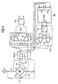
- FIG. 1 is a block circuit diagram of a first exemplary embodiment of the amplifier circuit according to the invention.
- FIG. 2 is a block circuit diagram of a more detailed exemplary embodiment according to FIG. 1 in the first clock phase;
- FIG. 3 is a block circuit diagram of the circuit according to FIG. 2 in the second clock phase
- FIG. 4 is a block circuit diagram of an exemplary embodiment of the present invention with the error signals coupled out at the amplifier input;
- FIG. 5 is a block circuit diagram of an exemplary embodiment of the invention with an additional demodulator in the error signal branch;
- FIG. 6 is an equivalent circuit of the Hall sensor in FIG. 2;
- FIG. 7 is an equivalent circuit of the Hall sensor in FIG. 3.
- FIG. 8 is a circuit diagram of an exemplary embodiment of the additional demodulator shown in FIG. 5 .
- the circuit has an amplifier OP 1 wit inputs connected to a Hall sensor HS.
- the Hall sensor HS is connected via a modulator MOD 1 to the amplifier OP 1 and also a current source Q 1 for supplying an excitation current.
- the Hall element HS is penetrated by a magnetic field B.
- the Hall element HS has four. terminals K 1 to K 4 , of which in each case two opposite terminals are connected to the excitation current source Q 1 and two others to the inputs of the amplifier OP 1 .
- a first demodulator DEM 1 which has means of reversing the polarity of the signal lines executed in the differential path technique for carrying the measured signals, is connected downstream of the operational amplifier OP 1 .
- the first modulator MOD 1 and the first demodulator DEM 1 are connected to a clock generator TG in order to supply a chopping cycle frequency.
- a second low-pass filter TP 2 is connected downstream of the first demodulator DEM 1 .
- the second low-pass filter TP 2 is used to filter peaks caused by changeover operations.
- an error signal demodulator FD 1 which has a first low-pass filter TP 1 with an amplifier V 1 connected downstream, is connected to the output side of the amplifier OP 1 .
- the amplifier output from the amplifier V 1 is connected to the inverting input of the operational amplifier OP 1 , forming a negative feedback loop.
- the amplifier V 1 is a transconductance amplifier or a voltage amplifier with a resistor on the output side.
- the modulator MOD 1 is used to implement a periodic 90° changeover of pairs of terminals of the Hall sensor HS at the chopping cycle rate of the clock generator TG.
- the measured signals produced in this way which have a useful signal component and an offset component, are supplied to the operational amplifier OP 1 in the differential path technique and are amplified there.
- the offset component of the measured signals is coupled out from the measured signals by the first low-pass filter TP 1 and, amplified, is fed back to the operational amplifier input. In this way, even after a few clock cycles, the offset component of the measured signals is reduced sharply. Consequently, the drive range of the operational amplifier OP 1 can be reduced considerably as compared with conventional amplifiers operated in chopped mode.
- the subsequent filter complexity can be kept low, and delay times and noise can be reduced significantly.
- first low-pass filter TP 1 instead of the first low-pass filter TP 1 , integration elements, summing junctions or averagers can be provided.
- FIG. 2 shows a development of the amplifier circuit according to FIG. 1 in the first clock phase, while the switching states of the circuit according to FIG. 2 during the second clock phase are illustrated in FIG. 3 .
- an excitation current I 1 is conducted through the Hall sensor via the terminals K 1 and K 3 .
- the Hall voltage UH 1 during the first clock phase (CLK 1 ) can be tapped off at terminals K 2 and K 4 .
- the operational amplifier OP 2 according to FIG. 2 is designed as an instrumentation amplifier. That means, it has two differential amplifiers D 1 and D 1 ′, whose noninverting inputs are each connected to the outputs of the modulator MOD 2 .
- the inverting inputs of the differential amplifiers D 1 , D 1 ′ are connected to each other via a first resistor R 1 .
- Feed back resistors R 2 , R 2 ′ in each case connect the differential amplifier output to the inverting input of the differential amplifiers D 1 , D 1 ′.
- the error signal demodulator FD 2 connected to the output of the operational amplifier OP 2 again has a low-pass filter TP 1 with transconductance amplifiers V 2 , V 2 ′ connected downstream, whose outputs are each connected to the inverting inputs of the differential amplifiers D 1 , D 1 ′.
- the transconductance amplifiers V 2 , V 2 ′ can be voltage amplifiers with a resistor on the output side or, instead of the two transconductance amplifiers V 2 , V 2 ′, one transconductance amplifier (OTA) with two inputs and two outputs (differential in, differential out) can be provided.
- OTA transconductance amplifier
- FIG. 4 shows a further exemplary embodiment of the present invention, wherein the offset components and the error signals, respectively, are coupled out not downstream but upstream of the operational amplifier OP 2 .
- the error signal demodulator FD 2 has a difference-forming module DB connected upstream, which forms the difference of the measured signal differential voltage U 1 and the differential voltage across the resistor R 1 in the operational amplifier OP 2 .
- the useful signal is present as a DC signal.
- the circuit configuration according to FIG. 4 is shown during the first clock phase.
- the second clock phase can be derived in a simple way by analogy with FIG. 3 .
- the excitation current supply and Hall voltage tap are rotated in the same direction.
- four switches are provided, which are connected to the nodes K 1 to K 4 .
- the difference former DB in each case forms the difference between the differential voltages U 1 , U 2 both in the first and in the second clock phase.
- the first low-pass filter TP 1 connected downstream sums or integrates the difference U 1 ⁇ U 2 between the differential voltages U 1 , U 2 in each case in the first and the second clock phase.
- the demodulator DEM 2 can be omitted.
- the differential amplifiers D 1 , D 1 ′ according to FIG. 4 are designed as operational amplifiers, while the amplifiers V 2 , V 2 ′ of the error signal demodulator FD 2 are designed as transconductance amplifiers.
- voltage amplifiers with a resistance on the output side can be provided instead of the transconductance amplifiers.
- the chopping clock which can be supplied to the modulator MOD 2 can additionally be supplied to the first low-pass filter TP 1 .
- FIG. 5 shows a development of the exemplary embodiment according to FIG. 1 .
- an additional demodulator DEM 3 is arranged between the output of the amplifier OP 1 and the first low-pass filter TP 1 .
- the additional demodulator DEM 3 is connected to the clock generator TG, which also drives the modulator MOD 1 and the demodulator DEM 1 arranged in the useful signal path.
- the additional demodulator DEM 3 in this case forms the sum or the average in the correct phase over two successive clock phases.
- the feedback supply of the signals that can be tapped off on the output side of the error signal demodulator can be provided on the input side of the Hall element.
- additional switches driven in correct phase by the clock generator can be provided.
- the first low-pass filter TP 1 averagers, summers or an integrator can be provided.
- FIG. 6 shows an equivalent circuit of the Hall sensor HS from FIG. 2 during the first clock phase.
- resistors R are arranged between the four terminals K 1 to K 4 of the Hall sensor, of which the resistor between K 1 and K 4 has a deviation ⁇ R from the remaining resistance values between the adjacent terminals K 1 to K 4 .
- the deviation ⁇ R from the resistance value R of the resistor between the first and fourth terminals K 1 , K 4 represents the cause for the direction-dependent offset voltage of the Hall element.
- the excitation current I 1 is impressed into the Hall element HS via a first pair of terminals K 1 , K 3 .
- the first measured signal UH 1 can be tapped off via the second pair of terminals K 2 , K 4 when the Hall element is penetrated by a magnetic field B.
- FIG. 7 shows the equivalent circuit according to FIG. 6 during the second clock phase and is accordingly an equivalent circuit for the Hall sensor HS according to FIG. 3 .
- the connections for excitation current and second measured signal are rotated through 90° as compared with FIG. 6 .
- the second measured signal UH 2 can be tapped off via the first pair of terminals K 1 , K 3 when the excitation current I 1 is supplied via the second pair of terminals K 2 , K 4 of the Hall element penetrated by a magnetic field B.
- the first and the second measured signal differ in that the first measured signal UH 1 is formed from the sum of useful component and offset component, while the second measured signal UH 2 , present during the second clock phase, is formed from the difference between useful component and offset component.
- FIG. 8 shows a block circuit diagram wherein a pole reversal switch is provided.
- the circuit according to FIG. 8 can replace the demodulator DEM 3 in FIG. 5 .
- the circuit according to FIG. 8 is implemented using the single-ended technique. However, the principle described can also be implemented in the differential path technique.
- the amplifier (not shown here) for amplifying-the measured signals has a first switch S 1 connected downstream which, during the first cycle phase, connects the first measured signal UH 1 to a first capacitor C 1 and, during the second cycle phase, connects the second, negative measured signal UH 2 to a second capacitor C 2 .
- the first switch S 1 is connected to a clock generator TG for supplying a chopping clock.
- the first and second capacitors C 1 , C 2 are in each case connected to ground.
- a pole reversal switch VS for changing the polarity of the lines for the first and second measured signals UH 1 , UH 2 , and also amplifiers V 3 , V 4 and resistors R 3 , R 4 , whose connections on the output side are connected to each other, are connected downstream of the first and second capacitors C 1 , C 2 .
- the pole reversal switch VS is driven by the chopping clock, just like the first switch S 1 .
- the demodulator is used for error modulation by feeding back an error signal, but not for demodulation in the signal branch itself. Filters which are offset-free and consequently do not cause any additional errors caused by changes in the useful signal can be arranged in the signal branch.
- the invention can also be applied in what is known as the spinning Hall principle, wherein it is not just two pairs of terminals and accordingly two clock phases which are provided, but wherein the Hall element has N pairs of terminals and accordingly N clock phases.
Landscapes
- Engineering & Computer Science (AREA)
- Power Engineering (AREA)
- Physics & Mathematics (AREA)
- Condensed Matter Physics & Semiconductors (AREA)
- General Physics & Mathematics (AREA)
- Measuring Magnetic Variables (AREA)
- Amplifiers (AREA)
- Hall/Mr Elements (AREA)
Abstract
An amplifier circuit with offset compensation is particularly suited for a Hall element. In addition to the useful signal demodulation that is normally present and connected downstream of an amplifier, an error signal demodulator provides an error signal demodulation. The measured signals that are tapped off at the Hall sensor are coupled out at the input or output of the amplifier, and a demodulated error signal is fed back to the input of the amplifier. This makes it possible to reduce the drive range of the amplifier. The amplifier circuit is suitable in particular for Hall sensors that are operated in chopped mode.
Description
This application is a continuation of copending international application PCT/DE01/02438, filed Jun. 29, 2001, which designated the United States and which was not published in English.
The invention relates to an amplifier circuit with offset compensation, in particular for magnetic field sensors operated in chopped mode.
Sensors, for example magnetic field sensors, usually need an offset error correction in order to operate precisely. In the case of integrated Hall elements operating as magnetic field sensors, an offset error can arise, for example, because of fabrication-induced bending of the silicon platelet (mechanical stress) or as a result of lithographic inaccuracies during the production process. Further offset errors can be caused by the external wiring of the Hall sensor, for example as a result of offset voltages in amplifiers connected downstream of the Hall sensor. U.S. Pat. No. 5,621,319 to Bilotti et al. specifies a method for compensating for the offset voltage normally occurring in Hall sensors. There, two pairs of terminals that are arranged orthogonally with respect to each other are provided on the Hall sensor. In each case one pair of terminals is fed with the excitation current and the Hall voltage is available on the other pair of terminals. A change between the pairs of terminals is made at the chopping cycle rate. In this way, the alternating voltage error signal is reduced.
A development of that chopped-Hall principle to a Hall sensor having N pairs of connecting terminals, which are interchanged cyclically—it is thereby possible for the Hall voltage to be picked off on one pair of terminals in each case which is arranged orthogonally with respect to the pair of terminals of the excitation current—is specified in the document “Spinning-Current Method for Offset Reduction in Silicon Hall Plates” by Peter Jahn Adriaan Munter, Delft University Press, 1992, page 12.
The common factor in the above-described offset compensation methods for magnetic field sensors is that in the amplifier connected downstream of the magnetic field sensor, both the useful signal and the chopped error signal have to be amplified considerably for further processing or demodulation. This requires high driveability of the amplifier stages, which stands in the way of the requirement for a lower and lower internal operating voltage. In order to suppress the alternating voltage error signal adequately, comprehensive circuit measures are required.
Furthermore, the above-described sampling of the useful signal then leads to an additional error when the useful signal changes. In the case of time-critical applications, this error signal additionally has to be filtered out of the useful signal.
Further disadvantages of the above-described offset compensation method reside firstly in the fact that, because of the offset-afflicted buffer amplifiers which are used in the sample-and-hold circuits, additional, undesired offsets are produced and, secondly, further offsets arise as the result of the use of summing resistors which have mismatches. Although these offsets are reduced in accordance with the chopped-Hall principle, they are not eliminated completely.
It is accordingly an object of the invention to provide an amplifier circuit with offset compensation which overcomes the above-mentioned disadvantages of the heretofore-known devices and methods of this general type and which is suitable for Hall sensors operated in chopped mode, requires a low drive range and needs little expenditure on filtering in order to suppress alternating voltage error signals.
With the foregoing and other objects in view there is provided, in accordance with the invention, an amplifier circuit with offset compensation, comprising:
a signal source for outputting a first measured signal in a first clock phase and a second measured signal in a second clock phase, each of the first and second measured signals having a useful component and, possibly, an offset component;
an amplifier having an input side connected to said signal source for receiving the measured signals and having an output side for carrying amplified measured signals;
an error signal demodulator connected to one of said input side and said output side of said amplifier for receiving the measured signals; and
said error signal demodulator having an output connected to an input at said input side of said amplifier for supplying the offset component in antiphase.
In other words, the objects of the invention are achieved by an amplifier circuit with offset compensation as outlined. The amplifier circuit includes a signal source, on which a first measured signal can be tapped off in a first clock phase and a second measured signal can be tapped off in a second clock phase, the measured signals in each case having a useful component and possibly having an offset component. The circuit furthermore has an amplifier which, on the input side, is connected to the signal source for the supply of the measured signals and on whose output the amplified measured signals are provided. An error signal demodulator is connected to the input or output of the amplifier in order to supply the measured signals, and the demodulator has an output that is connected to an input of the amplifier in antiphase in order to supply the offset component.
According to the principle of the present invention, the offset component of the first and second measured signals is in each case coupled out of the measured signals by an error signal demodulator, the error signal is demodulated and then the demodulated error signal is fed back to the input of the amplifier. In this way, the error signal or the offset component of the measured signals is already eliminated at the amplifier input, so that the drive range of the amplifier only has to be matched to the useful component of the measured signals. Consequently, the drive range of the amplifier can be reduced considerably. The result is, therefore, a saving of chip area with higher accuracy of the circuit. In addition, the result overall is a lower delay time, caused only by the amplifier circuit. Furthermore, error signals which are caused by changing the useful signal are avoided as a result of avoiding sampling processing in the main signal branch.
After the amplifier circuit has been switched on, first of all both the useful component and the offset component of the measured signals and also amplifier offset signals are amplified in the amplifier. Even after a few clock cycles, the error signal antiphase coupling leads to the offset components being considerably reduced without falsifying the useful components.
In the antiphase coupling of the error signal, an integrator can be provided, by which means offsets are virtually completely eliminated.
Further advantages consist in the lower expenditure on filtering of the measuring signals, since the output ripple in measured signal ramps is reduced sharply. Since, for the further processing of the measured signals to be carried out on the output side of the amplifier, in particular of the useful component of the measured signals, a lower analog bandwidth is required, the noise characteristics of the amplifier circuit are improved. Finally, the aliasing errors are reduced in the amplifier circuit described, since no sampling-signal processing is carried out in the main signal path.
The signal source can be a magnetic field sensor.
In a preferred embodiment of the present invention, the measured signals are carried by using the differential path technique. In this way, common mode interference is suppressed.
In a further, advantageous embodiment of the present invention, a modulator which has means for reversing the polarity of the measured signal lines is arranged between magnetic field sensor and amplifier, and a demodulator which has means of reversing the polarity of the measured signal lines is arranged at the amplifier output. The means of reversing the polarity of the measured signal lines in the modulator and demodulator can be driven at a common chopping cycle rate.
If the signal source is a Hall sensor operated in chopped mode, the amplifier circuit can have 90° changeover switches for excitation current connections and signal outputs for the measured signals, which can be arranged in the modulator.
In accordance with a further, advantageous embodiment of the present invention, the error signal demodulator has a first low-pass filter and an amplifier connected downstream with a resistance on the output side. The amplifier can be a transconductance amplifier (OTA, operational transconductance amplifier). Instead of the low-pass filter, a summing junction or an integrator can be provided, in each case with an amplifier connected downstream.
In accordance with another feature of the invention, the amplifier can have a second low-pass filter connected downstream, which can be implemented with RC elements constructed in analog fashion. This makes it possible, in accordance with the principle of dynamic element interchange, to interchange the tolerance-afflicted resistors periodically, in order to compensate for their fabrication-induced tolerances.
The magnetic field sensor can have a Hall element. If the signal source is not a Hall element, the measured signals do not necessarily have to have an offset component. In this case, nevertheless, compensation is carried out, specifically the compensation of the offset of the (chopper) amplifier itself.
For chopping operation, the Hall element can have two orthogonal pairs of terminals, wherein in each case the excitation current is supplied to one pair of terminals and the Hall voltage, that is to say the first or second measured signal, can be tapped off at the other pair of terminals.
The error signal can be coupled out on the input side or output side of the amplifier.
The first low-pass filter in the error signal demodulator can of course be replaced by summing the signal voltages over the two clock phases or by averaging the voltages over the two clock phases. The first low-pass filter in the error signal demodulator can be replaced by an integrator.
Other features which are considered as characteristic for the invention are set forth in the appended claims.
Although the invention is illustrated and described herein as embodied in a amplifier circuit with offset compensation, it is nevertheless not intended to be limited to the details shown, since various modifications and structural changes may be made therein without departing from the spirit of the invention and within the scope and range of equivalents of the claims.
The construction and method of operation of the invention, however, together with additional objects and advantages thereof will be best understood from the following description of specific embodiments when read in connection with the accompanying drawings.
FIG. 1 is a block circuit diagram of a first exemplary embodiment of the amplifier circuit according to the invention;
FIG. 2 is a block circuit diagram of a more detailed exemplary embodiment according to FIG. 1 in the first clock phase;
FIG. 3 is a block circuit diagram of the circuit according to FIG. 2 in the second clock phase;
FIG. 4 is a block circuit diagram of an exemplary embodiment of the present invention with the error signals coupled out at the amplifier input;
FIG. 5 is a block circuit diagram of an exemplary embodiment of the invention with an additional demodulator in the error signal branch;
FIG. 6 is an equivalent circuit of the Hall sensor in FIG. 2;
FIG. 7 is an equivalent circuit of the Hall sensor in FIG. 3; and
FIG. 8 is a circuit diagram of an exemplary embodiment of the additional demodulator shown in FIG. 5.
Referring now to the figures of the drawing in detail and first, particularly, to FIG. 1 thereof, there is illustrated the present principle of an amplifier circuit with offset compensation. The circuit has an amplifier OP1 wit inputs connected to a Hall sensor HS. The Hall sensor HS is connected via a modulator MOD1 to the amplifier OP1 and also a current source Q1 for supplying an excitation current. The Hall element HS is penetrated by a magnetic field B. The Hall element HS has four. terminals K1 to K4, of which in each case two opposite terminals are connected to the excitation current source Q1 and two others to the inputs of the amplifier OP1. In the useful signal path, a first demodulator DEM1, which has means of reversing the polarity of the signal lines executed in the differential path technique for carrying the measured signals, is connected downstream of the operational amplifier OP1. The first modulator MOD1 and the first demodulator DEM1 are connected to a clock generator TG in order to supply a chopping cycle frequency. A second low-pass filter TP2 is connected downstream of the first demodulator DEM1. The second low-pass filter TP2 is used to filter peaks caused by changeover operations. Furthermore, an error signal demodulator FD1, which has a first low-pass filter TP1 with an amplifier V1 connected downstream, is connected to the output side of the amplifier OP1. The amplifier output from the amplifier V1 is connected to the inverting input of the operational amplifier OP1, forming a negative feedback loop. The amplifier V1 is a transconductance amplifier or a voltage amplifier with a resistor on the output side.
The modulator MOD1 is used to implement a periodic 90° changeover of pairs of terminals of the Hall sensor HS at the chopping cycle rate of the clock generator TG. The measured signals produced in this way, which have a useful signal component and an offset component, are supplied to the operational amplifier OP1 in the differential path technique and are amplified there. The offset component of the measured signals is coupled out from the measured signals by the first low-pass filter TP1 and, amplified, is fed back to the operational amplifier input. In this way, even after a few clock cycles, the offset component of the measured signals is reduced sharply. Consequently, the drive range of the operational amplifier OP1 can be reduced considerably as compared with conventional amplifiers operated in chopped mode. The subsequent filter complexity can be kept low, and delay times and noise can be reduced significantly.
Instead of the first low-pass filter TP1, integration elements, summing junctions or averagers can be provided.
FIG. 2 shows a development of the amplifier circuit according to FIG. 1 in the first clock phase, while the switching states of the circuit according to FIG. 2 during the second clock phase are illustrated in FIG. 3.
According to FIG. 2, an excitation current I1 is conducted through the Hall sensor via the terminals K1 and K3. The Hall voltage UH1 during the first clock phase (CLK1) can be tapped off at terminals K2 and K4. During the first clock phase, it is ensured that the measured signals are led through the modulator MOD2 and demodulator DEM2 without any polarity reversal. The operational amplifier OP2 according to FIG. 2 is designed as an instrumentation amplifier. That means, it has two differential amplifiers D1 and D1′, whose noninverting inputs are each connected to the outputs of the modulator MOD2. The inverting inputs of the differential amplifiers D1, D1′ are connected to each other via a first resistor R1. Feed back resistors R2, R2′ in each case connect the differential amplifier output to the inverting input of the differential amplifiers D1, D1′. The error signal demodulator FD2 connected to the output of the operational amplifier OP2 again has a low-pass filter TP1 with transconductance amplifiers V2, V2′ connected downstream, whose outputs are each connected to the inverting inputs of the differential amplifiers D1, D1′. In an alternative embodiment, the transconductance amplifiers V2, V2′ can be voltage amplifiers with a resistor on the output side or, instead of the two transconductance amplifiers V2, V2′, one transconductance amplifier (OTA) with two inputs and two outputs (differential in, differential out) can be provided.
In FIG. 3, during the second clock phase (CLK2), the switches in the modulator MOD2 and demodulator DEM2 are switched in such a way that the measured signals carried in the differential path technique in each case have their polarity reversed. In addition, the excitation current supply and Hall voltage tap are rotated through 90° on the Hall sensor HS with respect to FIG. 2. In this case, the 90° rotation of the excitation current supply and of the Hall voltage tap are carried out in the opposite direction of rotation.
FIG. 4 shows a further exemplary embodiment of the present invention, wherein the offset components and the error signals, respectively, are coupled out not downstream but upstream of the operational amplifier OP2. In contrast with the exemplary embodiment according to FIG. 2, in this case the error signal demodulator FD2 has a difference-forming module DB connected upstream, which forms the difference of the measured signal differential voltage U1 and the differential voltage across the resistor R1 in the operational amplifier OP2. The useful signal is present as a DC signal.
The circuit configuration according to FIG. 4 is shown during the first clock phase. The second clock phase can be derived in a simple way by analogy with FIG. 3. In this case, the excitation current supply and Hall voltage tap are rotated in the same direction. In order to change over the excitation current supply and Hall voltage tap, four switches are provided, which are connected to the nodes K1 to K4.
The difference former DB in each case forms the difference between the differential voltages U1, U2 both in the first and in the second clock phase. The first low-pass filter TP1 connected downstream sums or integrates the difference U1−U2 between the differential voltages U1, U2 in each case in the first and the second clock phase.
In the circuit according to FIG. 4, the demodulator DEM2 can be omitted. The differential amplifiers D1, D1′ according to FIG. 4 are designed as operational amplifiers, while the amplifiers V2, V2′ of the error signal demodulator FD2 are designed as transconductance amplifiers. In an alternative embodiment, instead of the transconductance amplifiers, voltage amplifiers with a resistance on the output side can be provided.
The chopping clock which can be supplied to the modulator MOD2 can additionally be supplied to the first low-pass filter TP1.
FIG. 5 shows a development of the exemplary embodiment according to FIG. 1. In this case, an additional demodulator DEM3 is arranged between the output of the amplifier OP1 and the first low-pass filter TP1. In order to supply a clock signal, the additional demodulator DEM3 is connected to the clock generator TG, which also drives the modulator MOD1 and the demodulator DEM1 arranged in the useful signal path. The additional demodulator DEM3 in this case forms the sum or the average in the correct phase over two successive clock phases.
In an alternative embodiment to FIG. 5, the feedback supply of the signals that can be tapped off on the output side of the error signal demodulator can be provided on the input side of the Hall element. For this purpose, additional switches driven in correct phase by the clock generator can be provided. Instead of the first low-pass filter TP1, averagers, summers or an integrator can be provided.
FIG. 6 shows an equivalent circuit of the Hall sensor HS from FIG. 2 during the first clock phase. According to the equivalent circuit of FIG. 6, in each case resistors R are arranged between the four terminals K1 to K4 of the Hall sensor, of which the resistor between K1 and K4 has a deviation ΔR from the remaining resistance values between the adjacent terminals K1 to K4. The deviation ΔR from the resistance value R of the resistor between the first and fourth terminals K1, K4 represents the cause for the direction-dependent offset voltage of the Hall element. The excitation current I1 is impressed into the Hall element HS via a first pair of terminals K1, K3. The first measured signal UH1 can be tapped off via the second pair of terminals K2, K4 when the Hall element is penetrated by a magnetic field B.
FIG. 7 shows the equivalent circuit according to FIG. 6 during the second clock phase and is accordingly an equivalent circuit for the Hall sensor HS according to FIG. 3. In this case, the connections for excitation current and second measured signal are rotated through 90° as compared with FIG. 6. Accordingly, the second measured signal UH2 can be tapped off via the first pair of terminals K1, K3 when the excitation current I1 is supplied via the second pair of terminals K2, K4 of the Hall element penetrated by a magnetic field B.
According to the equivalent circuits of FIGS. 6 and 7, the first and the second measured signal differ in that the first measured signal UH1 is formed from the sum of useful component and offset component, while the second measured signal UH2, present during the second clock phase, is formed from the difference between useful component and offset component.
FIG. 8 shows a block circuit diagram wherein a pole reversal switch is provided. The circuit according to FIG. 8 can replace the demodulator DEM3 in FIG. 5. Here, it should be noted that the circuit according to FIG. 8 is implemented using the single-ended technique. However, the principle described can also be implemented in the differential path technique.
In the circuit according to FIG. 8, the amplifier (not shown here) for amplifying-the measured signals has a first switch S1 connected downstream which, during the first cycle phase, connects the first measured signal UH1 to a first capacitor C1 and, during the second cycle phase, connects the second, negative measured signal UH2 to a second capacitor C2. To this end, the first switch S1 is connected to a clock generator TG for supplying a chopping clock. The first and second capacitors C1, C2 are in each case connected to ground. Furthermore, a pole reversal switch VS for changing the polarity of the lines for the first and second measured signals UH1, UH2, and also amplifiers V3, V4 and resistors R3, R4, whose connections on the output side are connected to each other, are connected downstream of the first and second capacitors C1, C2. The pole reversal switch VS is driven by the chopping clock, just like the first switch S1. The circuit according to FIG. 5 has the advantage that unavoidable, fabrication-induced deviations of the resistance values of the resistors R3, R4 from each other can be compensated for by the above-described, correct-phase reversal of polarity of the lines carrying the first and second measured signals UH1, UH2, respectively. Formed at the output, therefore, is the average of the offset signal, from which the alternating voltage useful signal has been removed.
The principle described is designated the dynamic element interchange and avoids offsets caused by mismatches. In the demodulator configuration according to FIG. 8, the demodulator is used for error modulation by feeding back an error signal, but not for demodulation in the signal branch itself. Filters which are offset-free and consequently do not cause any additional errors caused by changes in the useful signal can be arranged in the signal branch.
The invention can also be applied in what is known as the spinning Hall principle, wherein it is not just two pairs of terminals and accordingly two clock phases which are provided, but wherein the Hall element has N pairs of terminals and accordingly N clock phases.
Even in a Hall element having only two pairs of terminals, four clock phases can be formed by the excitation current being fed into the Hall element in 90° steps and by it being possible to tap off the measured signal in each case orthogonally with respect to the excitation current.
Claims (11)
1. An amplifier circuit with offset compensation, comprising:
a signal source for outputting a first measured signal in a first clock phase and a second measured signal in a second clock phase, each of the first and second measured signals having a useful component and, possibly, an offset component;
an amplifier having an input side connected to said signal source for receiving the measured signals and having an output side for carrying amplified measured signals;
an error signal demodulator connected to one of said input side and said output side of said amplifier for receiving the measured signals; and
said error signal demodulator having an output connected to an input at said input side of said amplifier for supplying the offset component in antiphase.
2. The amplifier circuit according to claim 1 , wherein said signal source is a magnetic field sensor.
3. The amplifier circuit according to claim 1 , wherein the measured signals are carried in differential path technique.
4. The amplifier circuit according to claim 3 , which comprises a modulator capable of reversing a polarity of the measured signal lines connected between said magnetic field sensor and said amplifier, and a demodulator connected at said output side of said amplifier adapted to reverse the polarity of the measured signal lines.
5. The amplifier circuit according to claim 4 , wherein said error signal demodulator includes a low-pass filter and at least one amplifier connected to an output of said low-pass filter.
6. The amplifier circuit according to claim 1 , wherein said error signal demodulator includes a first low-pass filter, and a second low-pass filter is connected to the output side of said amplifier.
7. The amplifier circuit according to claim 6 , wherein said second low-pass filter is an analog RC element.
8. The amplifier circuit according to claim 7 , wherein said second low-pass filter is provided in said demodulator, and said demodulator comprises means for reversing polarity and resistors connected downstream of said means for reversing polarity.
9. The amplifier circuit according to claim 4 , wherein said second low-pass filter is provided in said demodulator, and said demodulator comprises means for reversing polarity and resistors connected downstream of said means for reversing polarity.
10. The amplifier circuit according to claim 2 , wherein the magnetic field sensor has a Hall element.
11. The amplifier circuit according to claim 10 , wherein said Hall element has two mutually orthogonal pairs of terminals, said pairs of terminals including a first pair of terminals receiving an excitation current in the first clock phase and a second pair of terminals carrying the first measured signal in the first clock phase, and wherein said second pair of terminals receives the excitation current in the second clock phase and said first pair of terminals carries the second measured signal in the second clock phase.
Applications Claiming Priority (4)
| Application Number | Priority Date | Filing Date | Title |
|---|---|---|---|
| DE10032530 | 2000-07-05 | ||
| DE10032530A DE10032530C2 (en) | 2000-07-05 | 2000-07-05 | Amplifier circuit with offset compensation |
| DE10032530.0 | 2000-07-05 | ||
| PCT/DE2001/002438 WO2002003087A1 (en) | 2000-07-05 | 2001-06-29 | Amplifier circuit with offset compensation |
Related Parent Applications (1)
| Application Number | Title | Priority Date | Filing Date |
|---|---|---|---|
| PCT/DE2001/002438 Continuation WO2002003087A1 (en) | 2000-07-05 | 2001-06-29 | Amplifier circuit with offset compensation |
Publications (2)
| Publication Number | Publication Date |
|---|---|
| US20030102909A1 US20030102909A1 (en) | 2003-06-05 |
| US6674322B2 true US6674322B2 (en) | 2004-01-06 |
Family
ID=7647779
Family Applications (1)
| Application Number | Title | Priority Date | Filing Date |
|---|---|---|---|
| US10/337,194 Expired - Lifetime US6674322B2 (en) | 2000-07-05 | 2003-01-06 | Amplifier circuit with offset compensation |
Country Status (5)
| Country | Link |
|---|---|
| US (1) | US6674322B2 (en) |
| EP (1) | EP1297349B1 (en) |
| KR (1) | KR100508619B1 (en) |
| DE (2) | DE10032530C2 (en) |
| WO (1) | WO2002003087A1 (en) |
Cited By (40)
| Publication number | Priority date | Publication date | Assignee | Title |
|---|---|---|---|---|
| US20030155912A1 (en) * | 2002-02-04 | 2003-08-21 | Mario Motz | Method and apparatus for the compensation of dynamic error signals of a chopped hall sensor |
| US20030225539A1 (en) * | 2002-05-28 | 2003-12-04 | Mario Motz | Circuit configuration for processing a signal of a sensor and method of using the circuit configuration |
| US20050001613A1 (en) * | 2003-03-26 | 2005-01-06 | Lothar Blossfeld | Offset-reduced hall sensor |
| US20060192550A1 (en) * | 2005-02-25 | 2006-08-31 | Sandquist David A | Current sensor with magnetic toroid single frequency detection scheme |
| US20060226898A1 (en) * | 2005-03-29 | 2006-10-12 | Linear Technology Corporation | Offset correction circuit for voltage-controlled current source |
| US20070030060A1 (en) * | 2005-08-03 | 2007-02-08 | Swanson Leland S | Apparatus and method for effecting signal chopping in an amplifier device |
| US7197292B1 (en) | 2004-09-01 | 2007-03-27 | National Semiconductor Corporation | Chopper stabilized analog multiplier |
| US20070146065A1 (en) * | 2005-08-08 | 2007-06-28 | Hirokazu Yoshizawa | Chopper amplifier circuit and semiconductor device |
| US20070270116A1 (en) * | 2004-09-01 | 2007-11-22 | Kouwenhoven Michael Hendrikus | Extended range RMS-DC converter |
| US20080180278A1 (en) * | 2007-01-31 | 2008-07-31 | Medtronic, Inc. | Chopper-stabilized instrumentation amplifier for wireless telemetry |
| US20080197834A1 (en) * | 2007-02-19 | 2008-08-21 | Kabushiki Kaisha Toshiba | Signal detecting circuit |
| US20080269841A1 (en) * | 2007-04-30 | 2008-10-30 | Medtronic, Inc. | Chopper mixer telemetry circuit |
| US20090009164A1 (en) * | 2007-06-14 | 2009-01-08 | Oki Electric Industry Co., Ltd. | Magneto-sensitive integrated circuit |
| US20090082691A1 (en) * | 2007-09-26 | 2009-03-26 | Medtronic, Inc. | Frequency selective monitoring of physiological signals |
| US7518443B2 (en) | 2004-09-10 | 2009-04-14 | Quantum Applied Science & Research, Inc. | Amplifier circuit and method for reducing voltage and current noise |
| US20090315549A1 (en) * | 2006-07-14 | 2009-12-24 | Fraunhofer-Gesellschaft Zur Forderung Der Angewandten Forschung E.V. | Method for processing sensor signals subject to an offset and sensor arrangement designed to carry out the method |
| US20100033240A1 (en) * | 2007-01-31 | 2010-02-11 | Medtronic, Inc. | Chopper-stabilized instrumentation amplifier for impedance measurement |
| US7710298B2 (en) | 2008-07-01 | 2010-05-04 | Infineon Technologies Ag | Integrated circuit with auto-zeroing comparator stages that provide a continuous-time signal |
| US20100114223A1 (en) * | 2008-10-31 | 2010-05-06 | Wahlstrand John D | Determining intercardiac impedance |
| US20100327887A1 (en) * | 2007-01-31 | 2010-12-30 | Medtronic, Inc. | Chopper-stabilized instrumentation amplifier for impedance measurement |
| US20110068861A1 (en) * | 2007-01-31 | 2011-03-24 | Medtronic, Inc. | Chopper-stabilized instrumentation amplifier |
| US20110215955A1 (en) * | 2010-03-04 | 2011-09-08 | Infineon Technologies Ag | System including feedback circuit with digital chopping circuit |
| US20110260723A1 (en) * | 2010-04-23 | 2011-10-27 | Samsung Electro-Mechanics Co., Ltd. | Hall device and magnetic sensor circuit |
| US8422970B1 (en) | 2008-08-28 | 2013-04-16 | National Semiconductor Corporation | RMS power detection with signal-independent dynamics and related apparatus, system, and method |
| WO2013111521A1 (en) | 2012-01-25 | 2013-08-01 | 旭化成エレクトロニクス株式会社 | Hall electromotive force signal detection circuit and current sensor thereof |
| US20140118048A1 (en) * | 2012-10-30 | 2014-05-01 | Yamaha Corporation | Offset Cancel Circuit |
| US8829988B2 (en) * | 2012-09-14 | 2014-09-09 | Infineon Technologies Ag | Chopped circuit with AC and DC ripple error feedback loops |
| US9063198B2 (en) | 2012-02-29 | 2015-06-23 | Asahi Kasei Microdevices Corporation | Current sensor having self-diagnosis function and signal processing circuit |
| US9248288B2 (en) | 2007-09-26 | 2016-02-02 | Medtronic, Inc. | Patient directed therapy control |
| US9577619B2 (en) | 2014-02-05 | 2017-02-21 | Samsung Electronics Co., Ltd. | Buffer circuit having amplifier offset compensation and source driving circuit including the same |
| US9614481B2 (en) * | 2015-03-31 | 2017-04-04 | Analog Devices, Inc. | Apparatus and methods for chopping ripple reduction in amplifiers |
| US9685967B1 (en) | 2016-09-08 | 2017-06-20 | Infineon Technologies Ag | Chopper stabilized sigma delta ADC |
| US9706957B2 (en) | 2008-01-25 | 2017-07-18 | Medtronic, Inc. | Sleep stage detection |
| US20170234910A1 (en) * | 2014-09-26 | 2017-08-17 | Asahi Kasei Microdevices Corporation | Hall electromotive force signal detection circuit and current sensor |
| US9770204B2 (en) | 2009-11-11 | 2017-09-26 | Medtronic, Inc. | Deep brain stimulation for sleep and movement disorders |
| US9924904B2 (en) | 2014-09-02 | 2018-03-27 | Medtronic, Inc. | Power-efficient chopper amplifier |
| WO2018109351A1 (en) | 2016-12-13 | 2018-06-21 | Seb S.A. | Method for dynamic compensation for the offset error of an acquisition system comprising a current sensor |
| US11047933B2 (en) * | 2019-04-02 | 2021-06-29 | Allegro Microsystems, Llc | Fast response magnetic field sensors and associated methods for removing undesirable spectral components |
| US11406830B2 (en) | 2016-09-02 | 2022-08-09 | Medtronic, Inc. | Hall sensor circuit for magnetic field detection in implantable medical device |
| US12334185B2 (en) | 2023-03-03 | 2025-06-17 | Samsung Electronics Co., Ltd. | Memory systems and devices that support methods for calibrating input offsets therein |
Families Citing this family (109)
| Publication number | Priority date | Publication date | Assignee | Title |
|---|---|---|---|---|
| DE10160794B4 (en) * | 2001-12-11 | 2006-07-27 | Parker Hannifin Gmbh | Signal processing device for a pressure switch od. Like. |
| DE102004021863A1 (en) * | 2004-05-04 | 2005-12-01 | Infineon Technologies Ag | Sensor element for providing a sensor signal and method for operating a sensor element |
| DE102004022572B4 (en) | 2004-05-07 | 2012-02-16 | Infineon Technologies Ag | integrator circuit |
| KR101167880B1 (en) | 2005-08-08 | 2012-07-23 | 각코우호진 지코우지가쿠엔 | Chopper amplifier circuit and semiconductor device |
| US7425821B2 (en) | 2006-10-19 | 2008-09-16 | Allegro Microsystems, Inc. | Chopped Hall effect sensor |
| US7675245B2 (en) | 2007-01-04 | 2010-03-09 | Allegro Microsystems, Inc. | Electronic circuit for driving a diode load |
| US8594779B2 (en) | 2007-04-30 | 2013-11-26 | Medtronic, Inc. | Seizure prediction |
| US9788750B2 (en) | 2007-04-30 | 2017-10-17 | Medtronic, Inc. | Seizure prediction |
| DE202007010962U1 (en) | 2007-08-07 | 2008-12-18 | Ic-Haus Gmbh | Measuring device with spinning current Hall sensor |
| US7623053B2 (en) | 2007-09-26 | 2009-11-24 | Medtronic, Inc. | Implantable medical device with low power delta-sigma analog-to-digital converter |
| US7714757B2 (en) | 2007-09-26 | 2010-05-11 | Medtronic, Inc. | Chopper-stabilized analog-to-digital converter |
| KR20090041989A (en) | 2007-10-25 | 2009-04-29 | 삼성전자주식회사 | A buffer amplifier provided in the display driver and a method of generating a driving voltage using the buffer amplifier |
| WO2009064682A2 (en) | 2007-11-16 | 2009-05-22 | Allegro Microsystems, Inc. | Electronic circuits for driving series connected light emitting diode strings |
| US9823090B2 (en) | 2014-10-31 | 2017-11-21 | Allegro Microsystems, Llc | Magnetic field sensor for sensing a movement of a target object |
| US7605647B1 (en) * | 2008-04-29 | 2009-10-20 | Allegro Microsystems, Inc. | Chopper-stabilized amplifier and magnetic field sensor |
| US7999487B2 (en) | 2008-06-10 | 2011-08-16 | Allegro Microsystems, Inc. | Electronic circuit for driving a diode load with a predetermined average current |
| DE102009006546B4 (en) * | 2009-01-29 | 2017-03-23 | Austriamicrosystems Ag | Circuit arrangement and method for providing a processed measurement signal |
| DE112010000848B4 (en) * | 2009-02-17 | 2018-04-05 | Allegro Microsystems, Llc | Circuits and methods for generating a self-test of a magnetic field sensor |
| JP2010281764A (en) * | 2009-06-08 | 2010-12-16 | Sanyo Electric Co Ltd | Offset cancel circuit |
| KR101673185B1 (en) | 2009-07-22 | 2016-11-07 | 알레그로 마이크로시스템스, 엘엘씨 | Circuits and methods for generating a diagnostic mode of operation in a magnetic field sensor |
| CN101782634B (en) * | 2010-02-23 | 2013-07-10 | 南京大学 | On-chip all-in-one micro integrated magnetic sensor |
| US8564285B2 (en) * | 2010-07-28 | 2013-10-22 | Allegro Microsystems, Llc | Magnetic field sensor with improved differentiation between a sensed magnetic field signal and a noise signal |
| US8692482B2 (en) | 2010-12-13 | 2014-04-08 | Allegro Microsystems, Llc | Circuitry to control a switching regulator |
| US8633687B2 (en) * | 2010-12-21 | 2014-01-21 | Robert Bosch Gmbh | Hall Effect sensor with reduced offset |
| US8680846B2 (en) | 2011-04-27 | 2014-03-25 | Allegro Microsystems, Llc | Circuits and methods for self-calibrating or self-testing a magnetic field sensor |
| US9265104B2 (en) | 2011-07-06 | 2016-02-16 | Allegro Microsystems, Llc | Electronic circuits and techniques for maintaining a consistent power delivered to a load |
| US9155156B2 (en) | 2011-07-06 | 2015-10-06 | Allegro Microsystems, Llc | Electronic circuits and techniques for improving a short duty cycle behavior of a DC-DC converter driving a load |
| CN102957385B (en) * | 2011-08-16 | 2015-08-12 | 立锜科技股份有限公司 | Auto-zero amplifier and associated detection module |
| US9103868B2 (en) | 2011-09-15 | 2015-08-11 | Infineon Technologies Ag | Vertical hall sensors |
| DE102012216388A1 (en) | 2011-09-16 | 2013-03-21 | Infineon Technologies Ag | HALL SENSORS WITH RECORDING NODES WITH SIGNAL INSIGNIA |
| JP5802187B2 (en) * | 2012-01-30 | 2015-10-28 | 旭化成エレクトロニクス株式会社 | Hall electromotive force signal detection circuit and current sensor thereof |
| US9201122B2 (en) | 2012-02-16 | 2015-12-01 | Allegro Microsystems, Llc | Circuits and methods using adjustable feedback for self-calibrating or self-testing a magnetic field sensor with an adjustable time constant |
| JP6180752B2 (en) * | 2012-04-27 | 2017-08-16 | エスアイアイ・セミコンダクタ株式会社 | Sensor device |
| US9817078B2 (en) | 2012-05-10 | 2017-11-14 | Allegro Microsystems Llc | Methods and apparatus for magnetic sensor having integrated coil |
| US9395422B2 (en) * | 2012-05-11 | 2016-07-19 | Asahi Kasei Microdevices Corporation | Magnetism detection device and magnetism detection method |
| US9817083B2 (en) | 2012-07-05 | 2017-11-14 | Allegro Microsystems, Llc | Magnetic field sensors and associated methods for removing undesirable spectral components |
| US9018948B2 (en) | 2012-07-26 | 2015-04-28 | Infineon Technologies Ag | Hall sensors and sensing methods |
| JP6153740B2 (en) * | 2012-07-30 | 2017-06-28 | 株式会社豊田中央研究所 | Magnetic detection circuit using magnetic detection element |
| US8674690B2 (en) | 2012-08-09 | 2014-03-18 | Infineon Technologies Ag | Feedback control circuit for a hall effect device |
| US9144126B2 (en) | 2012-08-22 | 2015-09-22 | Allegro Microsystems, Llc | LED driver having priority queue to track dominant LED channel |
| US8957607B2 (en) | 2012-08-22 | 2015-02-17 | Allergo Microsystems, LLC | DC-DC converter using hysteretic control and associated methods |
| US9170307B2 (en) | 2012-09-26 | 2015-10-27 | Infineon Technologies Ag | Hall sensors and sensing methods |
| US9383425B2 (en) | 2012-12-28 | 2016-07-05 | Allegro Microsystems, Llc | Methods and apparatus for a current sensor having fault detection and self test functionality |
| US8994279B2 (en) | 2013-01-29 | 2015-03-31 | Allegro Microsystems, Llc | Method and apparatus to control a DC-DC converter |
| US9164155B2 (en) * | 2013-01-29 | 2015-10-20 | Infineon Technologies Ag | Systems and methods for offset reduction in sensor devices and systems |
| US9521979B2 (en) | 2013-03-15 | 2016-12-20 | Medtronic, Inc. | Control of spectral agressors in a physiological signal monitoring device |
| US10725100B2 (en) | 2013-03-15 | 2020-07-28 | Allegro Microsystems, Llc | Methods and apparatus for magnetic sensor having an externally accessible coil |
| US9439150B2 (en) | 2013-03-15 | 2016-09-06 | Medtronic, Inc. | Control of spectral agressors in a physiological signal montoring device |
| US10495699B2 (en) | 2013-07-19 | 2019-12-03 | Allegro Microsystems, Llc | Methods and apparatus for magnetic sensor having an integrated coil or magnet to detect a non-ferromagnetic target |
| US9810519B2 (en) | 2013-07-19 | 2017-11-07 | Allegro Microsystems, Llc | Arrangements for magnetic field sensors that act as tooth detectors |
| US10145908B2 (en) | 2013-07-19 | 2018-12-04 | Allegro Microsystems, Llc | Method and apparatus for magnetic sensor producing a changing magnetic field |
| FR3011639B1 (en) * | 2013-10-08 | 2017-05-26 | Continental Automotive France | METHOD FOR MEASURING A MAGNETIC FIELD USING A CUTTING HALL EFFECT SENSOR |
| EP3080627B1 (en) | 2013-12-26 | 2020-10-14 | Allegro MicroSystems, LLC | Methods and apparatus for sensor diagnostics |
| US9645220B2 (en) | 2014-04-17 | 2017-05-09 | Allegro Microsystems, Llc | Circuits and methods for self-calibrating or self-testing a magnetic field sensor using phase discrimination |
| US9735773B2 (en) | 2014-04-29 | 2017-08-15 | Allegro Microsystems, Llc | Systems and methods for sensing current through a low-side field effect transistor |
| US9605983B2 (en) | 2014-06-09 | 2017-03-28 | Infineon Technologies Ag | Sensor device and sensor arrangement |
| US9823168B2 (en) | 2014-06-27 | 2017-11-21 | Infineon Technologies Ag | Auto tire localization systems and methods utilizing a TPMS angular position index |
| US9739846B2 (en) | 2014-10-03 | 2017-08-22 | Allegro Microsystems, Llc | Magnetic field sensors with self test |
| US9720054B2 (en) | 2014-10-31 | 2017-08-01 | Allegro Microsystems, Llc | Magnetic field sensor and electronic circuit that pass amplifier current through a magnetoresistance element |
| US10712403B2 (en) | 2014-10-31 | 2020-07-14 | Allegro Microsystems, Llc | Magnetic field sensor and electronic circuit that pass amplifier current through a magnetoresistance element |
| US9823092B2 (en) | 2014-10-31 | 2017-11-21 | Allegro Microsystems, Llc | Magnetic field sensor providing a movement detector |
| US9719806B2 (en) | 2014-10-31 | 2017-08-01 | Allegro Microsystems, Llc | Magnetic field sensor for sensing a movement of a ferromagnetic target object |
| US10466298B2 (en) | 2014-11-14 | 2019-11-05 | Allegro Microsystems, Llc | Magnetic field sensor with shared path amplifier and analog-to-digital-converter |
| US9804249B2 (en) | 2014-11-14 | 2017-10-31 | Allegro Microsystems, Llc | Dual-path analog to digital converter |
| KR101709840B1 (en) * | 2014-12-23 | 2017-02-23 | 삼성전기주식회사 | Hall sensor module and optical image stabilization module |
| US9638764B2 (en) | 2015-04-08 | 2017-05-02 | Allegro Microsystems, Llc | Electronic circuit for driving a hall effect element with a current compensated for substrate stress |
| CN105022436A (en) * | 2015-06-26 | 2015-11-04 | 深圳市芯海科技有限公司 | Adjusting circuit for common-mode voltage of bridge resistor circuit |
| JP6400533B2 (en) * | 2015-06-26 | 2018-10-03 | 旭化成エレクトロニクス株式会社 | Detection device and current sensor |
| JP6523122B2 (en) * | 2015-09-30 | 2019-05-29 | 旭化成エレクトロニクス株式会社 | Magnetic body detection device |
| US9797965B2 (en) * | 2016-01-15 | 2017-10-24 | Lake Shore Cryotronics, Inc. | Fast hall effect measurement system |
| US10107873B2 (en) | 2016-03-10 | 2018-10-23 | Allegro Microsystems, Llc | Electronic circuit for compensating a sensitivity drift of a hall effect element due to stress |
| US10041810B2 (en) | 2016-06-08 | 2018-08-07 | Allegro Microsystems, Llc | Arrangements for magnetic field sensors that act as movement detectors |
| US10012518B2 (en) | 2016-06-08 | 2018-07-03 | Allegro Microsystems, Llc | Magnetic field sensor for sensing a proximity of an object |
| US10260905B2 (en) | 2016-06-08 | 2019-04-16 | Allegro Microsystems, Llc | Arrangements for magnetic field sensors to cancel offset variations |
| US10162017B2 (en) | 2016-07-12 | 2018-12-25 | Allegro Microsystems, Llc | Systems and methods for reducing high order hall plate sensitivity temperature coefficients |
| EP3355475B1 (en) * | 2017-01-31 | 2022-09-07 | ams AG | Signal processing arrangement for a hall sensor and signal processing method for a hall sensor |
| US10310028B2 (en) | 2017-05-26 | 2019-06-04 | Allegro Microsystems, Llc | Coil actuated pressure sensor |
| US10837943B2 (en) | 2017-05-26 | 2020-11-17 | Allegro Microsystems, Llc | Magnetic field sensor with error calculation |
| US11428755B2 (en) | 2017-05-26 | 2022-08-30 | Allegro Microsystems, Llc | Coil actuated sensor with sensitivity detection |
| US10641842B2 (en) | 2017-05-26 | 2020-05-05 | Allegro Microsystems, Llc | Targets for coil actuated position sensors |
| US10324141B2 (en) | 2017-05-26 | 2019-06-18 | Allegro Microsystems, Llc | Packages for coil actuated position sensors |
| US10996289B2 (en) | 2017-05-26 | 2021-05-04 | Allegro Microsystems, Llc | Coil actuated position sensor with reflected magnetic field |
| US10520559B2 (en) | 2017-08-14 | 2019-12-31 | Allegro Microsystems, Llc | Arrangements for Hall effect elements and vertical epi resistors upon a substrate |
| US10481219B2 (en) | 2017-09-11 | 2019-11-19 | Allegro Microsystems, Llc | Magnetic field sensor with feedback loop for test signal processing |
| US10444299B2 (en) | 2017-09-11 | 2019-10-15 | Allegro Microsystems, Llc | Magnetic field sensor's front end and associated mixed signal method for removing chopper's related ripple |
| US10627458B2 (en) * | 2017-09-25 | 2020-04-21 | Allegro Microsystems, Llc | Omnipolar schmitt trigger |
| US10866117B2 (en) | 2018-03-01 | 2020-12-15 | Allegro Microsystems, Llc | Magnetic field influence during rotation movement of magnetic target |
| CN108322213B (en) * | 2018-03-14 | 2024-10-01 | 杭州思泰微电子有限公司 | Offset voltage correction system and offset voltage correction method for Hall sensor |
| US11255700B2 (en) | 2018-08-06 | 2022-02-22 | Allegro Microsystems, Llc | Magnetic field sensor |
| CN108900169A (en) * | 2018-09-18 | 2018-11-27 | 上海新进半导体制造有限公司 | A kind of Hall amplifier |
| US11617531B2 (en) * | 2018-11-23 | 2023-04-04 | Mediatek Inc. | Circuit applied to biopotential acquisition system |
| US10823586B2 (en) | 2018-12-26 | 2020-11-03 | Allegro Microsystems, Llc | Magnetic field sensor having unequally spaced magnetic field sensing elements |
| US11061084B2 (en) | 2019-03-07 | 2021-07-13 | Allegro Microsystems, Llc | Coil actuated pressure sensor and deflectable substrate |
| US10955306B2 (en) | 2019-04-22 | 2021-03-23 | Allegro Microsystems, Llc | Coil actuated pressure sensor and deformable substrate |
| US11237020B2 (en) | 2019-11-14 | 2022-02-01 | Allegro Microsystems, Llc | Magnetic field sensor having two rows of magnetic field sensing elements for measuring an angle of rotation of a magnet |
| US11280637B2 (en) | 2019-11-14 | 2022-03-22 | Allegro Microsystems, Llc | High performance magnetic angle sensor |
| US11194004B2 (en) | 2020-02-12 | 2021-12-07 | Allegro Microsystems, Llc | Diagnostic circuits and methods for sensor test circuits |
| US11169223B2 (en) | 2020-03-23 | 2021-11-09 | Allegro Microsystems, Llc | Hall element signal calibrating in angle sensor |
| US11262422B2 (en) | 2020-05-08 | 2022-03-01 | Allegro Microsystems, Llc | Stray-field-immune coil-activated position sensor |
| CN112511120B (en) * | 2020-11-17 | 2024-03-01 | 深圳市秋雨电子科技有限公司 | Hall sensor reading circuit and electronic equipment |
| US11493361B2 (en) | 2021-02-26 | 2022-11-08 | Allegro Microsystems, Llc | Stray field immune coil-activated sensor |
| US11630130B2 (en) | 2021-03-31 | 2023-04-18 | Allegro Microsystems, Llc | Channel sensitivity matching |
| US11578997B1 (en) | 2021-08-24 | 2023-02-14 | Allegro Microsystems, Llc | Angle sensor using eddy currents |
| US11994541B2 (en) | 2022-04-15 | 2024-05-28 | Allegro Microsystems, Llc | Current sensor assemblies for low currents |
| CN117792296B (en) * | 2022-09-20 | 2024-11-29 | 苏州纳芯微电子股份有限公司 | Operational amplifier circuit and hall sensor circuit |
| US20240213931A1 (en) * | 2022-12-23 | 2024-06-27 | Texas Instruments Incorporated | Instrumentation amplifier with base current compensator for improved performance |
| US12455301B2 (en) | 2023-12-11 | 2025-10-28 | Allegro Microsystems, Llc | Hall plate current sensor having stress compensation |
| US12523717B2 (en) | 2024-02-15 | 2026-01-13 | Allegro Microsystems, Llc | Closed loop magnetic field sensor with current control |
| CN121027939A (en) * | 2025-08-26 | 2025-11-28 | 南京中旭电子科技股份有限公司 | Sensor analog signal acquisition methods, equipment and media |
Citations (9)
| Publication number | Priority date | Publication date | Assignee | Title |
|---|---|---|---|---|
| US3516002A (en) * | 1967-05-02 | 1970-06-02 | Hughes Aircraft Co | Gain and drift compensated amplifier |
| US3801919A (en) * | 1972-10-30 | 1974-04-02 | Mandrel Industries | Null loop for correcting low frequency error signals in high performance amplifiers |
| US4006428A (en) * | 1976-01-08 | 1977-02-01 | John Fluke Mfg. Co., Inc. | Amplifier circuit having integral means for detecting and preventing non-linear operation |
| GB2019146A (en) | 1978-04-07 | 1979-10-24 | Cit Alcatel | A Telephone Band Low-Pass Notch Filter |
| DE4218533A1 (en) | 1991-06-06 | 1992-12-10 | Crystal Semiconductor Corp | SWITCHING CAPACITOR CIRCUIT WITH CHOPPER-STABILIZED AMPLIFIER |
| DE4128284A1 (en) | 1991-08-27 | 1993-03-04 | Zam Ev | Sensor signal detection circuit - uses sync. demodulator for suppressing noise component inserted between sensor and trans-impedance amplifier |
| US5406202A (en) | 1991-12-21 | 1995-04-11 | Deutsche Itt Industries Gmbh | Offset-compensated hall sensor having plural hall detectors having different geometrical orientations and having switchable directions |
| US5604433A (en) | 1994-09-06 | 1997-02-18 | Deutsche Itt Industries Gmbh | Offset compensation for magnetic-field sensor with Hall effect device |
| US5621319A (en) | 1995-12-08 | 1997-04-15 | Allegro Microsystems, Inc. | Chopped hall sensor with synchronously chopped sample-and-hold circuit |
-
2000
- 2000-07-05 DE DE10032530A patent/DE10032530C2/en not_active Expired - Fee Related
-
2001
- 2001-06-29 EP EP01953830A patent/EP1297349B1/en not_active Expired - Lifetime
- 2001-06-29 WO PCT/DE2001/002438 patent/WO2002003087A1/en not_active Ceased
- 2001-06-29 KR KR10-2003-7000145A patent/KR100508619B1/en not_active Expired - Fee Related
- 2001-06-29 DE DE50108250T patent/DE50108250D1/en not_active Expired - Lifetime
-
2003
- 2003-01-06 US US10/337,194 patent/US6674322B2/en not_active Expired - Lifetime
Patent Citations (9)
| Publication number | Priority date | Publication date | Assignee | Title |
|---|---|---|---|---|
| US3516002A (en) * | 1967-05-02 | 1970-06-02 | Hughes Aircraft Co | Gain and drift compensated amplifier |
| US3801919A (en) * | 1972-10-30 | 1974-04-02 | Mandrel Industries | Null loop for correcting low frequency error signals in high performance amplifiers |
| US4006428A (en) * | 1976-01-08 | 1977-02-01 | John Fluke Mfg. Co., Inc. | Amplifier circuit having integral means for detecting and preventing non-linear operation |
| GB2019146A (en) | 1978-04-07 | 1979-10-24 | Cit Alcatel | A Telephone Band Low-Pass Notch Filter |
| DE4218533A1 (en) | 1991-06-06 | 1992-12-10 | Crystal Semiconductor Corp | SWITCHING CAPACITOR CIRCUIT WITH CHOPPER-STABILIZED AMPLIFIER |
| DE4128284A1 (en) | 1991-08-27 | 1993-03-04 | Zam Ev | Sensor signal detection circuit - uses sync. demodulator for suppressing noise component inserted between sensor and trans-impedance amplifier |
| US5406202A (en) | 1991-12-21 | 1995-04-11 | Deutsche Itt Industries Gmbh | Offset-compensated hall sensor having plural hall detectors having different geometrical orientations and having switchable directions |
| US5604433A (en) | 1994-09-06 | 1997-02-18 | Deutsche Itt Industries Gmbh | Offset compensation for magnetic-field sensor with Hall effect device |
| US5621319A (en) | 1995-12-08 | 1997-04-15 | Allegro Microsystems, Inc. | Chopped hall sensor with synchronously chopped sample-and-hold circuit |
Non-Patent Citations (1)
| Title |
|---|
| Peter Jan Adriaan Munter: "Spinning-current method for offset reduction in silicon Hall plates", Delft University Press, 1992, pp. 12, 13, 112-117. |
Cited By (69)
| Publication number | Priority date | Publication date | Assignee | Title |
|---|---|---|---|---|
| US6927572B2 (en) * | 2002-02-04 | 2005-08-09 | Infineon Technologies, Ag | Method and apparatus for the compensation of dynamic error signals of a chopped hall sensor |
| US20030155912A1 (en) * | 2002-02-04 | 2003-08-21 | Mario Motz | Method and apparatus for the compensation of dynamic error signals of a chopped hall sensor |
| US20030225539A1 (en) * | 2002-05-28 | 2003-12-04 | Mario Motz | Circuit configuration for processing a signal of a sensor and method of using the circuit configuration |
| US7492149B2 (en) * | 2002-05-28 | 2009-02-17 | Infineon Technologies Ag | Circuit configuration for processing a signal of a sensor and method of using the circuit configuration |
| US20050001613A1 (en) * | 2003-03-26 | 2005-01-06 | Lothar Blossfeld | Offset-reduced hall sensor |
| US7119538B2 (en) | 2003-03-26 | 2006-10-10 | Micronas Gmbh | Offset-reduced hall sensor |
| US20070270116A1 (en) * | 2004-09-01 | 2007-11-22 | Kouwenhoven Michael Hendrikus | Extended range RMS-DC converter |
| US8401504B2 (en) | 2004-09-01 | 2013-03-19 | National Semiconductor Corporation | Extended range RMS-DC converter |
| US7697909B2 (en) | 2004-09-01 | 2010-04-13 | National Semiconductor Corporation | Extended range RMS-DC converter |
| US7197292B1 (en) | 2004-09-01 | 2007-03-27 | National Semiconductor Corporation | Chopper stabilized analog multiplier |
| US20100194461A1 (en) * | 2004-09-01 | 2010-08-05 | Michael Hendrikus Laurentius Kouwenhoven | Extended range rms-dc converter |
| US7518443B2 (en) | 2004-09-10 | 2009-04-14 | Quantum Applied Science & Research, Inc. | Amplifier circuit and method for reducing voltage and current noise |
| US20060192550A1 (en) * | 2005-02-25 | 2006-08-31 | Sandquist David A | Current sensor with magnetic toroid single frequency detection scheme |
| US8791644B2 (en) * | 2005-03-29 | 2014-07-29 | Linear Technology Corporation | Offset correction circuit for voltage-controlled current source |
| US20060226898A1 (en) * | 2005-03-29 | 2006-10-12 | Linear Technology Corporation | Offset correction circuit for voltage-controlled current source |
| US7259617B2 (en) * | 2005-08-03 | 2007-08-21 | Texas Instruments Incorporated | Apparatus and method for effecting signal chopping in an amplifier device |
| US20070030060A1 (en) * | 2005-08-03 | 2007-02-08 | Swanson Leland S | Apparatus and method for effecting signal chopping in an amplifier device |
| US7479826B2 (en) * | 2005-08-08 | 2009-01-20 | Seiko Instruments Inc. | Chopper amplifier circuit and semiconductor device |
| US20070146065A1 (en) * | 2005-08-08 | 2007-06-28 | Hirokazu Yoshizawa | Chopper amplifier circuit and semiconductor device |
| US8063629B2 (en) | 2006-07-14 | 2011-11-22 | Fraunhofer-Gesellschaft Zur Forderung Der Angewandten Forschung E.V. | Method for processing sensor signals subject to an offset and sensor arrangement designed to carry out the method |
| US20090315549A1 (en) * | 2006-07-14 | 2009-12-24 | Fraunhofer-Gesellschaft Zur Forderung Der Angewandten Forschung E.V. | Method for processing sensor signals subject to an offset and sensor arrangement designed to carry out the method |
| US8354881B2 (en) | 2007-01-31 | 2013-01-15 | Medtronic, Inc. | Chopper-stabilized instrumentation amplifier |
| US8265769B2 (en) | 2007-01-31 | 2012-09-11 | Medtronic, Inc. | Chopper-stabilized instrumentation amplifier for wireless telemetry |
| US9615744B2 (en) * | 2007-01-31 | 2017-04-11 | Medtronic, Inc. | Chopper-stabilized instrumentation amplifier for impedance measurement |
| US20080180278A1 (en) * | 2007-01-31 | 2008-07-31 | Medtronic, Inc. | Chopper-stabilized instrumentation amplifier for wireless telemetry |
| US9197173B2 (en) * | 2007-01-31 | 2015-11-24 | Medtronic, Inc. | Chopper-stabilized instrumentation amplifier for impedance measurement |
| US20100033240A1 (en) * | 2007-01-31 | 2010-02-11 | Medtronic, Inc. | Chopper-stabilized instrumentation amplifier for impedance measurement |
| US20100327887A1 (en) * | 2007-01-31 | 2010-12-30 | Medtronic, Inc. | Chopper-stabilized instrumentation amplifier for impedance measurement |
| US20110068861A1 (en) * | 2007-01-31 | 2011-03-24 | Medtronic, Inc. | Chopper-stabilized instrumentation amplifier |
| US20080197834A1 (en) * | 2007-02-19 | 2008-08-21 | Kabushiki Kaisha Toshiba | Signal detecting circuit |
| US7570044B2 (en) | 2007-02-19 | 2009-08-04 | Kabushiki Kaisha Toshiba | Signal detecting circuit |
| US9449501B2 (en) | 2007-04-30 | 2016-09-20 | Medtronics, Inc. | Chopper mixer telemetry circuit |
| US8781595B2 (en) | 2007-04-30 | 2014-07-15 | Medtronic, Inc. | Chopper mixer telemetry circuit |
| US20080269841A1 (en) * | 2007-04-30 | 2008-10-30 | Medtronic, Inc. | Chopper mixer telemetry circuit |
| US20090009164A1 (en) * | 2007-06-14 | 2009-01-08 | Oki Electric Industry Co., Ltd. | Magneto-sensitive integrated circuit |
| US7923997B2 (en) * | 2007-06-14 | 2011-04-12 | Oki Micro Design Co., Ltd. | Magneto-sensitive integrated circuit |
| US20090082691A1 (en) * | 2007-09-26 | 2009-03-26 | Medtronic, Inc. | Frequency selective monitoring of physiological signals |
| US10258798B2 (en) | 2007-09-26 | 2019-04-16 | Medtronic, Inc. | Patient directed therapy control |
| US9248288B2 (en) | 2007-09-26 | 2016-02-02 | Medtronic, Inc. | Patient directed therapy control |
| US9706957B2 (en) | 2008-01-25 | 2017-07-18 | Medtronic, Inc. | Sleep stage detection |
| US10165977B2 (en) | 2008-01-25 | 2019-01-01 | Medtronic, Inc. | Sleep stage detection |
| US7710298B2 (en) | 2008-07-01 | 2010-05-04 | Infineon Technologies Ag | Integrated circuit with auto-zeroing comparator stages that provide a continuous-time signal |
| US8422970B1 (en) | 2008-08-28 | 2013-04-16 | National Semiconductor Corporation | RMS power detection with signal-independent dynamics and related apparatus, system, and method |
| US8478402B2 (en) | 2008-10-31 | 2013-07-02 | Medtronic, Inc. | Determining intercardiac impedance |
| US20100114223A1 (en) * | 2008-10-31 | 2010-05-06 | Wahlstrand John D | Determining intercardiac impedance |
| US9770204B2 (en) | 2009-11-11 | 2017-09-26 | Medtronic, Inc. | Deep brain stimulation for sleep and movement disorders |
| US8203471B2 (en) | 2010-03-04 | 2012-06-19 | Infineon Technologies Ag | System including feedback circuit with digital chopping circuit |
| US20110215955A1 (en) * | 2010-03-04 | 2011-09-08 | Infineon Technologies Ag | System including feedback circuit with digital chopping circuit |
| US8917195B2 (en) | 2010-03-04 | 2014-12-23 | Infineon Technologies Ag | System including feedback circuit with digital chopping circuit |
| US20110260723A1 (en) * | 2010-04-23 | 2011-10-27 | Samsung Electro-Mechanics Co., Ltd. | Hall device and magnetic sensor circuit |
| WO2013111521A1 (en) | 2012-01-25 | 2013-08-01 | 旭化成エレクトロニクス株式会社 | Hall electromotive force signal detection circuit and current sensor thereof |
| US11493569B2 (en) | 2012-01-25 | 2022-11-08 | Asahi Kasei Microdevices Corporation | Hall electromotive force signal detection circuit having a difference calculation circuit and current sensor thereof |
| US10976384B2 (en) | 2012-01-25 | 2021-04-13 | Asahi Kasei Microdevices Corporation | Hall electromotive force signal detection circuit having a difference calculation circuit and current sensor thereof |
| US11946987B2 (en) | 2012-01-25 | 2024-04-02 | Asahi Kasei Microdevices Corporation | Hall electromotive force signal detection circuit having a difference calculation circuit and current sensor thereof |
| US9063198B2 (en) | 2012-02-29 | 2015-06-23 | Asahi Kasei Microdevices Corporation | Current sensor having self-diagnosis function and signal processing circuit |
| US8829988B2 (en) * | 2012-09-14 | 2014-09-09 | Infineon Technologies Ag | Chopped circuit with AC and DC ripple error feedback loops |
| US9203363B2 (en) | 2012-09-14 | 2015-12-01 | Infineon Technologies Ag | Chopped circuit with AC and DC ripple error feedback loops |
| US20140118048A1 (en) * | 2012-10-30 | 2014-05-01 | Yamaha Corporation | Offset Cancel Circuit |
| US9000824B2 (en) * | 2012-10-30 | 2015-04-07 | Yamaha Corporation | Offset cancel circuit |
| US9577619B2 (en) | 2014-02-05 | 2017-02-21 | Samsung Electronics Co., Ltd. | Buffer circuit having amplifier offset compensation and source driving circuit including the same |
| US9924904B2 (en) | 2014-09-02 | 2018-03-27 | Medtronic, Inc. | Power-efficient chopper amplifier |
| US20170234910A1 (en) * | 2014-09-26 | 2017-08-17 | Asahi Kasei Microdevices Corporation | Hall electromotive force signal detection circuit and current sensor |
| US9614481B2 (en) * | 2015-03-31 | 2017-04-04 | Analog Devices, Inc. | Apparatus and methods for chopping ripple reduction in amplifiers |
| US11406830B2 (en) | 2016-09-02 | 2022-08-09 | Medtronic, Inc. | Hall sensor circuit for magnetic field detection in implantable medical device |
| US9685967B1 (en) | 2016-09-08 | 2017-06-20 | Infineon Technologies Ag | Chopper stabilized sigma delta ADC |
| US10914806B2 (en) | 2016-12-13 | 2021-02-09 | Seb S.A. | Method for dynamic compensation for the offset error of an acquisition system comprising a current sensor |
| WO2018109351A1 (en) | 2016-12-13 | 2018-06-21 | Seb S.A. | Method for dynamic compensation for the offset error of an acquisition system comprising a current sensor |
| US11047933B2 (en) * | 2019-04-02 | 2021-06-29 | Allegro Microsystems, Llc | Fast response magnetic field sensors and associated methods for removing undesirable spectral components |
| US12334185B2 (en) | 2023-03-03 | 2025-06-17 | Samsung Electronics Co., Ltd. | Memory systems and devices that support methods for calibrating input offsets therein |
Also Published As
| Publication number | Publication date |
|---|---|
| DE50108250D1 (en) | 2006-01-05 |
| US20030102909A1 (en) | 2003-06-05 |
| KR100508619B1 (en) | 2005-08-17 |
| KR20030014750A (en) | 2003-02-19 |
| DE10032530A1 (en) | 2002-01-24 |
| EP1297349A1 (en) | 2003-04-02 |
| WO2002003087A1 (en) | 2002-01-10 |
| EP1297349B1 (en) | 2005-11-30 |
| DE10032530C2 (en) | 2002-10-24 |
Similar Documents
| Publication | Publication Date | Title |
|---|---|---|
| US6674322B2 (en) | Amplifier circuit with offset compensation | |
| EP2848957B1 (en) | Magnetism detection device and magnetism detection method | |
| US6621334B2 (en) | Frequency-compensated, multistage amplifier configuration and method for operating a frequency-compensated amplifier configuration | |
| CN104931077B (en) | Circuit for reducing residual offset of integrated hall sensor | |
| US6573785B1 (en) | Method, apparatus, and system for common mode feedback circuit using switched capacitors | |
| US11675024B2 (en) | Hall sensor readout circuit, corresponding device and method | |
| US20230188105A1 (en) | Analog signal processing circuit and method for eliminating dc offset voltage | |
| CN113875142B (en) | Switched capacitor integrator circuit with reference, offset cancellation and differential to single ended conversion | |
| US7961042B2 (en) | Amplifier circuit and magnetic sensor | |
| CN101529719A (en) | A commutating auto zero amplifier | |
| JPH0955627A (en) | Multiplier circuit | |
| CN111175676B (en) | Low-voltage sensor system and its offset elimination method | |
| CN116670480A (en) | Analog Front-End Architecture for Capacitive Pressure Sensors | |
| CN114910060A (en) | Readout circuit for a sensor system and sensor system | |
| JP2017125783A (en) | Signal processing circuit and signal processing method | |
| US20250211183A1 (en) | Instrumentation amplifier and signal detection system | |
| JP2001159646A (en) | Watt hour meter using Hall element | |
| US20050248400A1 (en) | Configurable input amplifier for position-measuring devices | |
| JP7697831B2 (en) | Amplification equipment | |
| US11408945B2 (en) | Magnetic field sensor with stacked transducers and capacitive summing amplifier | |
| JP4461480B2 (en) | amplifier | |
| CN121432285A (en) | Hall sensors, chips and electronic devices | |
| JPH03115812A (en) | load cell scale | |
| JPH0237812A (en) | Input/output converting circuit | |
| JPH09243724A (en) | Amplifying circuit for sensor |
Legal Events
| Date | Code | Title | Description |
|---|---|---|---|
| AS | Assignment |
Owner name: INFINEON TECHNOLOGIES AG PATENTABTEILUNG, GERMANY Free format text: ASSIGNMENT OF ASSIGNORS INTEREST;ASSIGNOR:MOTZ, MARIO;REEL/FRAME:014368/0218 Effective date: 20030109 |
|
| STCF | Information on status: patent grant |
Free format text: PATENTED CASE |
|
| FPAY | Fee payment |
Year of fee payment: 4 |
|
| FPAY | Fee payment |
Year of fee payment: 8 |
|
| FPAY | Fee payment |
Year of fee payment: 12 |