US6647189B2 - Image forming apparatus having an optical fiber array - Google Patents
Image forming apparatus having an optical fiber array Download PDFInfo
- Publication number
- US6647189B2 US6647189B2 US09/841,248 US84124801A US6647189B2 US 6647189 B2 US6647189 B2 US 6647189B2 US 84124801 A US84124801 A US 84124801A US 6647189 B2 US6647189 B2 US 6647189B2
- Authority
- US
- United States
- Prior art keywords
- optical fiber
- plate members
- image forming
- arrangement portion
- forming apparatus
- Prior art date
- Legal status (The legal status is an assumption and is not a legal conclusion. Google has not performed a legal analysis and makes no representation as to the accuracy of the status listed.)
- Expired - Fee Related, expires
Links
Images


Classifications
-
- G—PHYSICS
- G02—OPTICS
- G02B—OPTICAL ELEMENTS, SYSTEMS OR APPARATUS
- G02B6/00—Light guides; Structural details of arrangements comprising light guides and other optical elements, e.g. couplings
- G02B6/24—Coupling light guides
- G02B6/36—Mechanical coupling means
- G02B6/3628—Mechanical coupling means for mounting fibres to supporting carriers
- G02B6/3632—Mechanical coupling means for mounting fibres to supporting carriers characterised by the cross-sectional shape of the mechanical coupling means
- G02B6/3636—Mechanical coupling means for mounting fibres to supporting carriers characterised by the cross-sectional shape of the mechanical coupling means the mechanical coupling means being grooves
-
- B—PERFORMING OPERATIONS; TRANSPORTING
- B41—PRINTING; LINING MACHINES; TYPEWRITERS; STAMPS
- B41J—TYPEWRITERS; SELECTIVE PRINTING MECHANISMS, i.e. MECHANISMS PRINTING OTHERWISE THAN FROM A FORME; CORRECTION OF TYPOGRAPHICAL ERRORS
- B41J2/00—Typewriters or selective printing mechanisms characterised by the printing or marking process for which they are designed
- B41J2/435—Typewriters or selective printing mechanisms characterised by the printing or marking process for which they are designed characterised by selective application of radiation to a printing material or impression-transfer material
- B41J2/447—Typewriters or selective printing mechanisms characterised by the printing or marking process for which they are designed characterised by selective application of radiation to a printing material or impression-transfer material using arrays of radiation sources
- B41J2/46—Typewriters or selective printing mechanisms characterised by the printing or marking process for which they are designed characterised by selective application of radiation to a printing material or impression-transfer material using arrays of radiation sources characterised by using glass fibres
-
- G—PHYSICS
- G02—OPTICS
- G02B—OPTICAL ELEMENTS, SYSTEMS OR APPARATUS
- G02B6/00—Light guides; Structural details of arrangements comprising light guides and other optical elements, e.g. couplings
- G02B6/04—Light guides; Structural details of arrangements comprising light guides and other optical elements, e.g. couplings formed by bundles of fibres
- G02B6/06—Light guides; Structural details of arrangements comprising light guides and other optical elements, e.g. couplings formed by bundles of fibres the relative position of the fibres being the same at both ends, e.g. for transporting images
- G02B6/08—Light guides; Structural details of arrangements comprising light guides and other optical elements, e.g. couplings formed by bundles of fibres the relative position of the fibres being the same at both ends, e.g. for transporting images with fibre bundle in form of plate
-
- G—PHYSICS
- G02—OPTICS
- G02B—OPTICAL ELEMENTS, SYSTEMS OR APPARATUS
- G02B6/00—Light guides; Structural details of arrangements comprising light guides and other optical elements, e.g. couplings
- G02B6/24—Coupling light guides
- G02B6/36—Mechanical coupling means
- G02B6/3616—Holders, macro size fixtures for mechanically holding or positioning fibres, e.g. on an optical bench
- G02B6/362—Vacuum holders for optical elements
-
- G—PHYSICS
- G02—OPTICS
- G02B—OPTICAL ELEMENTS, SYSTEMS OR APPARATUS
- G02B6/00—Light guides; Structural details of arrangements comprising light guides and other optical elements, e.g. couplings
- G02B6/24—Coupling light guides
- G02B6/36—Mechanical coupling means
- G02B6/3628—Mechanical coupling means for mounting fibres to supporting carriers
- G02B6/3664—2D cross sectional arrangements of the fibres
-
- G—PHYSICS
- G02—OPTICS
- G02B—OPTICAL ELEMENTS, SYSTEMS OR APPARATUS
- G02B6/00—Light guides; Structural details of arrangements comprising light guides and other optical elements, e.g. couplings
- G02B6/24—Coupling light guides
- G02B6/36—Mechanical coupling means
- G02B6/38—Mechanical coupling means having fibre to fibre mating means
- G02B6/3807—Dismountable connectors, i.e. comprising plugs
- G02B6/3833—Details of mounting fibres in ferrules; Assembly methods; Manufacture
- G02B6/3834—Means for centering or aligning the light guide within the ferrule
- G02B6/3838—Means for centering or aligning the light guide within the ferrule using grooves for light guides
- G02B6/3839—Means for centering or aligning the light guide within the ferrule using grooves for light guides for a plurality of light guides
-
- G—PHYSICS
- G02—OPTICS
- G02B—OPTICAL ELEMENTS, SYSTEMS OR APPARATUS
- G02B6/00—Light guides; Structural details of arrangements comprising light guides and other optical elements, e.g. couplings
- G02B6/24—Coupling light guides
- G02B6/36—Mechanical coupling means
- G02B6/38—Mechanical coupling means having fibre to fibre mating means
- G02B6/3807—Dismountable connectors, i.e. comprising plugs
- G02B6/3833—Details of mounting fibres in ferrules; Assembly methods; Manufacture
- G02B6/3855—Details of mounting fibres in ferrules; Assembly methods; Manufacture characterised by the method of anchoring or fixing the fibre within the ferrule
- G02B6/3861—Adhesive bonding
Definitions
- the present invention relates to an image forming apparatus including a scanning optical system which, using a plurality of beams issued from a plurality of optical fibers, records and forms electrostatic latent images on a photosensitive member.
- the two-beam scanning apparatus is suitable for use in a middle-speed printer which prints several dozens of pages per minute, the two-beam scanning apparatus is not effective for use fin a superhigh-speed printer which prints hundreds of pages per minute.
- a scanning apparatus using three or more beams there has been practically used a scanning apparatus using three or more beams.
- FIG. 7 shows an example of an image forming apparatus including a scanning apparatus using three or more beams.
- an image forming apparatus which uses five beams.
- reference character 1 designates an optical fiber.
- semiconductor laser modules 28 On the one-end portions of five optical fibers, there are mounted semiconductor laser modules 28 respectively.
- each of the semiconductor laser modules 28 there are incorporated not only a semiconductor laser (not shown) serving as a light source but also, for example, as disclosed in JP-A-8-222806 and JP-A-9-113832, one or more lenses.
- the other-end sides (that is, the sides on which the semiconductor laser modules 28 are not mounted) of the respective optical fibers are held in a lined-up manner and form an optical fiber arrangement portion 29 .
- the five beams, which have been reflected by the rotary multi-surface mirror 23 pass through an image forming lens 22 and scan the surface of a photosensitive member 21 collectively.
- the optical fiber arrangement portion 29 is composed of an optical fiber 1 , a silicone base plate 31 , and a glass plate 33 .
- the optical fiber 1 is composed of a clad 13 having a outside diameter of 125 ⁇ m, and a core 12 which is used to transmit the beams and has an outside diameter of 4 ⁇ m.
- V grooves 32 which are formed at intervals of 150 ⁇ m by the anisotropic etching of silicone crystal so that they can be used to arrange the respective optical fibers 1 in a lined-up manner.
- the optical fibers 1 are put in the V grooves 32 one for one, the optical fibers 1 are respectively held by the glass plate 33 , gaps formed between the silicone base plate 31 and glass plate 33 are filled with ultraviolet hardened resin 14 , and the silicone base plate 31 and glass plate 33 are bonded together, thereby producing the optical fiber arrangement portion 29 .
- the optical fiber arrangement precision is extremely important. That is, in case where the five optical fibers are arranged in a line at equal intervals, as shown in FIG. 8A, there can be obtained, on the photosensitive member, scanning lines which are disposed at equal intervals. However, in case where the arrangement precision of the optical fibers is low, as shown in FIG. 8B, the intervals between the scanning lines vary, which, of course, has ill influences on an image that is formed on the photosensitive member; that is, the quality of the image is impaired, for example, there is caused shear in the image.
- the present invention aims at eliminating the above drawbacks found in the conventional image forming apparatus. Accordingly, it is an object of the invention to provide an optical fiber arrangement portion in which a plurality of optical fibers are arranged with high precision and thus realize an image forming apparatus which is capable of high quality image printing.
- an image forming apparatus comprising: a plurality of semiconductor laser modules each mounted on one end portion of an optical fiber for emitting a beam issued by a semiconductor laser toward the other end side of the optical fiber; an optical fiber arrangement portion for arranging therein the beam emitting ends of optical fibers respectively mounted on the semiconductor laser modules; and, a scanning optical system for recording and forming electrostatic latent images on a photosensitive member using a plurality of beams emitted from the optical fiber arrangement portion,
- each of the optical fibers includes on the outer peripheral portion thereof a plate member to be used when assembling the optical fiber arrangement portion, and the optical fiber arrangement portion includes an optical fiber arrangement in which the plate members of the optical fibers are superimposed on top of each other in parallel to each other.
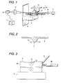
- FIG. 1 is a typical view of an optical fiber arrangement portion according to the invention, showing hone to assemble it.
- FIG. 2 is a front view of an optical fiber, showing the structure thereof.
- FIG. 3 is a front view of the optical fiber arrangement portion, showing how the optical fibers are arranged.
- FIG. 4 is a front view of a second embodiment of an optical fiber arrangement portion according to the invention.
- FIG. 5 is a front view of a third embodiment of an optical fiber arrangement portion according to the invention.
- FIG. 6 is a front view of a modification of the third embodiment of an optical fiber arrangement portion according to the invention.
- FIG. 7 is a schematic structural view of a conventional image forming apparatus.
- FIGS. 8A and 8B are explanatory views of the states of scanning lines formed on a photosensitive member.
- FIG. 9 is a front view of a conventional optical fiber arrangement portion.
- FIG. 1 is a typical view of the optical fiber arrangement portion 29 shown in FIG. 7, showing how to assemble it;
- FIG. 2 is a front view, of an optical fiber, showing the structure thereof; and,
- FIG. 3 is a front view of optical fibers, showing how they are arranged.
- a plate member 2 for holding an optical fiber 1 is disposed on the optical fiber 1 .
- the plate member 2 is made of, for example, a thin metal plate; and, as the material of the metal plate, there is used stainless steel, aluminum or iron. Also, the thickness of the plate member 2 is set such that, where the distance between the centers of the cores 12 of the optical fibers 1 in the optical fiber arrangement portion 29 is expressed as P and the clad diameter of the optical fiber 1 is expressed as D, the maximum thickness can satisfy P ⁇ D.
- P is 150 ⁇
- D is 125 ⁇
- the maximum thickness is 25 ⁇ ; and, therefore, there is used a stainless plate having a thickness of 20 ⁇ m.
- the plate member 2 can be bonded to the optical fiber 1 with ultraviolet hardening resin or adhesive.
- the plate member 2 is bonded to the optical fiber using ultraviolet hardening resin 14 .
- the ultraviolet hardening resin 14 is dropped down from a nozzle 15 onto the upper surface of a base member or the upper surface of the plate member 2 previously bonded to the optical fiber 1 .
- the positions of the optical fiber 1 and glass plate 3 are matched to each other.
- the vacuum attracting member 6 When the position matching operation is executed while holding the plate member 2 using the holding device 5 of a type that the vacuum attracting member 6 is mounted thereon, the vacuum attracting member 6 is contacted with the upper surface of the plate member of the optical fiber 1 , and a negative pressure is applied to the vacuum attracting member 6 to thereby attract and hold The plate member 2 .
- the vacuum attracting member 6 is a sucker-like attracting pad and, as the material of the vacuum attracting member 6 , there can be used rubber or resin; in fact, in most cases, rubber is used.
- the holding device 5 of a type that the thermally melting member (not shown) is mounted thereon As the thermally melting member, solder is attached to the holding device 5 , the holding device 5 with the solder attached thereto is contacted with the upper surface of the plate member 2 , heat is transmitted from the holding device 5 to the solder to thereby melt the same, so that the plate member 2 is soldering connected to the holding device 5 .
- the plate member 2 can be held by the holding device 5 .
- the plate member 2 can be separated from the holding device 5 .
- the plate member 2 of he optical fiber 1 is held using the holding device 5 including the former element, that is, the vacuum attracting member 6 .
- the light, which is emitted by a light emitting device 7 is guided into the optical fiber 1 from the end face thereof after the light is narrowed by a lens 8 ; the light, which is transmitted through the optical fiber 1 and is emitted from the core 12 that is situated on the opposite side of the optical fiber 1 , is observed from the back surface of the glass plate 3 by a monitor 11 which includes a magnifying lens 9 and a camera 10 ; and, the holding device 5 is moved to thereby adjust the position of the optical fiber 1 .
- the ultraviolet hardening resin 14 is dropped down into between the optical fiber 1 and glass plate 3 .
- the light including ultraviolet light rays is radiated onto the ultraviolet hardening resin 14 between the plate member 2 , optical fiber 1 and glass plate 3 to thereby harden the ultraviolet hardening resin 14 . Due to this, the optical fiber 1 , glass plate 3 and plate member 2 are bonded together.
- the ultraviolet hardening resin 14 dropped down onto the optical fiber 1 is allowed to flow down below the optical fiber 1 .
- the ultraviolet hardening resin 14 has no influence on an optical fiber 1 to be arranged next but rather reinforces the bonded portion of the previously bonded optical fiber 1 .
- adhesive can also be used instead of the ultraviolet hardening resin 14 , or bonding between the optical fiber 1 and glass plate 3 can also be achieved using laser welding.
- the optical fibers 1 each with two or more plate members 2 can be arranged vertically and thus there can be obtained a vertical optical fiber arrangement portion.
- a plurality of optical fibers 1 situated in the rear of the plate members 2 are bonded and fixed together using ultraviolet hardening resin (not shown) or adhesive (not shown).
- scanning lines can be formed at regular intervals on the photosensitive member 21 using a plurality of beams emitted from the optical fiber arrangement portion, which makes it possible to attain high-quality printing.
- FIG. 4 shows a second embodiment of an image forming apparatus according to the invention.
- the second embodiment is different from the first embodiment in that, to the optical fiber 1 , there is bonded a plate member which is formed by bonding a reinforcing member 18 formed of metal or glass to the plate member 2 according to the first embodiment using ultraviolet hardening resin (not shown) or adhesive (not shown)
- the optical fiber 1 and reinforcing member 18 are bonded to the glass plate 3 shown in FIG. 1 .
- the other remaining operations of the second embodiment are similar to those of the first embodiment. Thanks to the above, the bonding strength of the optical fiber 2 can be enhanced and thus a high-precision optical fiber arrangement portion can be obtained. Also, in case where an image is formed using the thus manufactured optical fiber arrangement portion, scanning lines can be formed at regular intervals on the photosensitive member 21 and also it can be confirmed that the printed image is of high quality.
- FIGS. 5 and 6 show a third embodiment of an image forcing apparatus according to the invention.
- a plate member 19 made 20 a glass plate or a metal plate, having a vertical end face and having a thickness equal to or smaller than the clad diameter of the optical fiber 1 , or a plate member 20 having an inclined end face and having the same thickness as the plate member 19 using ultraviolet hardening resin 14 or adhesive, or using laser welding; and, the plate member 19 or 20 is disposed horizontally with respect to the optical fiber 1 and is then held by the holding device 5 according to the first embodiment.
- an optical fiber arrangement portion in which a plurality of optical fibers are arranged with high precision, and thus there can be realized an image forming apparatus capable of high quality printing.
Abstract
Description
Claims (11)
Applications Claiming Priority (3)
| Application Number | Priority Date | Filing Date | Title |
|---|---|---|---|
| JP2000127356A JP2001311890A (en) | 2000-04-27 | 2000-04-27 | Image forming device |
| JPP.2000-127356 | 2000-04-27 | ||
| JP2000-127356 | 2000-04-27 |
Publications (2)
| Publication Number | Publication Date |
|---|---|
| US20010036346A1 US20010036346A1 (en) | 2001-11-01 |
| US6647189B2 true US6647189B2 (en) | 2003-11-11 |
Family
ID=18636967
Family Applications (1)
| Application Number | Title | Priority Date | Filing Date |
|---|---|---|---|
| US09/841,248 Expired - Fee Related US6647189B2 (en) | 2000-04-27 | 2001-04-25 | Image forming apparatus having an optical fiber array |
Country Status (2)
| Country | Link |
|---|---|
| US (1) | US6647189B2 (en) |
| JP (1) | JP2001311890A (en) |
Citations (6)
| Publication number | Priority date | Publication date | Assignee | Title |
|---|---|---|---|---|
| US3950074A (en) * | 1973-11-07 | 1976-04-13 | Minolta Camera Kabushiki Kaisha | Image-transmitting light-conducting fibre array |
| US4046454A (en) * | 1976-05-18 | 1977-09-06 | Bell Telephone Laboratories, Incorporated | Optical fiber connector |
| US4991930A (en) * | 1989-11-22 | 1991-02-12 | Eastman Kodak Company | Fiber optic array |
| JPH08222806A (en) | 1995-02-10 | 1996-08-30 | Hitachi Koki Co Ltd | Optical fiber coupling optical system |
| JPH10113832A (en) | 1996-10-09 | 1998-05-06 | Tokyo Parts Ind Co Ltd | Manufacture of dynamic pressure fluid beaking |
| US6330019B1 (en) * | 1998-11-13 | 2001-12-11 | Matsushita Graphic Communication Systems, Inc. | Image recording apparatus and optical recording head |
-
2000
- 2000-04-27 JP JP2000127356A patent/JP2001311890A/en active Pending
-
2001
- 2001-04-25 US US09/841,248 patent/US6647189B2/en not_active Expired - Fee Related
Patent Citations (6)
| Publication number | Priority date | Publication date | Assignee | Title |
|---|---|---|---|---|
| US3950074A (en) * | 1973-11-07 | 1976-04-13 | Minolta Camera Kabushiki Kaisha | Image-transmitting light-conducting fibre array |
| US4046454A (en) * | 1976-05-18 | 1977-09-06 | Bell Telephone Laboratories, Incorporated | Optical fiber connector |
| US4991930A (en) * | 1989-11-22 | 1991-02-12 | Eastman Kodak Company | Fiber optic array |
| JPH08222806A (en) | 1995-02-10 | 1996-08-30 | Hitachi Koki Co Ltd | Optical fiber coupling optical system |
| JPH10113832A (en) | 1996-10-09 | 1998-05-06 | Tokyo Parts Ind Co Ltd | Manufacture of dynamic pressure fluid beaking |
| US6330019B1 (en) * | 1998-11-13 | 2001-12-11 | Matsushita Graphic Communication Systems, Inc. | Image recording apparatus and optical recording head |
Also Published As
| Publication number | Publication date |
|---|---|
| JP2001311890A (en) | 2001-11-09 |
| US20010036346A1 (en) | 2001-11-01 |
Similar Documents
| Publication | Publication Date | Title |
|---|---|---|
| KR101152226B1 (en) | Projection and exposure apparatus | |
| US6330017B1 (en) | Light emitting diode array head including focusing lenses | |
| JPH03501782A (en) | optical fiber array | |
| JPH03504649A (en) | How to manufacture fiber optic arrays | |
| US5006201A (en) | Method of making a fiber optic array | |
| US20100001296A1 (en) | Light-emitting element array with micro-lenses and optical writing head | |
| US4991930A (en) | Fiber optic array | |
| KR20040095183A (en) | Projection and exposure apparatus | |
| JPH11216901A (en) | Optical print head | |
| KR20040095186A (en) | Projection and exposure apparatus | |
| US6647189B2 (en) | Image forming apparatus having an optical fiber array | |
| JPH04309916A (en) | Optical lens holding device | |
| KR100629209B1 (en) | Laser apparatus, exposure head, exposure apparatus and method of connecting optical fiber | |
| JPH09184997A (en) | Optical scanning device and its lens adjusting method | |
| JP2001027713A (en) | Optical transmission body array and its manufacture, and led printer and scanner | |
| JP4098918B2 (en) | Image recording device | |
| JPH08156320A (en) | Led printer head and manufacture thereof | |
| JP3663614B2 (en) | Multi-beam optical recording device | |
| JPS6262322A (en) | Optical printer | |
| TW565920B (en) | Light emitting element array module and printer head and micro-display using the same | |
| JP3707068B2 (en) | Multi-beam optical recording device | |
| JP4051565B2 (en) | Optical waveguide module of optical waveguide type optical recording apparatus | |
| US20060098432A1 (en) | Light source for image writing device, and production method for light source | |
| JP2001324690A (en) | Array light source | |
| JP2002267980A (en) | Optical fiber array recording device |
Legal Events
| Date | Code | Title | Description |
|---|---|---|---|
| AS | Assignment |
Owner name: HITACHI KOKI CO., LTD., JAPAN Free format text: ASSIGNMENT OF ASSIGNORS INTEREST;ASSIGNORS:YOKOSUKA, MICHIO;KATAOKA, KEIJI;REEL/FRAME:011759/0903 Effective date: 20010410 |
|
| AS | Assignment |
Owner name: HITACHI PRINTING SOLUTIONS, LTD., JAPAN Free format text: ASSIGNMENT OF ASSIGNORS INTEREST;ASSIGNOR:HITACHI KOKI CO., LTD.;REEL/FRAME:013782/0231 Effective date: 20030120 |
|
| FEPP | Fee payment procedure |
Free format text: PAYOR NUMBER ASSIGNED (ORIGINAL EVENT CODE: ASPN); ENTITY STATUS OF PATENT OWNER: LARGE ENTITY |
|
| FPAY | Fee payment |
Year of fee payment: 4 |
|
| FEPP | Fee payment procedure |
Free format text: PAYER NUMBER DE-ASSIGNED (ORIGINAL EVENT CODE: RMPN); ENTITY STATUS OF PATENT OWNER: LARGE ENTITY Free format text: PAYOR NUMBER ASSIGNED (ORIGINAL EVENT CODE: ASPN); ENTITY STATUS OF PATENT OWNER: LARGE ENTITY |
|
| REMI | Maintenance fee reminder mailed | ||
| LAPS | Lapse for failure to pay maintenance fees | ||
| STCH | Information on status: patent discontinuation |
Free format text: PATENT EXPIRED DUE TO NONPAYMENT OF MAINTENANCE FEES UNDER 37 CFR 1.362 |
|
| FP | Lapsed due to failure to pay maintenance fee |
Effective date: 20111111 |