US6600563B1 - Optical resonance analysis system - Google Patents
Optical resonance analysis system Download PDFInfo
- Publication number
- US6600563B1 US6600563B1 US09/486,424 US48642400A US6600563B1 US 6600563 B1 US6600563 B1 US 6600563B1 US 48642400 A US48642400 A US 48642400A US 6600563 B1 US6600563 B1 US 6600563B1
- Authority
- US
- United States
- Prior art keywords
- analysis system
- optical resonance
- resonance analysis
- illumination
- means further
- Prior art date
- Legal status (The legal status is an assumption and is not a legal conclusion. Google has not performed a legal analysis and makes no representation as to the accuracy of the status listed.)
- Expired - Lifetime
Links
- 230000003287 optical effect Effects 0.000 title claims abstract description 103
- 238000004458 analytical method Methods 0.000 title claims abstract description 94
- 238000005286 illumination Methods 0.000 claims abstract description 78
- 238000003384 imaging method Methods 0.000 claims abstract description 39
- 238000001514 detection method Methods 0.000 claims abstract description 21
- 238000002198 surface plasmon resonance spectroscopy Methods 0.000 claims description 39
- 238000002347 injection Methods 0.000 claims 5
- 239000007924 injection Substances 0.000 claims 5
- 239000000523 sample Substances 0.000 description 63
- 238000000034 method Methods 0.000 description 52
- 239000006185 dispersion Substances 0.000 description 23
- 238000010168 coupling process Methods 0.000 description 21
- 238000005859 coupling reaction Methods 0.000 description 19
- 230000008901 benefit Effects 0.000 description 18
- 230000008878 coupling Effects 0.000 description 18
- 229910052751 metal Inorganic materials 0.000 description 17
- 239000002184 metal Substances 0.000 description 16
- 230000008859 change Effects 0.000 description 15
- 230000033001 locomotion Effects 0.000 description 14
- 238000005259 measurement Methods 0.000 description 14
- 239000000463 material Substances 0.000 description 12
- 238000013461 design Methods 0.000 description 11
- 238000003556 assay Methods 0.000 description 10
- 230000000875 corresponding effect Effects 0.000 description 10
- 239000010408 film Substances 0.000 description 10
- 239000007789 gas Substances 0.000 description 10
- 230000035945 sensitivity Effects 0.000 description 10
- 230000005540 biological transmission Effects 0.000 description 9
- 239000010410 layer Substances 0.000 description 8
- 108020004414 DNA Proteins 0.000 description 7
- 238000003491 array Methods 0.000 description 7
- 239000003989 dielectric material Substances 0.000 description 7
- 230000000694 effects Effects 0.000 description 7
- VYPSYNLAJGMNEJ-UHFFFAOYSA-N Silicium dioxide Chemical compound O=[Si]=O VYPSYNLAJGMNEJ-UHFFFAOYSA-N 0.000 description 6
- 238000004364 calculation method Methods 0.000 description 6
- 239000007787 solid Substances 0.000 description 6
- 239000000758 substrate Substances 0.000 description 6
- 230000027455 binding Effects 0.000 description 5
- 239000011521 glass Substances 0.000 description 5
- 238000003801 milling Methods 0.000 description 5
- 230000010287 polarization Effects 0.000 description 5
- XUIMIQQOPSSXEZ-UHFFFAOYSA-N Silicon Chemical compound [Si] XUIMIQQOPSSXEZ-UHFFFAOYSA-N 0.000 description 4
- GWEVSGVZZGPLCZ-UHFFFAOYSA-N Titan oxide Chemical compound O=[Ti]=O GWEVSGVZZGPLCZ-UHFFFAOYSA-N 0.000 description 4
- 238000010521 absorption reaction Methods 0.000 description 4
- 230000002596 correlated effect Effects 0.000 description 4
- 238000005516 engineering process Methods 0.000 description 4
- 238000009396 hybridization Methods 0.000 description 4
- 238000012986 modification Methods 0.000 description 4
- 230000004048 modification Effects 0.000 description 4
- 108090000623 proteins and genes Proteins 0.000 description 4
- 229910052710 silicon Inorganic materials 0.000 description 4
- 239000010703 silicon Substances 0.000 description 4
- 238000005102 attenuated total reflection Methods 0.000 description 3
- 230000008033 biological extinction Effects 0.000 description 3
- 210000004027 cell Anatomy 0.000 description 3
- 238000006243 chemical reaction Methods 0.000 description 3
- 150000001875 compounds Chemical class 0.000 description 3
- 238000012937 correction Methods 0.000 description 3
- 238000001914 filtration Methods 0.000 description 3
- PCHJSUWPFVWCPO-UHFFFAOYSA-N gold Chemical compound [Au] PCHJSUWPFVWCPO-UHFFFAOYSA-N 0.000 description 3
- 229910052737 gold Inorganic materials 0.000 description 3
- 239000010931 gold Substances 0.000 description 3
- 210000003128 head Anatomy 0.000 description 3
- 239000007788 liquid Substances 0.000 description 3
- 238000004519 manufacturing process Methods 0.000 description 3
- 150000002739 metals Chemical class 0.000 description 3
- 239000004033 plastic Substances 0.000 description 3
- 229920000642 polymer Polymers 0.000 description 3
- 102000004169 proteins and genes Human genes 0.000 description 3
- 238000005070 sampling Methods 0.000 description 3
- 238000001228 spectrum Methods 0.000 description 3
- 239000010409 thin film Substances 0.000 description 3
- WSMQKESQZFQMFW-UHFFFAOYSA-N 5-methyl-pyrazole-3-carboxylic acid Chemical compound CC1=CC(C(O)=O)=NN1 WSMQKESQZFQMFW-UHFFFAOYSA-N 0.000 description 2
- RZVAJINKPMORJF-UHFFFAOYSA-N Acetaminophen Chemical compound CC(=O)NC1=CC=C(O)C=C1 RZVAJINKPMORJF-UHFFFAOYSA-N 0.000 description 2
- JBRZTFJDHDCESZ-UHFFFAOYSA-N AsGa Chemical compound [As]#[Ga] JBRZTFJDHDCESZ-UHFFFAOYSA-N 0.000 description 2
- 108090001008 Avidin Proteins 0.000 description 2
- 108091003079 Bovine Serum Albumin Proteins 0.000 description 2
- 241000283707 Capra Species 0.000 description 2
- RTZKZFJDLAIYFH-UHFFFAOYSA-N Diethyl ether Chemical compound CCOCC RTZKZFJDLAIYFH-UHFFFAOYSA-N 0.000 description 2
- 229910001218 Gallium arsenide Inorganic materials 0.000 description 2
- -1 ITO Substances 0.000 description 2
- 108060003951 Immunoglobulin Proteins 0.000 description 2
- 241000283973 Oryctolagus cuniculus Species 0.000 description 2
- 239000004793 Polystyrene Substances 0.000 description 2
- 229910052581 Si3N4 Inorganic materials 0.000 description 2
- 229910020442 SiO2—TiO2 Inorganic materials 0.000 description 2
- 108010090804 Streptavidin Proteins 0.000 description 2
- 239000004809 Teflon Substances 0.000 description 2
- 229920006362 Teflon® Polymers 0.000 description 2
- 229910052782 aluminium Inorganic materials 0.000 description 2
- XAGFODPZIPBFFR-UHFFFAOYSA-N aluminium Chemical compound [Al] XAGFODPZIPBFFR-UHFFFAOYSA-N 0.000 description 2
- 230000003466 anti-cipated effect Effects 0.000 description 2
- 230000009830 antibody antigen interaction Effects 0.000 description 2
- 239000000427 antigen Substances 0.000 description 2
- 102000036639 antigens Human genes 0.000 description 2
- 108091007433 antigens Proteins 0.000 description 2
- 201000009310 astigmatism Diseases 0.000 description 2
- 229940098773 bovine serum albumin Drugs 0.000 description 2
- 238000004422 calculation algorithm Methods 0.000 description 2
- 238000000576 coating method Methods 0.000 description 2
- 238000002474 experimental method Methods 0.000 description 2
- 238000000605 extraction Methods 0.000 description 2
- 239000005350 fused silica glass Substances 0.000 description 2
- 102000018358 immunoglobulin Human genes 0.000 description 2
- 230000003993 interaction Effects 0.000 description 2
- 230000002452 interceptive effect Effects 0.000 description 2
- 238000012417 linear regression Methods 0.000 description 2
- GQYHUHYESMUTHG-UHFFFAOYSA-N lithium niobate Chemical compound [Li+].[O-][Nb](=O)=O GQYHUHYESMUTHG-UHFFFAOYSA-N 0.000 description 2
- 230000007246 mechanism Effects 0.000 description 2
- 238000002156 mixing Methods 0.000 description 2
- 238000012544 monitoring process Methods 0.000 description 2
- ZKATWMILCYLAPD-UHFFFAOYSA-N niobium pentoxide Inorganic materials O=[Nb](=O)O[Nb](=O)=O ZKATWMILCYLAPD-UHFFFAOYSA-N 0.000 description 2
- URLJKFSTXLNXLG-UHFFFAOYSA-N niobium(5+);oxygen(2-) Chemical compound [O-2].[O-2].[O-2].[O-2].[O-2].[Nb+5].[Nb+5] URLJKFSTXLNXLG-UHFFFAOYSA-N 0.000 description 2
- BPUBBGLMJRNUCC-UHFFFAOYSA-N oxygen(2-);tantalum(5+) Chemical compound [O-2].[O-2].[O-2].[O-2].[O-2].[Ta+5].[Ta+5] BPUBBGLMJRNUCC-UHFFFAOYSA-N 0.000 description 2
- 238000001139 pH measurement Methods 0.000 description 2
- 229920002223 polystyrene Polymers 0.000 description 2
- 230000008569 process Effects 0.000 description 2
- 239000005297 pyrex Substances 0.000 description 2
- 239000010453 quartz Substances 0.000 description 2
- 230000002829 reductive effect Effects 0.000 description 2
- 229910052594 sapphire Inorganic materials 0.000 description 2
- 239000010980 sapphire Substances 0.000 description 2
- 239000004065 semiconductor Substances 0.000 description 2
- 230000011664 signaling Effects 0.000 description 2
- 238000004088 simulation Methods 0.000 description 2
- 238000001179 sorption measurement Methods 0.000 description 2
- PBCFLUZVCVVTBY-UHFFFAOYSA-N tantalum pentoxide Inorganic materials O=[Ta](=O)O[Ta](=O)=O PBCFLUZVCVVTBY-UHFFFAOYSA-N 0.000 description 2
- 230000026683 transduction Effects 0.000 description 2
- 238000010361 transduction Methods 0.000 description 2
- 238000013519 translation Methods 0.000 description 2
- 238000012935 Averaging Methods 0.000 description 1
- 108020004635 Complementary DNA Proteins 0.000 description 1
- 229910000530 Gallium indium arsenide Inorganic materials 0.000 description 1
- 239000000232 Lipid Bilayer Substances 0.000 description 1
- 241000282345 Meles Species 0.000 description 1
- 108091028043 Nucleic acid sequence Proteins 0.000 description 1
- BQCADISMDOOEFD-UHFFFAOYSA-N Silver Chemical compound [Ag] BQCADISMDOOEFD-UHFFFAOYSA-N 0.000 description 1
- 238000000862 absorption spectrum Methods 0.000 description 1
- 239000003463 adsorbent Substances 0.000 description 1
- 230000004075 alteration Effects 0.000 description 1
- 230000009286 beneficial effect Effects 0.000 description 1
- 230000015572 biosynthetic process Effects 0.000 description 1
- 239000012496 blank sample Substances 0.000 description 1
- 230000008499 blood brain barrier function Effects 0.000 description 1
- 210000001218 blood-brain barrier Anatomy 0.000 description 1
- 238000010804 cDNA synthesis Methods 0.000 description 1
- 210000000170 cell membrane Anatomy 0.000 description 1
- 229910052681 coesite Inorganic materials 0.000 description 1
- 239000002299 complementary DNA Substances 0.000 description 1
- 238000007796 conventional method Methods 0.000 description 1
- 238000001816 cooling Methods 0.000 description 1
- 229910052906 cristobalite Inorganic materials 0.000 description 1
- 238000013480 data collection Methods 0.000 description 1
- 230000001419 dependent effect Effects 0.000 description 1
- 238000011161 development Methods 0.000 description 1
- 230000018109 developmental process Effects 0.000 description 1
- 201000010099 disease Diseases 0.000 description 1
- 208000037265 diseases, disorders, signs and symptoms Diseases 0.000 description 1
- 238000006073 displacement reaction Methods 0.000 description 1
- 238000010494 dissociation reaction Methods 0.000 description 1
- 230000005593 dissociations Effects 0.000 description 1
- 239000003814 drug Substances 0.000 description 1
- 229940079593 drug Drugs 0.000 description 1
- 238000007877 drug screening Methods 0.000 description 1
- 230000005684 electric field Effects 0.000 description 1
- 238000004049 embossing Methods 0.000 description 1
- 230000005284 excitation Effects 0.000 description 1
- 230000004907 flux Effects 0.000 description 1
- 239000003574 free electron Substances 0.000 description 1
- 239000007792 gaseous phase Substances 0.000 description 1
- 238000012252 genetic analysis Methods 0.000 description 1
- 230000012010 growth Effects 0.000 description 1
- 230000002209 hydrophobic effect Effects 0.000 description 1
- 230000004941 influx Effects 0.000 description 1
- 230000010354 integration Effects 0.000 description 1
- 238000005468 ion implantation Methods 0.000 description 1
- 238000002955 isolation Methods 0.000 description 1
- 230000000670 limiting effect Effects 0.000 description 1
- 150000002632 lipids Chemical class 0.000 description 1
- 239000004973 liquid crystal related substance Substances 0.000 description 1
- 239000007791 liquid phase Substances 0.000 description 1
- 238000004949 mass spectrometry Methods 0.000 description 1
- 239000011159 matrix material Substances 0.000 description 1
- 239000012528 membrane Substances 0.000 description 1
- 239000007769 metal material Substances 0.000 description 1
- 230000009149 molecular binding Effects 0.000 description 1
- 238000005232 molecular self-assembly Methods 0.000 description 1
- 230000036961 partial effect Effects 0.000 description 1
- 239000000575 pesticide Substances 0.000 description 1
- 239000012071 phase Substances 0.000 description 1
- 229920002120 photoresistant polymer Polymers 0.000 description 1
- 238000007781 pre-processing Methods 0.000 description 1
- 230000001737 promoting effect Effects 0.000 description 1
- 230000001902 propagating effect Effects 0.000 description 1
- 210000001747 pupil Anatomy 0.000 description 1
- 230000005855 radiation Effects 0.000 description 1
- 230000035484 reaction time Effects 0.000 description 1
- 239000013074 reference sample Substances 0.000 description 1
- 238000011160 research Methods 0.000 description 1
- 230000002441 reversible effect Effects 0.000 description 1
- 238000000926 separation method Methods 0.000 description 1
- 239000000377 silicon dioxide Substances 0.000 description 1
- 229910052709 silver Inorganic materials 0.000 description 1
- 239000004332 silver Substances 0.000 description 1
- 230000003595 spectral effect Effects 0.000 description 1
- 238000004611 spectroscopical analysis Methods 0.000 description 1
- 229910052682 stishovite Inorganic materials 0.000 description 1
- 239000002344 surface layer Substances 0.000 description 1
- 238000003786 synthesis reaction Methods 0.000 description 1
- 238000012360 testing method Methods 0.000 description 1
- 231100000027 toxicology Toxicity 0.000 description 1
- 229910052905 tridymite Inorganic materials 0.000 description 1
- 239000012855 volatile organic compound Substances 0.000 description 1
Images


Classifications
-
- G—PHYSICS
- G01—MEASURING; TESTING
- G01N—INVESTIGATING OR ANALYSING MATERIALS BY DETERMINING THEIR CHEMICAL OR PHYSICAL PROPERTIES
- G01N21/00—Investigating or analysing materials by the use of optical means, i.e. using sub-millimetre waves, infrared, visible or ultraviolet light
- G01N21/75—Systems in which material is subjected to a chemical reaction, the progress or the result of the reaction being investigated
- G01N21/77—Systems in which material is subjected to a chemical reaction, the progress or the result of the reaction being investigated by observing the effect on a chemical indicator
- G01N21/7703—Systems in which material is subjected to a chemical reaction, the progress or the result of the reaction being investigated by observing the effect on a chemical indicator using reagent-clad optical fibres or optical waveguides
-
- G—PHYSICS
- G01—MEASURING; TESTING
- G01N—INVESTIGATING OR ANALYSING MATERIALS BY DETERMINING THEIR CHEMICAL OR PHYSICAL PROPERTIES
- G01N21/00—Investigating or analysing materials by the use of optical means, i.e. using sub-millimetre waves, infrared, visible or ultraviolet light
- G01N21/17—Systems in which incident light is modified in accordance with the properties of the material investigated
- G01N21/55—Specular reflectivity
- G01N21/552—Attenuated total reflection
- G01N21/553—Attenuated total reflection and using surface plasmons
Definitions
- This invention relates generally to optical resonance analysis systems, specifically to certain sensor design aspects and to analysis systems comprising illumination and detection systems that utilize those sensors for analysis
- Sensors can be described as being composed of two parts; the transducer and the active site.
- the transducer is defined as the part of the device that is capable of reporting change in its environment.
- Transducers can operate in several different modes but the most common are optical based devices. Examples of optical based transducers include surface plasmon resonance (SPR) devices and planar waveguide devices and grating coupled waveguide devices. These types of sensors are described in U.S. Pat. Nos. 4,882,288, 4931,384, 4,992,385, and 5,118,608 all incorporated by reference.
- the sensor may consist of a single analysis site, a one dimensional or linear array of analysis sites or a two dimensional array of analysis sites.
- Surface plasmon which exists at the boundary between metal and dielectric, represents a mode of surface charge vibrations.
- the surface charge vibration is the vibration of the electrons on the metal surface generated by exterior light, these electrons behaving like free electrons.
- the surface plasmon wave extends into space or dielectrics as an evanescent wave and travels along the surface.
- the plasmon field satisfies the Maxwell equations and boundary conditions for p-polarized radiation. This boundary condition requires that the dielectric constants of metal and dielectrics have opposite sign. Since the common dielectric compound has a positive dielectric constant, the plasmon exists in the frequency region of the metal where the dielectric constant is negative.
- the plasmon frequency is about 5, 4 or 15 eV, respectively, resulting in a plasmon wave being available in a frequency range covering WV, Visible and Infrared regions.
- the wave vector of the surface plasmon is larger than that of the exterior light, the exterior light cannot interact directly with surface plasmon.
- Utilization of the surface plasmon becomes possible when the exterior light wave is coupled with the surface plasmon by means of a grating or prism. These optical components provide an additional wave vector component to the exterior light, enabling energy exchange between the exterior light and the surface plasmon.
- the plasmon on the metal grating can interact with the exterior light by picking up an additional transverse momentum defined by the period of the structure.
- Attenuated total reflection in a high refractive index material such as a prism provides additional transverse momentum so that the exterior wave has a wave vector larger than the vacuum wave vector, and the wave vector in the prism is large enough to match to the plasmon wave vector.
- the prism method has been frequently utilized to determine optical constants of metals, because the resonance condition changes by the change in the refractive index.
- gratings play an important role in promoting the surface plasmon, this in turn means that the surface plasmon causes some anomalies to grating performance.
- theory of surface plasmons was also developed by grating scientists.
- the SPR type device basically measures refractive index changes in a thin 1 ⁇ m evanescent field zone at its surface.
- the active surface defines the application and the specificity of the transducer.
- Various types of surface modifications can be used, for example, polymer coated transducers can be used to measure volatile organic compounds, bound proteins can be used to look for trace amounts of pesticides or other interactive molecules, DNA can be used to look for the presence of complementary DNA or even compounds that bind unique DNA sites.
- Specific sensors can be obtained by generating arrays of specific DNA sequences that hybridize the sample DNA. This technique is commonly referred to as array hybridization.
- This type of sensor can operate in a gas or a liquid environment, as long as its performance is not degraded. Temperature range is selected by the application and should be controlled to better than 0.1° C. for maximum sensitivity measurements.
- Arrays have been built using fluorescence as the reporter but technologies such as SPR may be used resulting in reduced hardware cost, and greater generality.
- SPR is especially appropriate in monitoring the binding of combinatorial products because these products will not all have labels or properties such as fluorescence that one could monitor.
- An extension of surface plasmon resonance is the ability to combine this technique with others such as mass spectrometry. An example would be if a signal is detected on the SPR sensors indicating binding, a second technique could be used to identify the bound material.
- K x and D represent the wave vector in the x-direction and the angular frequency of the wave, respectively.
- x and t are distance and time, respectively.
- the plasmon wave vector is given by
- ⁇ 0 and ⁇ 1 are dielectric constants of dielectric compound and metal and ⁇ is the wavelength of the exterior light. Twice the imaginary part of K x , 2K xi , determines the distance the plasmon electric field decays to 1/e along the metal surface.
- Gratings provide the standing wave vector parallel to the boundary depending on the groove space and order of the grating.
- resonance absorption occurs when the exterior light wave vector component in the boundary plus the grating vector equal to the plasmon vector as given by
- a and m are the groove spacing and the order of grating.
- Term ⁇ is the incident angle of the exterior light.
- the SPR wavevector K x corresponding to a given frequency ⁇ can be estimated as given in eq (1).
- k sp the real part of the center wavevector of the plasmon.
- the Lorentzian full width at half maximum, in the absence of radiative coupling, is given by twice the imaginary part of the wavevector, k i .
- ⁇ is the vacuum wavelength
- ⁇ is the input angle in air (not in the sample medium)
- m is the integer grating coupling order
- a is the grating groove pitch.
- n is the refractive index of the coupling prism and ⁇ P is the input coupling angle within the prism medium.
- the in-air angular resonance widths are nearly the same.
- the full FWHM angular width in air, for either case, is found from doubling (10) or (13) to be
- the plasmon wavevector must change to k′ sp such that
- the partial ⁇ k/ ⁇ is calculated numerically from (1) using tabulated dielectric constant data for the materials forming the SPR device. Note that in general, it is negative.
- Waveguide sensors consist of one or more layers of dielectric materials coated with a thin film of material of higher index of refraction.
- the waveguide sensor responds to: changes in the refractive index n C of the cover medium C; adsorption of molecules out of a gaseous or liquid phase cover, to form a surface layer of thickness dr and refraction index n F . and, if used as dispersing element (Propagation angle in the waveguide depends on the wavelength), it can record the absorption spectrum of molecules on the surface.
- the sensitivity can be expressed as the change in the effective index of refraction N (of a guided mode TE or TM) in cases 1-3. In the case of absorption measurements (and using the guide as a dispersive element) the sensitivity is determined by the minimum detectable absorption.
- Waveguide films include SiO 2 , SiO 2 —TiO 2 , TiO 2 , Si 3 N 4 , lithium niobate, lithium tantalate, tantalum pentoxide, niobium pentoxide, GaAs, GaAlAs, GaAsP, GaInAs, and polymers (polystyrene).
- Waveguide film thickness is usually in the range of 100-200 nm.
- Example ranges of indexes of refraction include from 1.4-2.1.
- Chemoselective coatings can be placed on the waveguide film surface. Light coupling into the waveguide can be achieved by using surface relief gratings or prisms.
- a way to measure the changes in the effective index is by the change in the angle at which the mode exits from the waveguide. This can be done by an array detector, which at the same time can measure the intensity at each wavelength. In that case the time of measurement is typically 100-200 ⁇ sec.
- Associated system components usually include gratings (to match the Dangle dispersion curve of the waveguide), mirrors, lenses, polarizers, white light sources, and array detectors.
- Possible applications are analytical chemistry, humidity and gas sensing, PH measurement, bio- and immuno-sensor applications, molecular recognition in biology, signaling transduction between and within cells, affinity of biotinylated molecules (bovine serum albumin) to Avidin or strept-Avidin, antigen-antibody interactions (immunobinding of rabbit/goat anti-h-IgG antibody to the human immunoglobulin h-IgG antigen) etc.
- the grating coupled waveguide sensor can measure the number, size and shape of living cells growing on its surface, in real time and non-invasively. Applications include toxicology and cancer research, pharmacology—drug determination.
- a waveguide supported lipid bilayer is the closest to real cell membrane simulation, and can be used for drug screening as well as blood-brain barriers.
- Waveguides can be used to analyze properties of bilayer lipid membranes (BLM) and other thin films, to measure protein-BLM interaction, and the thickness, density, anisotropy, and the reaction of thin films to perturbations in time.
- BBM bilayer lipid membranes
- Other applications include using long DNA molecules as a surface coat to measure hybridization and protein binding, molecular self-assembly, nanoscience, and analysis of association and dissociation kinetics.
- Grating couplers are used for efficient coupling of light into or out of a waveguide that consists of one or more layers of dielectric materials. At the same time they can be used for measuring the effective index of refraction N of all possible TE and TM modes.
- the primary sensor effect is a change ⁇ N in the effective refractive index N of the guided modes induced by the adsorption or binding of molecules from a sample on the waveguide surface. From ⁇ N it is possible to calculate the refractive index, thickness and surface coverage of the adsorbed or bound adlayers.
- ⁇ N is measured only in the grating region which is where the sample should be placed. With optimal grating design a coupling efficiency of the order of 45-90% can be achieved.
- a grating coupler can operate in a gas or a liquid environment, as long as its perfomance is not degraded. Temperature range is selected by the application and should be controlled to better than 0.1° C. for maximum sensitivity measurements.
- Substrates include sapphire, ITO, fused silica, glass (Pyrex, Quartz,), plastic, teflon, metal, and semiconductor materials (Silicon).
- Waveguide films include Sio 2 , SiO 2 —TiO 2 , TiO 2 , Si 3 N 4 , lithium niobate, lithium tantalate, tantalum pentoxide, niobium pentoxide, GaAs, GaAIAs, GaAsP, GalnAs, and polymers (polystyrene).
- Waveguide film thickness can be in the range of 100-200 nm and indexes of refraction can be in the range of 1.4-2.1.
- Gratings can be made by embossing, ion-implantation and photoresist techniques, on the substrate or in the waveguide film. Typical numbers are 1200-2400 lines/mm, 2 ⁇ 16 mm in size and 1:1 aspect ratio (20 nm features). Chemoselective coatings can be placed on the waveguide film surface.
- mechanical angle scanning measurement time is typically 2-3 sec. If an array of sources is used in conjunction with a lens this time is shortened.
- Associated system components usually include optics, mirrors, lenses, polarizers, light sources, light source arrays, laser sources, single or position sensitive detectors, rotation stages, and stepper motors
- Applications include analytical chemistry, humidity and gas sensing, PH measurement, bio- and immuno-sensor applications, molecular recognition in biology, signaling transduction between and within cells, affinity of biotinylated molecules (bovine serum albumin) to Avidin or strept-Avidin), antigen-antibody interactions (immunobinding of rabbit/goat anti-h-IgG antibody to the human immunoglobulin h-IgG antigen) etc.
- biotinylated molecules bovine serum albumin
- Avidin or strept-Avidin Avidin or strept-Avidin
- antigen-antibody interactions immunobinding of rabbit/goat anti-h-IgG antibody to the human immunoglobulin h-IgG antigen
- SPR and waveguides typically include an illumination system having the capability to project light at various frequencies or angles onto the resonance device and a detection system for detecting the corresponding resonance peaks.
- the illumination systems are typically composed of a light source, a means for causing the light source to impinge on the sensor at different angles or at different frequencies, and optics to facilitate imaging the source onto the sensor.
- the choice of light source is based on the wavelength region required and the etendue (solid angle X photon flux) of the optical system.
- broadband or monochromatic sources to choose from, such as: incandescent, LED's, super luminescent diodes, lasers (fixed and tunable, diode, solid state, gas), gas discharge lamps (line and continuum), with or without filters.
- Wavelength scanning is usually accomplished by coupling the source with filter wheels, scanning monochrometers or acousto-optical tunable filters, or in the case of a laser source by using a tunable diode laser.
- Angle scanning is usually accomplished by mechanically positioning the source at a series of angles with relationship to the sensor. In addition the source must be oriented and focused so that it optimally projects onto the sensor.
- Light rays from the illumination system are reflected from the sensor with their angle of reflection equal to their angle of incidence.
- the rays will typically span a small range of angles in the perpendicular plane.
- the detector is typically positioned to optimally receive the rays coming from the sensor.
- Other important detector considerations are resolution, pixel size, number of pixels, the algorithms that will be used for analyzing the resonance wavelengths or angles, and the chemistry occurring on the detector.
- a peak or a dip is obtained over a sometime sloped baseline.
- this peak or dip will shift depending on the change in refractive index corresponding to concentration difference between the two samples.
- the concentration can then be predicted using a calibration model relating the peak or dip shift to concentration.
- This invention is directed toward an analysis system, comprising an illumination and detection system, which utilizes a surface plasmon device or a waveguide as a sensor.
- the invention is further directed toward an illumination system utilizing an array of light sources to facilitate angle or wavelength scanning.
- the invention is further directed toward a means for providing independent axial and rotational positioning of the array of light sources.
- the invention is further directed toward utilizing a diffraction grating or a diffractive optical element as a pre-dispersive or post-dispersive element in the analysis system allowing the use of low cost, broad band light sources.
- the invention is further directed toward an anamorphic optical design that allows the analysis system to generate and detect resonances, from a one dimensional array of sites on the same substrate, simultaneously.
- the invention further comprises a method for predicting concentrations using a calibration model relating the resonance peak shift to concentration.
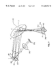
- FIG. 1 shows an embodiment of the invention.
- FIG. 2 shows an example of a one dimensional array of light sources.
- FIG. 3 shows an example of a two dimensional array of light sources.
- FIG. 4 shows a mechanism that allows independent axial and rotational movement of the source.
- FIGS. 5A, 5 B and 5 C show a cross sectional view of a slot at three points of operation of the axial and rotational mechanism.
- FIG. 6 shows resonance dispersion curves for various conditions.
- FIG. 7 and 8 show an additional embodiments of the invention using anamorphic imaging.
- FIG. 9 shows an additional embodiment of the invention.
- FIG. 1 shows an embodiment of the invention utilizing an angle scanning illumination system, a sensor with a two dimensional array of sites derivatised or sensitized with the same sample (for the analysis of multiple assays) or different samples (for the analysis of a single assay), and sequential detection.
- a light source 10 is mounted on a device 15 that allows independent axial and rotational movement. The light emitted from the source travels through a polarizer 20 , a filter 30 , a lens system 40 , a pre-dispersive grating 50 , and impinges on a sensor 60 . Light reflected from the sensor 60 then travels through an imaging lens 70 , an angle or wavelength stop 80 to a detector 90 .
- the source is constructed as shown in FIG. 3, a two dimensional array of sources 110 .
- the choice of light source is based on the wavelength region required and the etendue (solid angle X pupil area) of the optical system.
- the sensor resonance becomes sharper with increasing source wavelength.
- the advantage of having narrow resonance is in the ability to detect smaller shifts (sensitivity).
- the resonance decay length increases with wavelength and thus the reaction site dimensions have to increase (spatial resolution, and system throughput).
- broadband or monochromatic sources to choose from, such as: incandescent, LED's, super luminescent diodes, lasers (fixed and tunable, diode, solid state, gas), Gas discharge lamps (line and continuum), with or without filters.
- Incoherent sources are preferred in order to eliminate speckle noise.
- An example of a light source in this embodiment is a Hewlett-Packard HSDL-4400 LED emitting at 875 nm, where the resonance width is 0.3 degrees or 5 nm. At this wavelength the SPR decay length is of the order of 25 microns.
- each LED corresponds to a different angle of illumination.
- the source 10 is mounted on a device 15 that allows independent axial, or focusing, and rotational movement.
- the design and arrangement of this device assembly as shown in FIG. 4 allows the source to move freely and independently in the specified motions of rotation and focus, over the desired ranges. Additionally, the assembly is designed to be compatible with standard bayonet photographic lens mounting configurations.
- the design of the focusing motion components was intended to take advantage of the increased sensitivity of axial motion inherent in the application of rotational movement within helical patterned grooves, and the smooth, gradual effect of an inclined plane this interaction produces.
- the invention is directed to a method by which the helical slots 208 are formed in the stationary cylindrical housing 201 .
- the cylindrical housing 201 is mounted to the slide bed in a standard indexing head, with its cylindrical axis perpendicular to the axis of the tooling head.
- a slot saw of appropriate width and diameter is mounted in a common right angle fixture attached to the milling head, the arbor being parallel to the cylindrical axis of the housing, and the plane of the slot saw being perpendicular to the same.
- the right angle attachment is then rotated to a specified angle relative to the cylindrical axis of the housing.
- the center of the slot saw is positioned over the center of the housing using standard trigonometric methods.
- the slots 208 are then cut into the housing by raising the slide bed of the milling machine.
- the resulting slot 208 is considered pseudo-helical, that is, the sides of the slot are perpendicular to the cylindrical axis of the housing only at center point of the arc of the slot 208 as shown in FIG. 5 A.
- the loss of perpendicularity in the pseudo-helical slot 208 is compensated for, and true helical like motion in the slot is maintained, by using a connecting pin 205 with a smaller diameter than the width of the slot inserted into a ball 212 having an outside diameter equal to the width of the slot 208 .
- a connecting pin 205 with a smaller diameter than the width of the slot inserted into a ball 212 having an outside diameter equal to the width of the slot 208 .
- the conventional method of introducing true helical slots or grooves in a cylinder requires unique equipment and skills, but can produce features that can be of nearly unlimited length, depth and width, and that preserve the perpendicularity of the sides of the slots or grooves relative to the cylindrical axis at any point along the cut.
- FIG. 1 the source 10 is mounted on the device 15 .
- FIG. 4 shows the device 15 in detail consisting of a moveable, telescoping cylinder 200 within a stationary cylindrical housing 201 , which is designed at one end 215 to mount and lock to the conventional male bayonet mounting surface of many common photographic lenses.
- the housing is further adapted at the mounting end to accommodate typical optical elements like an interference filter.
- the source 10 is held securely within the moveable, telescoping cylinder 200 which can move axially (focus) and rotationally, along, and around the center axis of the stationary cylindrical housing 201 .
- Focus and rotation of the source 10 are controlled by external annular grip rings 204 and 216 respectively that fit around the outside diameter of the stationary cylindrical housing 201 , and are in contact with the moveable, telescoping cylinder 200 by way of pins 205 that connect the focus grip ring 204 and the moveable cylinder 200 through slots 208 in the stationary cylindrical housing 201 and that connect the rotational grip ring 216 and the movable cylinder 200 through the circumferengial slot 206 in the stationary cylindrical housing 201 .
- a slot in the stationary housing, for rotational control of the moveable cylinder, located opposite the mounting end and in the telescoping area of the housing, is a circumferengial through slot 206 T over a range of 180 degrees and an external counterbore groove 206 C for the remaining 180 degrees.
- Another circumferengial through slot 207 of at least 90 degrees range, that allows rotational control of a optical polarizer by way of a radial lever that extends from the polarizer, is located near the mounting end of the housing.
- Additional slots in the stationary housing, 208 for focus control of the moveable cylinder 200 are evenly spaced, pseudo-helical through slots, cut at an appropriate angle to the cylindrical axis of the stationary cylindrical housing 201 to provide the desired sensitivity and control of telescoping focus (axial) motion, and are located in the telescoping area of the housing between the mounting end 215 and the circumferengial through slot 206 for rotational control of the moveable cylinder.
- the moveable cylinder 200 has an appropriately long axial slot on its outer surface for rotational control, and is engaged to the rotational grip ring 216 , associated with the circumferengial through slot 206 T and the circumferengial groove 206 C, and is engaged to the focus grip ring 204 , associated with the pseudo-helical grooves 208 of the housing.
- the external grip rings 204 and 216 are designed to slip fit onto the outside diameter of the cylindrical housing 201 .
- Three equally spaced screw tapped holes 209 in each of the rings accept a threaded portion of the pins 205 that penetrate the cylindrical housing 201 and engage the moveable cylinder 200 in the appropriate slots and grooves.
- one pin 205 extends through the circumferengial slot 206 T of the cylindrical housing 201 and slidingly engages the axial slot 210 of the moveable cylinder 200 .
- An additional two pins extend through the rotational grip ring 216 into the external counterbore groove 206 C to provide stability and a means of locking its position.
- a more defined resonance is generated by ‘p’ polarized light impinging on the sensor.
- the amplitude of the resonance is inversely proportional to the extinction coefficient of the polarizer. Since the amplitude is large to start with (50-90%), a poor polarizer (0.1-0.01 extinction) is sufficient.
- Any of a number of devices including, linear polarizers, prism polarizers, polarizing beam splitters, retardation plates, Cornu pseudopolarizer, or Dichroic sheet polarizers can be used. As shown in FIG. 1 a dichroic linear film polarizer 20 with an extinction coefficient of 10- ⁇ circumflex over ( ) ⁇ 2, and 70% transmission @ 875 nm (Oriel 27361) is used for polarizing the light in the ‘p’ (II) direction.
- Scanning the illumination angle may be done with variety of devices and techniques such as a goniometer, source or slit translation, rotating mirror or refractor scanner, an LED/Laser diode array at the focus of a lens, or a spatial modulator. Angle scanning may also be accomplished by mechanically moving a single source element to different locations that result in the source impinging on the sensor at different angles.
- This embodiment uses an array of LED's as the source 10 located at the back focal plane of the lens system 40 .
- the array can be constructed with multiple tilted rows of LED's or straight rows and a tilted array, such that each LED is at a unique height above or below the optical axis, and with the center LED exactly on this axis.
- each diode produces a collimated beam illuminating the sensor at an angle which varies with the height of each LED relative to the optical axis.
- the range of angles in the beam, ⁇ ⁇ is given by the height of a diode divided by the focal length of the angle scanning lens system.
- the range of angles available is given by the height of the array divided by the focal length of the lens system 40 .
- the step size of the angle is given by the diode spacing divided by the focal length of the lens system 40 . Lateral displacements (sideways from the optical axis) will produce negligible resonance broadening.
- a Minolta 75-300 mm Zoom lens in combination with a Tamron 2 ⁇ teleconverter is used as the lens system.
- the sample has to be illuminated at a different resonance angle for each wavelength in the light source spectrum.
- the relationship between the wavelength and the angle defines the resonance dispersion curve.
- the slope of this curve is the resonance dispersion (R Disp ).
- a reflection grating as well as a transmission grating can be used; for a reflection grating, ⁇ i and ⁇ ° should be far apart, to allow the placement of additional optics without vignetting; for a transmission grating, any combination of angles will work; diffraction efficiency should be maximized for the polarization required by the resonance sample.
- the resonance peak is observed by scanning the illumination angle for each wavelength around the resonance angle.
- Line A describes a pre-dispersion grating designed to closely match a section of the dispersion curve at a particular index of refraction.
- FIG. 1 we measure the resonance simultaneously at all the points on line A, and in order to scan the resonance, the whole line can be shifted in angle (angle scan).
- angle scan angle scan
- FIG. 1 a 1200G/mm Kaiser Optics (HG-875-31-40) holographic transmission grating is used as the pre-dispersive grating 50 for dispersing the 830-910 nm wavelength range to match the resonance angles.
- the transmission of this grating for ‘p’ polarized light is around 90%.
- An 875 nm/10 nm(fwhm), 65% transmission interference filter 30 (Oriel 59495) is used for filtering off-resonance wavelength/angles portions of the source spectrum, to achieve a better dispersion matching, and narrower resonances.
- Lines B and C on FIG. 4 describe a pre-dispersion grating which does not compensate for sensor dispersion, but is useful for alternative embodiments (below).
- the advantage of this method is the coverage of a range of indices of refraction but at the expense of signal.
- the difference between B and C is in the range of angles and wavelengths that are covered by the pre-dispersion grating which in turn determines the requirements of the optical system that is used to image the sensor on the detector.
- the sensor shown in FIG. 1, 60 in this embodiment is a grating coupled surface plasmon device with a 854.5 nm groove spacing.
- a planar waveguide or multi-layer planar waveguide may also be used.
- a 2D array of sites derivatised/sensitized??? with the same sample can be used for the analysis of multiple assays.
- a 2D array of sites with different samples can be used for the analysis of a single assay
- light rays are usually reflected from the sensor 60 with their angle of reflection equal to their angle of incidence.
- the rays will typically span a small range of angles in the perpendicular plane, with the central angle to the sensor being ⁇ r .
- It is convenient to take the ray coming from the center of the sensor at an angle ⁇ T and ⁇ A 0 as the optical axis of the detection system.
- Imaging on the detector is obtained with a single, high quality, lens 70 oriented nearly normal to the optical axis and the detector making an angle of very nearly— ⁇ T with the optical axis.
- the entire system has a symmetry plane that is perpendicular to the orientation of the sensor.
- ⁇ T 14°
- ⁇ 0.49° the detector tilted ⁇ 14.08°
- This configuration allows an array of 100 by 100 samples on a 1 cm square sensor to be resolved.
- Another type of lens that can be utilized in this embodiment is Rolyn part number 22.0162, having a 60 mm focal length, and a 30 mm diameter. Using a ⁇ T of 5°, an array of 50 samples in the parallel direction, and 25 samples in the perpendicular direction on a 1 cm square sensor can be resolved.
- the size of the detector array can be minimized by demagnifying the image on it, but at the expense of a longer optical path than that for one-to-one imaging, and a larger diameter lens. Demagnification will also be limited by the need to have a length of at least a few pixels per sample for adequate resolution. Alternatively, the image can be magnified in order to get more pixels per imaged sample. Up to a certain point, a long focal length will make the optical path closer to paraxial and thus less demanding.
- the optical limitations on the sample density are image quality and pixel density.
- Imaging lens 70 may also be a curved mirror where a one dimensional array detector is used. The detector can be positioned so that the blurring along the line connecting the images of the individual sample bars is minimized so that any astigmatism will not have a significant effect.
- the resulting light/signal levels can be very low (compared to the detector and system noise levels).
- the preferred mode of operation in this case is to always be signal shot noise limited, which means that all the other system noise sources should be minimized.
- To increase the signal levels one can image a range of resonance wavelength/angle pairs on the detector, but that imposes the requirement of additional scanning.
- the electronic read noise can be minimized by the well known CDS (correlated-double sampling), and MPP (Multi-phase pulsing) electronics, and the use of ‘quiet’ electronic components.
- the digitization noise can be minimized by increasing the effective number of A/D bits, or by dithering and averaging the signal.
- a 30 frames per second, 10 bit, Kodak digital CCD camera can be used.
- This camera uses a 1K ⁇ 1K silicon CCD chip, and can fully image a 10 ⁇ 10 mm sensor at unity magnification.
- the quantum efficiency of the silicon CCD is about 10% @ 875 nm.
- the integration time of the camera should be chosen such that the pixel wells are nearly filled in that time (signal shot-noise limited), and the frame rate is chosen to match the chemical reaction time scale.
- the senor is illuminated with a beam of light having a sufficiently small range of angles at each wavelength such that it will generate a sharp resonance.
- the angle is scanned as a function of time so as to sequentially trace out the resonance for the different active sites having different values of the sample refractive index.
- the resonance refractive index thus varies monotonically during the scan.
- the sensor is imaged onto a detector that has dimensions corresponding to the sample array.
- the outputs of the detector pixels are recorded as a function of time.
- the pixels onto which this sample active site is imaged will show a decrease in intensity. From the parameters of the incident light and the detector intensities versus time, the resonance position and hence the effective index of refractive index for each sample in the array can be determined.
- the polarizer (???) is set such that the polarization of the light incident on the sensor is parallel to the sensor grating grooves (‘s’) such that no SPR is generated.
- the reflected intensity is recorded (in computer memory for example) for each element in the source array.
- the polarizer is set such that the polarization of the light incident on the sensor is perpendicular to the sensor grating grooves (‘p’) and an SPR is generated.
- the reflected intensity is measured and divided by the corresponding pre-recorded intensity. This results in a normalized resonance peak, which can be used for further quantitation.
- a dark exposure is recorded, when all the elements in the light source are turned off. This dark reading is subtracted from any other measurement.
- the read rate of the array is set relative to the scan rate of the illumination beam so as to take at least five to ten readings across a typical resonance.
- the scan rate of the illumination beam is set so that each reading of the array integrates enough light for adequate S/N without risking saturation.
- two dimensional array systems take better advantage of the available light than do one dimensional array systems.
- FIG. 8 shows an additional embodiment of the invention.
- the light source 10 in this embodiment comprises a light emitting element 370 and a collimating lens 360 .
- the light emitting element is an extended monochromatic or quasi-monochromatic source such as a filtered gas discharge lamp or a diffused laser diode.
- light from the source 10 is directed toward a sensor 60 over a range of angles sufficient to cover all possible resonance positions.
- the sensor surface is divided into a one dimensional array of active sites 300 , 310 , 320 .
- the light reflected from the active sites on the sensor on planes parallel to the x′′-z plane impinges on an anamorphic optical system 120 which then directs the light to a two dimensional detector array 90 .
- the focal length of the anamorphic imaging system is different in two orthogonal planes.
- Using this technique allows the system to image angles reflected from the sensor in the perpendicular plane, and the active site array in the parallel plane along the y axis.
- Active site 300 is imaged to zone 330 on the detector. Within this zone angles are displayed along the x′ axis on the detector 90 , Similarly site 310 is imaged to zone 340 and site 320 is imaged to zone 350 .
- the detector must be at the focal point of the imaging device in the perpendicular plane.
- the focal length of the imaging device in the parallel plane and the distance from it to the sensor are selected so that the sensor is imaged at the detector.
- the focal length in the parallel plane must be significantly less than that in the perpendicular plane.
- the anamorphic lens system 120 can be a single lens, a combination of a standard lens and a cylindrical lens, or a spherical mirror which has a natural astigmatism when used off axis. If, for example, the mirror is tipped at a 45° angle to the optical axis, about an axis in the perpendicular plane, as in FIG. 8, the focal length in the perpendicular (sagital) plane will be twice that in the parallel (tangential) plane.
- the corresponding resonance will move along the angle axis on the detector, ie along the x′ axis.
- FIG. 8A shows a similar embodiment, where source 10 comprises a polychromatic point source 400 , collimating lens 390 , and anti-correlation grating 380 .
- the anti-correlation grating produces a pre-dispersion corresponding to curve B in FIG. 6 .
- the different wavelengths in the bandwidth of source 400 impinge on the sensor 60 at angles which accentuate rather than compensate for the resonance dispersion in the sensor.
- resonance position shifts on the sensor 90 are enhanced over those of a simple wavelength or angle dispersive system.
- the entire set of sample resonances is captured in one array detector exposure. This improves resonance detection accuracy by eliminating effects of source fluctuations and/or system drifts.
- a peak is obtained that typically has a dip over a sometime sloped baseline. When the measurement is performed on another sample at a different concentration, this dip will shift depending on the change in refractive index corresponding to concentration difference between the two samples.
- the concentration can then be predicted using a calibration model relating the peak shift to concentration.
- the algorithm to be used for peak shift calculation using the two peaks calls for a model peak to begin.
- the model peak is an x-y pair representing the shape and location of a reference peak from which all actual peak locations are to be measured. This model peak can be obtained through theoretical calculation which has the advantage of being free from all baseline effects.
- the measured reference peak needs to be processed for noise and corrected for baseline effects, if necessary.
- the measured model peak can be smoothed through Savitzky-Golay digital filtering with a filter that is smaller than the resonance width to insure no peak distortion. If it is expected that the baseline of the reference peak will follow a different shape (e.g., a polynomial of different order) from that of an unknown peak, baseline correction needs to be performed on the reference peak by, for example, fitting a low order polynomial to both ends of the reference peak and subtracting it from the same peak.
- model peak The reference peak after this pre-processing (noise filtering and possibly baseline correction) is called model peak and will be used to determine the relative shift of an unknown peak.
- the first column is composed of ones to account for a vertical offset
- the second column is composed of the series 1, 2, . . . , m, to represent the tilt of a baseline
- the third column represents the model peak with intensities at m different wavelengths or angles
- the last column is the first derivative of the model peak which can be computed with a Savitzsky-Golay filter of proper order and size.
- the vector e (the same dimension as the unknown peak y) is the model error
- the first two coefficients (b 1 and b 2 ) in b represent the zeroth and first order terms for the baseline
- the third coefficient b 3 represents a relative scale in peak intensity (or attenuation) between the unknown and the reference sample.
- the shift of the unknown peak with respect to the model peak can be calculated by taking the ratio between the fourth and the third coefficient
- the shift thus calculated will be in units of wavelength or angle spacing in y (consistent with the unit with which the derivative is calculated). This shift in either wavelength or angle can then be related to sample concentration through a calibration procedure.
- the most computationally expensive part, (X T X) ⁇ 1 X T only needs to be calculated once and stored for repeated applications to successive unknown measurements y without re-computing it every time when an unknown sample is measured.
- the shift is large, for example, larger than 1 ⁇ 2 of the sampling interval, it may be necessary to refine the derivative calculation by pre-shifting the unknown peak y according to the first shift estimate so that it becomes closer to the model peak for a second and improved shift estimate.
- the pre-shifting can be accomplished through proper interpolation such as spline interpolation. It usually takes less than 5 iterations to achieve satisfactory shift estimation.
- FIG. 9 shows an embodiment of the invention directed toward wavelength scanning.
- Light emitted from the source 10 travels through an optical system 130 and impinges on a sensor 60 .
- Light reflected from the sensor 60 then travels the detector 90 .
- the wavelength scanning means may comprise the optical system 130 which may be a spectrometer, a grating, an acousto-optical tunable filter, a Fabrey-Perot or Fourier transform interferometer, a liquid crystal filter, a tilting dielectric filter, a linear variable filter, a Lyot filter, or a tunable laser.
- the wavelength scanning means may comprise the source 10 and the optical system 130 , where the source is a linear array as shown in FIG. 2 or a two dimensional array as shown in FIG. 3 and the individual elements of the array produce different wavelengths.
- the optical system 130 serves to focus the different wavelengths onto appropriate areas of the sensor.
- the light throughput will be proportional to the solid angle of the illumination beam, the wavelength increment from the monochromator, and the size of the sample sites.
- the solid angle of the illumination beam is pi times ⁇ T times ⁇ L (both in radians).
- ⁇ T in radians equals the monochromator slit width divided by the focal length of the imaging lens, L 1 .
- the wavelength range is the product of the slit width and the dispersion of the monochromator.
- ⁇ L in radians is the product of the focal length of lens L 1 and the slit height. This angle can be increased up to the point at which it degrades the imaging on the detector to the point where adjacent samples are insufficiently resolved.
- the grating of the monochromator is imaged onto the SPRG.
- the size of this image on the SPRG will be the size of the grating times the focal length of L 1 , divided by the length of the monochromator.
- step tunable is adequate as long as the minimum steps are not too large.
- Perpendicular plane refers to any of the planes which are perpendicular to the grating lines.
- Parallel plane refers to any of the planes which are parallel to both the grating lines and the optical axis.
- the angle of incidence of a ray on the grating is described in terms of two projections. ⁇ T is the angle of incidence in a perpendicular plane. This angle is typically 10° to 20°.
- ⁇ L is the angle of incidence in a perpendicular plane. This range of this angle is a few degrees which are centered on zero. The ranges of these angles incident on the sensor are ⁇ L and ⁇ T , respectively.
- the wavelength of the illuminating light is denoted ⁇ . It has a range of ⁇ .
- ⁇ L should have a relatively large value for good signal to noise. The limit on its range is insufficient resolution of adjacent samples on the sensor. This is caused by aberrations in the detection system optics.
- the senor is illuminated with a beam of light that has a narrow wavelength range, ⁇ , and a narrow range of angles in the perpendicular direction, ⁇ T .
- the ranges are selected so that they are no more than approximately one third to one half of the anticipated width of the resonance in order that the measured resonance is not made too broad.
- the minimums of these ranges are selected to maintain an acceptable signal to noise ratio.
- ⁇ is approximately 2 nm and ⁇ T is approximately 0.1°.
- ⁇ T is scanned over a sufficiently wide range so that the resonance can be clearly seen and its angle precisely determined for all desired values of sample refractive index.
- a typical range is approximately 5°
- the senor is also illuminated with a beam that has narrow ranges for ⁇ and ⁇ T , and a larger range for ⁇ L .
- ⁇ T is fixed and ⁇ is scanned.
- the wavelength range is again narrow, and the wavelength is fixed.
- the range of ⁇ T is made large enough to encompass all values required to measure the resonances expected for the desired range of refractive indices using the selected monochromatic wavelength.
- Means for achieving this illumination include using a source which emits over an adequate range of angles, a means of selecting a narrow band of wavelengths, and a means of imaging the source onto the sensor.
- a monochromator With a broad band source, a monochromator is used obtain a narrow band of wavelengths. The exit slit would be imaged onto the sensor. This is best suited to a 1-D arrays of samples due to the shape of a slit. With a low pressure discharge lamp, a narrow line could be isolated with a narrow band filter. A diode laser would not need any means of monochromation.
- the imaging will most likely be accomplished with one or two lenses. While one lens will often be adequate, two lenses with a collimation zone in between them would be useful with a filter. The image of smaller sources must be magnified in order to illuminate all of the SPRG. Imaging could also be accomplished with a curved mirror.
- a diode laser is another possibility.
- a broadband or multi-line source has a distinct disadvantage relative to Fixed angles Wide wavelength/frequency range due to the fact that most of the energy from the source must be discarded.
- diode lasers their low etendue makes it difficult to illuminate a multisample SPRG over a wide range of angles, however, this may be overcome with high energy.
- the perpendicular angle range, ⁇ T is narrow and its central value is fixed.
- the wavelength range is made large enough to encompass all values required to measure the resonances expected for the desired range of refractive indices using the selected ⁇ T . This is about 50 nm for the typical experiment outlined above.
- a source that emits over a sufficiently broad wavelength range and a means imaging such as a lens.
- the source is placed in the focal plane of the lens (generally at the focal point) so as to produce a collimated beam.
- the angular range of the illumination in radians will equal the width of the source divided by the focal length of the lens. Because ⁇ L should ideally be several times larger than ⁇ T , an elongated source would be beneficial.
- a simple, inexpensive, and effective means is to use a high brightness LED placed at the focal point of a lens.
- a curved mirror could be used instead of a lens.
- This method has the advantage that much of the source output is used, especially in the case of the LED. It therefore seems preferable to the above.
- the Wavelength/angle correlation method described above is used to illuminate the 1-D array of samples with all wavelength/angle pairs in the selected wavelength range which are on resonance for one particular sample refractive index in the selected range of sample refractive indices.
- the angle of incidence of the illuminating light varies in the plane perpendicular to the lines of the SPR grating on going from one wavelength/angle pair to the next.
- the illuminating light is scanned so as to scan through the refractive indices, with each of the wavelength/angle pairs being in resonance for the same refractive index at any one time.
- the light reflected from the SPRG is then focused onto the 1-D array detector in such a way that an image of the SPRG is formed on the detector.
- This method uses Fixed angle, scanning wavelength/frequency illumination, which could use any one of several Wavelength Scanning Means. If a scanning monochromator is used, the exit slit of the monochromator is in the focal plane a lens, L 1 , which collimates the monochromatic light. The SPRG is place in the other focal plane of L 1 . It is oriented so that the collimated beam strikes it at the desired angle and so that the lines of the SPR grating are parallel to the exit slit of the monochromator. This arrangement will also form an image of the monochromator grating onto the SPRG. A second lens, L 2 , or other imaging means, collects the reflected light and forms an image of the SPRG on the linear array detector.
- the previous system has an advantage in S/N or in data collection time resulting from the fact that the SPRG is illuminated with much more light. This results from the fact that each wavelength increment in the desired range is used at all times. In the example mentioned above, which considers a refractive index range of 1.32 to 1.38, the illumination is greater by a factor of about 20.
- the illumination system is somewhat simpler. (this may be subjective)
- Another is the much narrower range of angles ⁇ T that the collection optics must handle. This may (depending on ⁇ L ) allow a smaller diameter lens for imaging the SPRG onto the detector and should lead to less blurring of the image. The latter will allow a higher sample density.
- the SPRG is illuminated by the Fixed Monochromatic, scanning angle method.
- the SPRG is configured and oriented as in section A.1.
- the angle that the incident light beam makes with the SPRG is also varied as in A.1.
- the reflected light is collected and measured as in sections A.1. and A.2.
- Samples are arranged on the SPRG in a two dimensional array. This allows more samples to be measured in a single experiment.
- One price paid is lower S/N or longer read times due to the smaller size of the samples, whose shape will now be more like a dot than a bar.
- the sample is illuminated by the Fixed angle, wide wavelength/frequency range method.
- the beam geometry is similar to that of method A.2.
- the source is at one focal point of the illumination lens and the SPRG is at the other focal point.
- the reflected light is collected and focused onto the entrance slit of a polychromator.
- a polychromator One possibility is to use a standard lens situated so that the SPRG is at one of its focal points and the entrance slit is at the other. An image of the source is thus formed on the entrance slit, which should be parallel to the SPR grating lines.
- the polychromator employs a linear array detector. The full spectrum, including the resonance, is captured in one readout of the array.
- Method A.2. uses similar hardware components to read one wavelength from many samples simultaneously. This method reads many wavelengths from one sample simultaneously. Thus this method permits using a larger sample for better S/N.
- One advantage of A.2. is that it is easier to change wavelengths than to change SPRGs. Another is that reference “samples” can be included.
- A.2. is tolerant of orientation changes of the SPRG, while B.1. is not. These advantages will likely make A.2 better for detecting small differences in refractive index between samples, or between sample and reference.
- A.2 has the disadvantage of more moving parts (or other complexities) associated with wavelength scanning. Compared to A.1., this method uses an LED source just as efficiently, and has no moving parts. A.1. has moving parts, takes longer to read the SPRG, but has the very large advantage of many samples at once.
- the SPRG is illuminated by the Monochromatic, wide angle range method.
- the angles reflected off of the SPRG are imaged onto a linear array detector so that the angles in the perpendicular direction, ⁇ T are spread out along the array.
- the simplest way to do this is to use a conventional lens with the array in its focal point on the opposite side from the SPRG, and the SPRG is ideally at other focal point of this lens.
- This has the disadvantage that a wide ⁇ L range requires an impossibly tall detector. This is corrected using anamorphic imaging, which is discussed above.
- the SPRG is illuminated with sufficiently broad ranges of both wavelengths and angles so that there are a large number of correlated pairs for each anticipated refractive index. This is achieved by imaging a white light source onto the SPRG. An LED would likely be ideal in terms of price/performance and efficiency. If the SPRG is larger than the source, the source image can be magnified without any loss as long as the required range of angles is still present in the illuminating beam.
- the detection system is essentially the Wavelength/angle correlation method of illumination operated in reverse by replacing the array of source diodes with the array detector. The discussion of the advantage of anamorphic imaging onto the detector in the above section applies here as well.
- Illuminating light uses a grating as in method A.1., but in a different orientation. Angles and wavelengths are paired up so that one pair is on resonance for each refractive index in the range of interest. Anamorphic detection optics. would seem to be as good as A.3.
- Comparison with A.1 Utilize light from source equally well.
- A.1 should be less expensive due to 2-D detector in B.5.
- B.5. avoids problems of multiple or moving source.
- Front illumination procedure light from a window to an air (or sample) gap between window and gold grating
- the back illumination procedure light coming from a plastic or glass substrate to pass through the gold layer of the grating then to face the sample layer
- the front illumination requires a good light transmission through the sample
- the back illumination requires a good light transmission through the metal grating.
- the detection sensitivity is higher when the linewidth is narrower.
- the FWHM is proportional to k i , wavelength and a reciprocal of the cosine of the incident angle.
- the shorter wavelength is preferred from the wavelength dependence.
- k i is smaller at longer wavelength.
- the half-angle width of the grating-coupled-angular-scanning surface plasmon resonance is smaller at a longer wavelength.
- the small incident angle is preferable to keep the half-angle small.
- the full-angle widths as shown in FIG. 10 were calculated for a 400 to 100 nm wavelength range in the case of Gold-H 2 O combination and the grating constant of 1580 lines/mm. As shown in FIG. 7, the full-angle width is smaller at a longer wavelength. In addition, the width becomes abruptly large at a wavelength shorter than 700 nm. Thus, from the viewpoint of the surface plasmon resonance phenomenon, the wavelength should be longer than 700 nm.
- a transducer consisting of a single site is the simplest configuration, however, the most flexible configuration is the array. This is where the transducer is divided up into n ⁇ n sites. Each site capable of binding a unique molecule or acting as a control. The advantage of this configuration is the large number of sites that can be produced. For example an array 100 ⁇ 100 site gives you 10,000 possible interactive sites in a 1 cm sq. area. Each site provides for different types of chemistries. For example: 1. Compounds that recognize the same molecule but in a different mode (site) can be used to assign higher confidence to the detection method. 2. Different lots of the same compound can be used to assure quality of the chip. 3.
- Some of the site can be used a control sites for chemistry as well as hardware. This type of microscale controls can eliminate more expensive engineering and production steps by being able to eliminate artifacts due to things like transducer warpage, uneven sample introduction temperature control and etc. Linear arrays can also be used but their usefulness as compared to 2D arrays is limited.
- dikes may be used. Dikes are defined as fine line of material that encircles the active sites. These materials could vary depending on the function. For example a high photo adsorbent material could be used to prevent the resonance from propagating into adjacent sites. These dike material could also have hydrophobic properties to facilitate laying down the active surface (prevent run over to adjacent sites).
- the individual samples are ideally deposited on the SPRG in the shape of a bar, although other shapes can be used.
- the bars of the various individual samples are parallel to each other and separated by a distance approximately equal to their widths. Their centers can be connected with a line that is perpendicular to the long axis of the bars. This line is parallel to the SPR grating lines.
- the excited plasmon travels perpendicular to the grating lines and thus parallel to the length of the bar.
- the samples are arranged on the SPRG in the shape of a rectangular grid. In the direction perpendicular to the grating lines, the length of the samples and their separations must be large enough to accommodate plasmon travel.
- the amount of light collected from each sample will be proportional to its area. The S/N will thus increase with sample area. The number of samples that can be placed on the SPRG will decrease with sample area.
- blurring of the image on the detector is another potential limiting factor of sample density.
- the sample length in the perpendicular direction must be as long as the plasmon travel.
- sample density is the set by the minimum area which can be reliably placed on the SPRG.
Landscapes
- Physics & Mathematics (AREA)
- Chemical & Material Sciences (AREA)
- General Health & Medical Sciences (AREA)
- Health & Medical Sciences (AREA)
- Life Sciences & Earth Sciences (AREA)
- Analytical Chemistry (AREA)
- Biochemistry (AREA)
- General Physics & Mathematics (AREA)
- Immunology (AREA)
- Pathology (AREA)
- Chemical Kinetics & Catalysis (AREA)
- Plasma & Fusion (AREA)
- Engineering & Computer Science (AREA)
- Investigating Or Analysing Materials By Optical Means (AREA)
Abstract
Description


Claims (65)
Priority Applications (4)
| Application Number | Priority Date | Filing Date | Title |
|---|---|---|---|
| US09/486,424 US6600563B1 (en) | 1997-12-12 | 1998-12-14 | Optical resonance analysis system |
| US10/425,799 US6873417B2 (en) | 1997-12-12 | 2003-04-28 | Optical resonance analysis system |
| US11/074,604 US20050162657A1 (en) | 1997-12-12 | 2005-03-07 | Optical resonance analysis system |
| US11/460,932 US7251085B2 (en) | 1997-12-12 | 2006-07-28 | Optical resonance analysis system |
Applications Claiming Priority (3)
| Application Number | Priority Date | Filing Date | Title |
|---|---|---|---|
| US6935697P | 1997-12-12 | 1997-12-12 | |
| US09/486,424 US6600563B1 (en) | 1997-12-12 | 1998-12-14 | Optical resonance analysis system |
| PCT/US1998/026543 WO1999030135A1 (en) | 1997-12-12 | 1998-12-14 | Optical resonance analysis system |
Related Parent Applications (1)
| Application Number | Title | Priority Date | Filing Date |
|---|---|---|---|
| PCT/US1998/026543 A-371-Of-International WO1999030135A1 (en) | 1997-12-12 | 1998-12-14 | Optical resonance analysis system |
Related Child Applications (1)
| Application Number | Title | Priority Date | Filing Date |
|---|---|---|---|
| US10/425,799 Continuation US6873417B2 (en) | 1997-12-12 | 2003-04-28 | Optical resonance analysis system |
Publications (1)
| Publication Number | Publication Date |
|---|---|
| US6600563B1 true US6600563B1 (en) | 2003-07-29 |
Family
ID=22088431
Family Applications (4)
| Application Number | Title | Priority Date | Filing Date |
|---|---|---|---|
| US09/486,424 Expired - Lifetime US6600563B1 (en) | 1997-12-12 | 1998-12-14 | Optical resonance analysis system |
| US10/425,799 Expired - Lifetime US6873417B2 (en) | 1997-12-12 | 2003-04-28 | Optical resonance analysis system |
| US11/074,604 Abandoned US20050162657A1 (en) | 1997-12-12 | 2005-03-07 | Optical resonance analysis system |
| US11/460,932 Expired - Fee Related US7251085B2 (en) | 1997-12-12 | 2006-07-28 | Optical resonance analysis system |
Family Applications After (3)
| Application Number | Title | Priority Date | Filing Date |
|---|---|---|---|
| US10/425,799 Expired - Lifetime US6873417B2 (en) | 1997-12-12 | 2003-04-28 | Optical resonance analysis system |
| US11/074,604 Abandoned US20050162657A1 (en) | 1997-12-12 | 2005-03-07 | Optical resonance analysis system |
| US11/460,932 Expired - Fee Related US7251085B2 (en) | 1997-12-12 | 2006-07-28 | Optical resonance analysis system |
Country Status (5)
| Country | Link |
|---|---|
| US (4) | US6600563B1 (en) |
| EP (1) | EP1038167A4 (en) |
| JP (2) | JP3437170B2 (en) |
| AU (1) | AU751280B2 (en) |
| WO (1) | WO1999030135A1 (en) |
Cited By (17)
| Publication number | Priority date | Publication date | Assignee | Title |
|---|---|---|---|---|
| US20030048452A1 (en) * | 2000-03-14 | 2003-03-13 | Knut Johansen | Imaging spr apparatus |
| US20030197872A1 (en) * | 2002-04-17 | 2003-10-23 | Littau Michael E. | Scatterometric measurement of undercut multi-layer diffracting signatures |
| US20030210399A1 (en) * | 1997-12-12 | 2003-11-13 | Applera Corporation | Optical resonance analysis system |
| US20040165639A1 (en) * | 2002-11-05 | 2004-08-26 | Jds Uniphase Corporation, State Of Incorporation: Delaware | Laser device |
| US20050070027A1 (en) * | 2003-09-30 | 2005-03-31 | Jacques Gollier | Double resonance interrogation of grating-coupled waveguides |
| US20050244093A1 (en) * | 2004-05-03 | 2005-11-03 | Vanwiggeren Gregory D | Wavelength-tuned intensity measurement of surface plasmon resonance sensor |
| US20060072113A1 (en) * | 2002-12-25 | 2006-04-06 | Boaz Ran | Surface plasmon resonance sensor |
| US20060148092A1 (en) * | 2002-09-21 | 2006-07-06 | Hayat Sindi | Biochemical sensor with thermoelastic probes |
| US20060226832A1 (en) * | 2004-04-28 | 2006-10-12 | Takashi Ikeda | Detector and detecting method |
| US20070026382A1 (en) * | 2005-06-17 | 2007-02-01 | Lynes Michael A | Cytometer on a chip |
| US20100026323A1 (en) * | 2000-08-09 | 2010-02-04 | Artificial Sensing Instruments Asi Ag | Waveguide grating structure and optical measurement arrangement |
| US20100078575A1 (en) * | 2008-08-22 | 2010-04-01 | Reilly Michael T | Versatile Surface Plasmon Resonance Analyzer with an Integral Surface Plasmon Resonance Enhanced Fluorescence Mode |
| US20110158914A1 (en) * | 2009-12-25 | 2011-06-30 | Fujifilm Corporation | Fluorescence image capturing method and apparatus |
| US9383312B2 (en) | 2013-11-06 | 2016-07-05 | Ciencia, Inc. | Electro-optic grating-coupled surface plasmon resonance (EOSPR) |
| US20160290864A1 (en) * | 2015-01-23 | 2016-10-06 | Rigaku Raman Technologies, Inc. | System and method to minimize nonrandom fixed pattern noise in spectrometers |
| JP2017521673A (en) * | 2014-07-25 | 2017-08-03 | フラウンホーファー−ゲゼルシャフト ツゥア フェアデルング デア アンゲヴァンドテン フォァシュング エー.ファウ. | Device for spatially and wavelength-resolved detection of light radiation emitted from at least one OLED or LED |
| US11198643B2 (en) * | 2012-02-08 | 2021-12-14 | University Of Leeds | Material |
Families Citing this family (42)
| Publication number | Priority date | Publication date | Assignee | Title |
|---|---|---|---|---|
| DE10008006C2 (en) | 2000-02-22 | 2003-10-16 | Graffinity Pharm Design Gmbh | SPR sensor and SPR sensor arrangement |
| JP2003524178A (en) * | 2000-02-22 | 2003-08-12 | グラフィニティー、ファーマスーティカルス アーゲー | SPR sensor system |
| US6421128B1 (en) * | 2000-05-17 | 2002-07-16 | The Arizona Board Of Regents On Behalf Of The University Of Arizona | Coupled plasmon-waveguide resonance spectroscopic device and method for measuring film properties in the ultraviolet and infrared special ranges |
| JP3462179B2 (en) | 2001-01-24 | 2003-11-05 | 八戸工業高等専門学校長 | Surface plasmon resonance measurement system |
| JP3945636B2 (en) * | 2001-03-27 | 2007-07-18 | 富士フイルム株式会社 | measuring device |
| JP3834224B2 (en) * | 2001-06-28 | 2006-10-18 | 株式会社アドバンテスト | Chemical substance detection method and apparatus |
| DE10163657B4 (en) * | 2001-12-21 | 2008-05-08 | Gedig, Erk, Dr. | Apparatus and method for investigating thin films |
| JP4109022B2 (en) * | 2002-06-13 | 2008-06-25 | 富士フイルム株式会社 | Measuring device and method of using the measuring device |
| US20040036882A1 (en) * | 2002-07-17 | 2004-02-26 | Kenneth Perlin | BRDF analyzer |
| US7177026B2 (en) * | 2002-07-17 | 2007-02-13 | New York University | BRDF analyzer |
| US20040036881A1 (en) * | 2002-08-22 | 2004-02-26 | Leica Microsystems Inc. | Optical configuration for SPR measurement |
| US20040258832A1 (en) * | 2003-06-17 | 2004-12-23 | Barklund Anna M. | Method of chemical analysis using microwells patterned from self-assembled monolayers and substrates |
| JP2007501392A (en) | 2003-08-01 | 2007-01-25 | ビアコア エービー | Method and apparatus for quantifying surface-coupled optical resonance profiles |
| US20080201081A1 (en) * | 2004-10-22 | 2008-08-21 | Fermiscan Australia Pty Ltd | Analytical Method and Apparatus |
| US7745143B2 (en) * | 2004-11-19 | 2010-06-29 | Plexera, Llc | Plasmon resonance biosensor and method |
| US7197196B2 (en) * | 2004-11-22 | 2007-03-27 | National Taiwan University | Miniature surface plasmon resonance waveguide device with sinusoidal curvature compensation |
| WO2007061981A2 (en) | 2005-11-21 | 2007-05-31 | Lumera Corporation | Surface plasmon resonance spectrometer with an actuator-driven angle scanning mechanism |
| US7463358B2 (en) | 2005-12-06 | 2008-12-09 | Lumera Corporation | Highly stable surface plasmon resonance plates, microarrays, and methods |
| US7473916B2 (en) * | 2005-12-16 | 2009-01-06 | Asml Netherlands B.V. | Apparatus and method for detecting contamination within a lithographic apparatus |
| EP2327970A3 (en) * | 2006-03-10 | 2011-09-14 | Corning Incorporated | Optimized method for lid biosensor resonance detection |
| JP2007263901A (en) * | 2006-03-30 | 2007-10-11 | Dkk Toa Corp | Surface plasmon resonance measuring device |
| JP2009537152A (en) | 2006-05-17 | 2009-10-29 | カリフォルニア インスティテュート オブ テクノロジー | Temperature cycle system |
| US8232091B2 (en) * | 2006-05-17 | 2012-07-31 | California Institute Of Technology | Thermal cycling system |
| JP4663590B2 (en) * | 2006-06-14 | 2011-04-06 | 日本電信電話株式会社 | Peak position variation measuring apparatus, measuring method and program thereof |
| US8094308B2 (en) * | 2007-02-16 | 2012-01-10 | Tokyo Institute Of Technology | Spectrometric analyzing device and spectrometric analyzing method |
| US8263377B2 (en) | 2007-04-03 | 2012-09-11 | Plexera, Llc | Label free kinase assays and reagents |
| US8743367B2 (en) * | 2007-05-21 | 2014-06-03 | Bio-Rad Laboratories Inc. | Optical resonance analysis using a multi-angle source of illumination |
| US7781853B2 (en) * | 2007-07-26 | 2010-08-24 | Hewlett-Packard Development Company, L.P. | Plasmon-enhanced electromagnetic-radiation-emitting devices and methods for fabricating the same |
| US7695976B2 (en) * | 2007-08-29 | 2010-04-13 | Plexera Bioscience, Llc | Method for uniform analyte fluid delivery to microarrays |
| US8149319B2 (en) * | 2007-12-03 | 2012-04-03 | Ricoh Co., Ltd. | End-to-end design of electro-optic imaging systems for color-correlated objects |
| US8004669B1 (en) | 2007-12-18 | 2011-08-23 | Plexera Llc | SPR apparatus with a high performance fluid delivery system |
| US20090262355A1 (en) * | 2008-03-27 | 2009-10-22 | Plexera, Llc | Surface plasmon resonance system and apparatus for interrogating a microarray |
| WO2010088418A1 (en) * | 2009-01-29 | 2010-08-05 | The Regents Of The University Of California | High resolution structured illumination microscopy |
| US20100279299A1 (en) * | 2009-04-03 | 2010-11-04 | Helixis, Inc. | Devices and Methods for Heating Biological Samples |
| US8045173B2 (en) * | 2009-08-04 | 2011-10-25 | General Electric Company | Adaptive linear filter for real time noise reduction in surface plasmon resonance systems |
| CN201837588U (en) * | 2009-09-09 | 2011-05-18 | 海利克斯公司 | Optical system for multiple reactions |
| WO2011103504A1 (en) * | 2010-02-19 | 2011-08-25 | Pacific Biosciences Of California, Inc. | Integrated analytical system and method |
| US8994946B2 (en) | 2010-02-19 | 2015-03-31 | Pacific Biosciences Of California, Inc. | Integrated analytical system and method |
| JP6214464B2 (en) * | 2014-05-15 | 2017-10-18 | オリンパス株式会社 | Endoscope system |
| AU2016259012C1 (en) | 2015-05-07 | 2022-11-17 | Pacific Biosciences Of California, Inc. | Multiprocessor pipeline architecture |
| US9749044B1 (en) * | 2016-04-05 | 2017-08-29 | Facebook, Inc. | Luminescent detector for free-space optical communication |
| CN110441311B (en) * | 2019-07-22 | 2021-10-08 | 中国科学院上海光学精密机械研究所 | Multi-axis multifocal lens for multi-object imaging |
Citations (14)
| Publication number | Priority date | Publication date | Assignee | Title |
|---|---|---|---|---|
| US3757042A (en) | 1972-02-18 | 1973-09-04 | Us Navy | Receiver separation and zoom lenses pan and tilt underwater optical viewing system with adjustable source |
| US3888283A (en) | 1971-12-27 | 1975-06-10 | Ford B Cauffiel | Tapered pole made of variable width metal strips |
| EP0286195A2 (en) | 1987-04-10 | 1988-10-12 | Nederlandse Organisatie Voor Toegepast-Natuurwetenschappelijk Onderzoek Tno | Method and apparatus for detecting low concentrations of (bio)- chemical components in a test medium using surface plasmon resonance |
| US4882288A (en) | 1984-09-14 | 1989-11-21 | North John R | Assay technique and equipment |
| US4931384A (en) | 1982-12-21 | 1990-06-05 | Ares-Serono N.V. | Optical assay technique |
| US4992385A (en) | 1986-07-24 | 1991-02-12 | Ares-Serono Research And Development Limited Partnership | Polymer-coated optical structures and methods of making and using the same |
| US5031080A (en) | 1990-05-24 | 1991-07-09 | Gulton Industries, Inc. | Portable cockpit light assembly |
| EP0575132A1 (en) | 1992-06-17 | 1993-12-22 | Hewlett-Packard Company | Optical measuring device |
| US5327225A (en) | 1993-01-28 | 1994-07-05 | The Center For Innovative Technology | Surface plasmon resonance sensor |
| WO1997015819A1 (en) | 1995-10-25 | 1997-05-01 | University Of Washington | Surface plasmon resonance light pipe sensor |
| US5633724A (en) | 1995-08-29 | 1997-05-27 | Hewlett-Packard Company | Evanescent scanning of biochemical array |
| WO1997022754A1 (en) | 1995-12-05 | 1997-06-26 | The Dow Chemical Company | Method for externally sizing fibrous materials |
| WO1997032212A1 (en) | 1996-03-01 | 1997-09-04 | Beckman Instruments, Inc. | System for simultaneously conducting multiple ligand binding assays |
| US5917607A (en) | 1996-04-25 | 1999-06-29 | Fuji Photo Film Co., Ltd. | Surface plasmon sensor for multiple channel analysis |
Family Cites Families (13)
| Publication number | Priority date | Publication date | Assignee | Title |
|---|---|---|---|---|
| SE462408B (en) | 1988-11-10 | 1990-06-18 | Pharmacia Ab | OPTICAL BIOSENSOR SYSTEM USING SURFACE MONITORING RESONSE FOR THE DETECTION OF A SPECIFIC BIOMOLIC CYCLE, TO CALIBRATE THE SENSOR DEVICE AND TO CORRECT FOUND BASELINE OPERATION IN THE SYSTEM |
| GB9019123D0 (en) | 1990-09-01 | 1990-10-17 | Fisons Plc | Analytical device |
| JPH04175620A (en) | 1990-11-09 | 1992-06-23 | Canon Inc | Measurement of spectrum and device therefor |
| GB9200564D0 (en) | 1992-01-11 | 1992-03-11 | Fisons Plc | Analytical device with variable angle of incidence |
| GB9212416D0 (en) | 1992-06-11 | 1992-07-22 | Medical Res Council | Reversible binding substances |
| JPH0783824A (en) | 1993-09-10 | 1995-03-31 | Sony Corp | Method and device for analysis by attenuated total reflection |
| FI96800C (en) * | 1994-02-16 | 1996-08-26 | Valtion Teknillinen | Device for performing an analysis |
| US6372425B1 (en) * | 1994-10-26 | 2002-04-16 | Merck & Co., Inc. | Large scale affinity chromatography of macromolecules |
| SE9503028D0 (en) * | 1995-09-01 | 1995-09-01 | Pharmacia Biosensor Ab | Method of analyzing chemical and physical interactions on a sensor surface |
| JP3926409B2 (en) * | 1996-04-30 | 2007-06-06 | 富士フイルム株式会社 | Surface plasmon sensor |
| SE9700384D0 (en) * | 1997-02-04 | 1997-02-04 | Biacore Ab | Analytical method and apparatus |
| US6600563B1 (en) * | 1997-12-12 | 2003-07-29 | Applera Corporation | Optical resonance analysis system |
| WO2001069209A1 (en) * | 2000-03-14 | 2001-09-20 | Spring Systems Ab | Improved imaging spr apparatus |
-
1998
- 1998-12-14 US US09/486,424 patent/US6600563B1/en not_active Expired - Lifetime
- 1998-12-14 JP JP2000524645A patent/JP3437170B2/en not_active Expired - Fee Related
- 1998-12-14 WO PCT/US1998/026543 patent/WO1999030135A1/en not_active Application Discontinuation
- 1998-12-14 AU AU17259/99A patent/AU751280B2/en not_active Ceased
- 1998-12-14 EP EP98962100A patent/EP1038167A4/en not_active Withdrawn
-
2002
- 2002-11-05 JP JP2002321894A patent/JP2003177089A/en active Pending
-
2003
- 2003-04-28 US US10/425,799 patent/US6873417B2/en not_active Expired - Lifetime
-
2005
- 2005-03-07 US US11/074,604 patent/US20050162657A1/en not_active Abandoned
-
2006
- 2006-07-28 US US11/460,932 patent/US7251085B2/en not_active Expired - Fee Related
Patent Citations (17)
| Publication number | Priority date | Publication date | Assignee | Title |
|---|---|---|---|---|
| US3888283A (en) | 1971-12-27 | 1975-06-10 | Ford B Cauffiel | Tapered pole made of variable width metal strips |
| US3757042A (en) | 1972-02-18 | 1973-09-04 | Us Navy | Receiver separation and zoom lenses pan and tilt underwater optical viewing system with adjustable source |
| US4931384A (en) | 1982-12-21 | 1990-06-05 | Ares-Serono N.V. | Optical assay technique |
| US5118608A (en) | 1982-12-21 | 1992-06-02 | Ares-Serono N.V. | Optical assay technique |
| US4882288A (en) | 1984-09-14 | 1989-11-21 | North John R | Assay technique and equipment |
| US4992385A (en) | 1986-07-24 | 1991-02-12 | Ares-Serono Research And Development Limited Partnership | Polymer-coated optical structures and methods of making and using the same |
| EP0286195A2 (en) | 1987-04-10 | 1988-10-12 | Nederlandse Organisatie Voor Toegepast-Natuurwetenschappelijk Onderzoek Tno | Method and apparatus for detecting low concentrations of (bio)- chemical components in a test medium using surface plasmon resonance |
| US5031080A (en) | 1990-05-24 | 1991-07-09 | Gulton Industries, Inc. | Portable cockpit light assembly |
| EP0575132A1 (en) | 1992-06-17 | 1993-12-22 | Hewlett-Packard Company | Optical measuring device |
| US5327225A (en) | 1993-01-28 | 1994-07-05 | The Center For Innovative Technology | Surface plasmon resonance sensor |
| US5633724A (en) | 1995-08-29 | 1997-05-27 | Hewlett-Packard Company | Evanescent scanning of biochemical array |
| WO1997015819A1 (en) | 1995-10-25 | 1997-05-01 | University Of Washington | Surface plasmon resonance light pipe sensor |
| US5822073A (en) | 1995-10-25 | 1998-10-13 | University Of Washington | Optical lightpipe sensor based on surface plasmon resonance |
| US5991048A (en) * | 1995-10-25 | 1999-11-23 | University Of Washington | Surface plasmon resonance light pipe sensor |
| WO1997022754A1 (en) | 1995-12-05 | 1997-06-26 | The Dow Chemical Company | Method for externally sizing fibrous materials |
| WO1997032212A1 (en) | 1996-03-01 | 1997-09-04 | Beckman Instruments, Inc. | System for simultaneously conducting multiple ligand binding assays |
| US5917607A (en) | 1996-04-25 | 1999-06-29 | Fuji Photo Film Co., Ltd. | Surface plasmon sensor for multiple channel analysis |
Non-Patent Citations (3)
| Title |
|---|
| "Applications of Charge Transfer Devices in Spectroscopy", Epperson et al., Analytical Chemistry, vol. 60, No. 5, Mar. 1, 1988, pp. 327,336. |
| "Real-Time Biospecific Interaction Analysis Using Surface Plasmon Resonance And A Sensor Chip Technology", BioTechniques, vol. 11, No. 5, 1991. |
| "Victor Diffraction Of A Grating With Conformal Thin Films", W. A. Challener, J. Optical Society of America, vol. 13, No. 9, Sep. 1996. |
Cited By (40)
| Publication number | Priority date | Publication date | Assignee | Title |
|---|---|---|---|---|
| US20060262313A1 (en) * | 1997-12-12 | 2006-11-23 | Applera Corporation | Optical Resonance Analysis System |
| US20030210399A1 (en) * | 1997-12-12 | 2003-11-13 | Applera Corporation | Optical resonance analysis system |
| US6873417B2 (en) * | 1997-12-12 | 2005-03-29 | Applera Corporation | Optical resonance analysis system |
| US20050162657A1 (en) * | 1997-12-12 | 2005-07-28 | Applera Corporation | Optical resonance analysis system |
| US7251085B2 (en) | 1997-12-12 | 2007-07-31 | Applera Corporation | Optical resonance analysis system |
| US6862094B2 (en) * | 2000-03-14 | 2005-03-01 | Spring Systems Ab | Imaging SPR apparatus |
| US20030048452A1 (en) * | 2000-03-14 | 2003-03-13 | Knut Johansen | Imaging spr apparatus |
| US9341573B2 (en) | 2000-08-09 | 2016-05-17 | Artificial Sensing Instruments Asi Ag | Waveguide grating structure and optical measurement arrangement |
| US9170201B2 (en) | 2000-08-09 | 2015-10-27 | Artificial Sensing Instrument Asi Ag | Waveguide grating structure and optical measurement arrangement |
| US8503833B2 (en) * | 2000-08-09 | 2013-08-06 | Artificial Sensing Instruments Asi Ag | Waveguide grating structure and optical measurement arrangement |
| US20100026323A1 (en) * | 2000-08-09 | 2010-02-04 | Artificial Sensing Instruments Asi Ag | Waveguide grating structure and optical measurement arrangement |
| US20030197872A1 (en) * | 2002-04-17 | 2003-10-23 | Littau Michael E. | Scatterometric measurement of undercut multi-layer diffracting signatures |
| US20060148092A1 (en) * | 2002-09-21 | 2006-07-06 | Hayat Sindi | Biochemical sensor with thermoelastic probes |
| US7740803B2 (en) * | 2002-09-21 | 2010-06-22 | Sonoptix (Uk) Limited | Biochemical sensor with thermoelastic probes |
| US7177340B2 (en) * | 2002-11-05 | 2007-02-13 | Jds Uniphase Corporation | Extended cavity laser device with bulk transmission grating |
| US20040165639A1 (en) * | 2002-11-05 | 2004-08-26 | Jds Uniphase Corporation, State Of Incorporation: Delaware | Laser device |
| US7999942B2 (en) | 2002-12-25 | 2011-08-16 | Bio-Rad Laboratories Inc. | Surface plasmon resonance sensor |
| US8743369B2 (en) | 2002-12-25 | 2014-06-03 | Bio-Rad Laboratories Inc. | Surface plasmon resonance sensor |
| US20080198384A1 (en) * | 2002-12-25 | 2008-08-21 | Bio-Rad Haifa Ltd. | Surface plasmon resonance sensor |
| US7443507B2 (en) | 2002-12-25 | 2008-10-28 | Bio-Rad Laboratories Inc. | Surface plasmon resonance sensor |
| US8363223B2 (en) | 2002-12-25 | 2013-01-29 | Bio-Rad Laboratories Inc. | Surface plasmon resonance sensor |
| US7586616B2 (en) | 2002-12-25 | 2009-09-08 | Bio-Rad Laboratories Inc. | Surface plasmon resonance sensor |
| US20090296095A1 (en) * | 2002-12-25 | 2009-12-03 | Bio-Rad Laboratories Inc. | Surface plasmon resonance sensor |
| US8111400B2 (en) | 2002-12-25 | 2012-02-07 | Bio-Rad Laboratories Inc. | Surface plasmon resonance sensor |
| US20060072113A1 (en) * | 2002-12-25 | 2006-04-06 | Boaz Ran | Surface plasmon resonance sensor |
| US20050070027A1 (en) * | 2003-09-30 | 2005-03-31 | Jacques Gollier | Double resonance interrogation of grating-coupled waveguides |
| US7582486B2 (en) | 2003-09-30 | 2009-09-01 | Corning Incorporated | Double resonance interrogation of grating-coupled waveguides |
| US20060226832A1 (en) * | 2004-04-28 | 2006-10-12 | Takashi Ikeda | Detector and detecting method |
| US20050244093A1 (en) * | 2004-05-03 | 2005-11-03 | Vanwiggeren Gregory D | Wavelength-tuned intensity measurement of surface plasmon resonance sensor |
| US20070026382A1 (en) * | 2005-06-17 | 2007-02-01 | Lynes Michael A | Cytometer on a chip |
| US7655421B2 (en) | 2005-06-17 | 2010-02-02 | Ciencia, Inc. | Cytometer on a chip |
| US8526001B2 (en) | 2008-08-22 | 2013-09-03 | Ciencia, Inc. | Versatile surface plasmon resonance analyzer with an integral surface plasmon resonance enhanced fluorescence mode |
| US8368897B2 (en) | 2008-08-22 | 2013-02-05 | Ciencia, Inc. | Versatile surface plasmon resonance analyzer with an integral surface plasmon resonance enhanced fluorescence mode |
| US20100078575A1 (en) * | 2008-08-22 | 2010-04-01 | Reilly Michael T | Versatile Surface Plasmon Resonance Analyzer with an Integral Surface Plasmon Resonance Enhanced Fluorescence Mode |
| US20110158914A1 (en) * | 2009-12-25 | 2011-06-30 | Fujifilm Corporation | Fluorescence image capturing method and apparatus |
| US11198643B2 (en) * | 2012-02-08 | 2021-12-14 | University Of Leeds | Material |
| US9383312B2 (en) | 2013-11-06 | 2016-07-05 | Ciencia, Inc. | Electro-optic grating-coupled surface plasmon resonance (EOSPR) |
| JP2017521673A (en) * | 2014-07-25 | 2017-08-03 | フラウンホーファー−ゲゼルシャフト ツゥア フェアデルング デア アンゲヴァンドテン フォァシュング エー.ファウ. | Device for spatially and wavelength-resolved detection of light radiation emitted from at least one OLED or LED |
| US20160290864A1 (en) * | 2015-01-23 | 2016-10-06 | Rigaku Raman Technologies, Inc. | System and method to minimize nonrandom fixed pattern noise in spectrometers |
| US11313720B2 (en) * | 2015-01-23 | 2022-04-26 | Rigaku Raman Technologies, Inc. | System and method to minimize nonrandom fixed pattern noise in spectrometers |
Also Published As
| Publication number | Publication date |
|---|---|
| WO1999030135A1 (en) | 1999-06-17 |
| AU1725999A (en) | 1999-06-28 |
| WO1999030135B1 (en) | 1999-07-29 |
| EP1038167A1 (en) | 2000-09-27 |
| JP2003177089A (en) | 2003-06-27 |
| US20060262313A1 (en) | 2006-11-23 |
| JP3437170B2 (en) | 2003-08-18 |
| US20030210399A1 (en) | 2003-11-13 |
| US7251085B2 (en) | 2007-07-31 |
| US20050162657A1 (en) | 2005-07-28 |
| US6873417B2 (en) | 2005-03-29 |
| JP2001526386A (en) | 2001-12-18 |
| AU751280B2 (en) | 2002-08-08 |
| EP1038167A4 (en) | 2001-08-22 |
Similar Documents
| Publication | Publication Date | Title |
|---|---|---|
| US6600563B1 (en) | Optical resonance analysis system | |
| US6833920B2 (en) | Apparatus and method for imaging | |
| US8094314B2 (en) | Optical sensing based on surface plasmon resonances in nanostructures | |
| US7518728B2 (en) | Method and instrument for collecting fourier transform (FT) Raman spectra for imaging applications | |
| US7729573B2 (en) | Single mode (SM) fiber optical reader system and method for interrogating resonant waveguide-grating sensor (S) | |
| EP1031828B1 (en) | Integrated-optical sensor and method for integrated-optically sensing a substance | |
| US7030989B2 (en) | Wavelength tunable surface plasmon resonance sensor | |
| US20180202928A1 (en) | Resonant periodic structures and methods of using them as filters and sensors | |
| JPH06300683A (en) | Process and device for measuring propagation characteristic | |
| US20100195099A1 (en) | Efficient optical arrangement for illumination and detection of Label-Free biosensors and method to reduce interference fringes in label-free imaging | |
| KR100860267B1 (en) | Surface Plasmon Resonance Sensing System | |
| WO2003060446A9 (en) | Apparatus and method for imaging | |
| US12209956B2 (en) | Method and device for analysing a sample using a resonant support, illuminated by infrared radiation | |
| JPH03239928A (en) | Multichannel fluorescence spectral diffraction device | |
| US20020093654A1 (en) | Apparatus and method for imaging | |
| EP3861325B1 (en) | Apparatus for surface plasmon resonance imaging | |
| US8400551B2 (en) | High resolution label free imaging | |
| EP4413350A1 (en) | Apparatus and method for multi-characteristic measurement of radiation properties |
Legal Events
| Date | Code | Title | Description |
|---|---|---|---|
| AS | Assignment |
Owner name: PERKIN-ELMER CORPORATION, THE, CONNECTICUT Free format text: ASSIGNMENT OF ASSIGNORS INTEREST;ASSIGNOR:BAHATT, DAR;REEL/FRAME:010985/0821 Effective date: 20000424 |
|
| AS | Assignment |
Owner name: PERKIN-ELMER CORPORATION, THE, CONNECTICUT Free format text: ASSIGNMENT OF ASSIGNORS INTEREST;ASSIGNOR:PICOZZA, ENRICO G.;REEL/FRAME:010985/0743 Effective date: 20000424 Owner name: PERKIN-ELMER CORPORATION, THE, CONNECTICUT Free format text: ASSIGNMENT OF ASSIGNORS INTEREST;ASSIGNORS:CAHILL, JERRY E.;SAVIANO, PAUL G.;WANG, YONGDONG;AND OTHERS;REEL/FRAME:010985/0759 Effective date: 20000428 |
|
| AS | Assignment |
Owner name: PE CORPORATION (NY), CALIFORNIA Free format text: CHANGE OF NAME;ASSIGNOR:THE PERKIN-ELEMER CORPORATION;REEL/FRAME:012785/0342 Effective date: 20000522 |
|
| AS | Assignment |
Owner name: APPLERA CORPORATION, CALIFORNIA Free format text: ASSIGNMENT OF ASSIGNORS INTEREST;ASSIGNOR:PE CORPORATION (NY);REEL/FRAME:013367/0173 Effective date: 20020628 |
|
| STCF | Information on status: patent grant |
Free format text: PATENTED CASE |
|
| CC | Certificate of correction | ||
| FPAY | Fee payment |
Year of fee payment: 4 |
|
| AS | Assignment |
Owner name: BANK OF AMERICA, N.A, AS COLLATERAL AGENT, WASHING Free format text: SECURITY AGREEMENT;ASSIGNOR:APPLIED BIOSYSTEMS, LLC;REEL/FRAME:021976/0001 Effective date: 20081121 Owner name: BANK OF AMERICA, N.A, AS COLLATERAL AGENT,WASHINGT Free format text: SECURITY AGREEMENT;ASSIGNOR:APPLIED BIOSYSTEMS, LLC;REEL/FRAME:021976/0001 Effective date: 20081121 |
|
| AS | Assignment |
Owner name: APPLIED BIOSYSTEMS INC.,CALIFORNIA Free format text: CHANGE OF NAME;ASSIGNOR:APPLERA CORPORATION;REEL/FRAME:023994/0538 Effective date: 20080701 Owner name: APPLIED BIOSYSTEMS, LLC,CALIFORNIA Free format text: MERGER;ASSIGNOR:APPLIED BIOSYSTEMS INC.;REEL/FRAME:023994/0587 Effective date: 20081121 Owner name: APPLIED BIOSYSTEMS INC., CALIFORNIA Free format text: CHANGE OF NAME;ASSIGNOR:APPLERA CORPORATION;REEL/FRAME:023994/0538 Effective date: 20080701 Owner name: APPLIED BIOSYSTEMS, LLC, CALIFORNIA Free format text: MERGER;ASSIGNOR:APPLIED BIOSYSTEMS INC.;REEL/FRAME:023994/0587 Effective date: 20081121 |
|
| FPAY | Fee payment |
Year of fee payment: 8 |
|
| AS | Assignment |
Owner name: APPLIED BIOSYSTEMS, INC., CALIFORNIA Free format text: LIEN RELEASE;ASSIGNOR:BANK OF AMERICA, N.A.;REEL/FRAME:030182/0677 Effective date: 20100528 |
|
| FPAY | Fee payment |
Year of fee payment: 12 |
|
| AS | Assignment |
Owner name: APPLIED BIOSYSTEMS, LLC, CALIFORNIA Free format text: CORRECTIVE ASSIGNMENT TO CORRECT THE RECEIVING PARTY NAME PREVIOUSLY RECORDED AT REEL: 030182 FRAME: 0690. ASSIGNOR(S) HEREBY CONFIRMS THE RELEASE OF SECURITY INTEREST;ASSIGNOR:BANK OF AMERICA, N.A.;REEL/FRAME:038000/0675 Effective date: 20100528 Owner name: APPLIED BIOSYSTEMS, LLC, CALIFORNIA Free format text: CORRECTIVE ASSIGNMENT TO CORRECT THE RECEIVING PARTY NAME PREVIOUSLY RECORDED AT REEL: 030182 FRAME: 0677. ASSIGNOR(S) HEREBY CONFIRMS THE RELEASE OF SECURITY INTEREST;ASSIGNOR:BANK OF AMERICA, N.A.;REEL/FRAME:038000/0675 Effective date: 20100528 |