US6566224B1 - Process for device fabrication - Google Patents
Process for device fabrication Download PDFInfo
- Publication number
- US6566224B1 US6566224B1 US08/903,974 US90397497A US6566224B1 US 6566224 B1 US6566224 B1 US 6566224B1 US 90397497 A US90397497 A US 90397497A US 6566224 B1 US6566224 B1 US 6566224B1
- Authority
- US
- United States
- Prior art keywords
- oxidation
- trench
- silicon substrate
- silicon
- dielectric material
- Prior art date
- Legal status (The legal status is an assumption and is not a legal conclusion. Google has not performed a legal analysis and makes no representation as to the accuracy of the status listed.)
- Expired - Lifetime
Links
Images


Classifications
-
- H—ELECTRICITY
- H10—SEMICONDUCTOR DEVICES; ELECTRIC SOLID-STATE DEVICES NOT OTHERWISE PROVIDED FOR
- H10W—GENERIC PACKAGES, INTERCONNECTIONS, CONNECTORS OR OTHER CONSTRUCTIONAL DETAILS OF DEVICES COVERED BY CLASS H10
- H10W10/00—Isolation regions in semiconductor bodies between components of integrated devices
- H10W10/01—Manufacture or treatment
- H10W10/011—Manufacture or treatment of isolation regions comprising dielectric materials
- H10W10/014—Manufacture or treatment of isolation regions comprising dielectric materials using trench refilling with dielectric materials, e.g. shallow trench isolations
- H10W10/0145—Manufacture or treatment of isolation regions comprising dielectric materials using trench refilling with dielectric materials, e.g. shallow trench isolations of trenches having shapes other than rectangular or V-shape
- H10W10/0147—Manufacture or treatment of isolation regions comprising dielectric materials using trench refilling with dielectric materials, e.g. shallow trench isolations of trenches having shapes other than rectangular or V-shape the shapes being altered by a local oxidation of silicon process, e.g. trench corner rounding by LOCOS
-
- H—ELECTRICITY
- H10—SEMICONDUCTOR DEVICES; ELECTRIC SOLID-STATE DEVICES NOT OTHERWISE PROVIDED FOR
- H10W—GENERIC PACKAGES, INTERCONNECTIONS, CONNECTORS OR OTHER CONSTRUCTIONAL DETAILS OF DEVICES COVERED BY CLASS H10
- H10W10/00—Isolation regions in semiconductor bodies between components of integrated devices
- H10W10/10—Isolation regions comprising dielectric materials
- H10W10/17—Isolation regions comprising dielectric materials formed using trench refilling with dielectric materials, e.g. shallow trench isolations
Definitions
- the invention relates to the fabrication of integrated circuit devices.
- LOCOS local oxidation of silicon
- an oxidation barrier typically silicon nitride
- the substrate is then oxidized to form silicon dioxide at the unmasked areas, the silicon oxide isolating active silicon regions.
- LOCOS has several limitations, however.
- the silicon dioxide generally grows under the barrier layer (forming what is known as a bird's beak), and thereby encroaches into the active regions.
- the encroachment typically increases the required spacing between devices and is therefore detrimental to attainment of higher device density.
- attempts to limit the bird's beak by forming a thinner oxide layer generally result in a lower isolation threshold voltage than desired.
- LOCOS it is possible for LOCOS to add undesirable topography to the IC surface.
- the silicon dioxide necessarily occupies a greater volume than the silicon from which the oxide is formed, because the silicon dioxide molecules are larger than the silicon atoms. Thus, the silicon dioxide rises above the surface of the adjacent silicon active regions, forming steps.
- steps create problems in the process of forming gate structures by complicating both lithography and etching steps.
- the steps also affect the reliability of the conductor layer.
- STI shallow trench isolation
- STI involves the formation of trenches in the surface of the silicon substrate, and filling of the trenches with a silicon oxide, such as thermal or deposited silicon dioxide.
- STI is capable of providing relatively thick isolation oxides that extend into the substrate with little or no encroachment into the active regions, and which have an upper surface that is relatively coplanar with adjacent areas. STI thus offers improved isolation, greater packing density, and better planarity than LOCOS, all of which contribute to greater device density.
- STI also suffers from some problems.
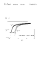
- Parasitic leakage paths are generally created due to the proximity of a semiconductor device to the sharp corners of a trench. The effect is reflected in FIG. 1, which shows a silicon substrate 10 , trench isolation 12 , gate oxide layer 14 , and gate layer 16 .
- a parasitic leakage path is created across the length of a transistor along a sharp trench corner, e.g., corner 20 , due to an increased gate electric field near the corner 20 . Processing often furthers this problem by sharpening the trench corners and/or thinning the gate dielectric near the corners.
- the method of Chatterjee et al. involves formation, on a silicon substrate 21 , of nitride barrier regions 22 ; formation of oxide regions 23 by LOCOS (FIG. 1 b ); removal of the oxide regions 23 ; application of silicon dioxide to form spacers 24 around the nitride barrier regions 22 (FIG. 1 c ); etching of the spacers 24 ; and then etching of the trenches 24 for STI (FIG. 1 d ).
- This complex method is not suitable for most commercial applications, for which simple, cost-effective processes are desired.
- a similar method involving a complex LOCOS/STI combination is taught by U.S. Pat. No.
- the corners of the silicon of the active regions are desirably rounded by a single oxidation step.
- the extent of rounding that substantially reduces problems caused by a sharp corner will vary, depending primarily on the amount of gate wrap-around.
- the oxidation step of the invention advantageously provides a radius of curvature of about 30 to about 80 nm.
- the oxidation step is advantageously performed in an environment and for a time and temperature that results in formation of a silicon dioxide layer about 50 nm to about 150 nm thick on a blank silicon wafer (hereafter referred to as an equivalent oxide layer).
- the temperature for oxidation ranges from about 950° C. to about 1100° C., the lower end of this range being more useful with wet oxidation (i.e., water vapor present), and the higher end with dry oxidation.
- the oxidation temperature affects the time required to attain the selected equivalent oxide layer, and the extent of rounding depends largely on the temperature, as well as the thickness of the equivalent oxide layer and the thickness of the oxidation barrier region.
- the process of the invention involves the steps of forming a stress relief region 32 , e.g., a pad oxide, on a silicon substrate 30 , forming an oxidation barrier region 34 , e.g., silicon nitride, over the stress relief region 32 , providing an opening in the stress relief 32 and oxidation barrier 34 regions, providing a trench 36 in the silicon substrate 30 at the opening, depositing a dielectric material 38 , typically silicon dioxide, in the trench 36 , optionally planarizing the dielectric trench material 38 , and subsequently performing the oxidation step.
- a dielectric material is an electrically insulating material, i.e., a material having a resistivity of about 10 6 ohm-cm or greater.
- the oxidation barrier and stress relief regions are typically stripped, and a gate oxide 42 is formed over the active regions of the silicon substrate 30 .
- the rounding provided by the oxidation remains. The invention thereby reduces or eliminates sharp corners that contribute to leakage current and other detrimental corner effects.
- FIG. 1 reflect conventional shallow trench isolation processes.
- FIGS. 2A-2H show the steps in one embodiment of the invention.
- FIGS. 3-14 are scanning electron micrographs of trench structures made according to the process of the invention and of a comparison structure.
- FIG. 15 reflects a model for determining the facet size resulting from the oxidation step.
- FIG. 16 shows the relationship between transistor width and threshold voltage for transistors made with and without the oxidation step of the invention.
- FIG. 17 shows the relationship between gate voltage and drain current for transistors made with and without the oxidation step of the invention.
- a stress relief region 32 is formed on a silicon substrate 30 .
- the stress relief region 32 is typically silicon dioxide, and is known in the art as a pad oxide.
- the region 32 is typically formed as a layer by a standard technique known to one skilled in the art, e.g., thermal oxidation, and is used primarily to prevent defects that normally exist if an oxidation barrier region 34 such as silicon nitride is formed directly on the silicon substrate 30 .
- a stress relief region is not always required. It is possible for other materials to be deposited directly on the silicon substrate 30 . When formed from silicon dioxide, the stress relief region 32 is typically about 5 to about 30 nm thick.
- An oxidation barrier region 34 is formed above, and typically directly on, the stress relief region 32 .
- the oxidation barrier region 34 is typically silicon nitride, and is also typically formed as a layer by standard techniques known to one skilled in the art, e.g., chemical vapor deposition. When formed from silicon nitride, the region 34 is typically about 60 to about 250 nm thick.
- the oxidation barrier region 34 inhibits underlying silicon from oxidizing during subsequent treatments.
- an opening or gap is defined on the oxidation barrier region 34 , and the oxidation barrier region 34 and the stress relief region 32 are removed at the defined opening.
- the gap width will vary depending on the particular device, but will typically be about 0.1 to about 1000 ⁇ m wide, as measured at the top surface of the silicon substrate 30 . Gaps over 1000 ⁇ m wide are also possible. It is possible to selectively form the stress relief and oxidation barrier regions 32 , 34 on certain portions of the silicon substrate 30 , as opposed to forming the regions 32 , 34 as layers and then stripping certain areas of the layers.
- a trench 36 is etched in the silicon substrate 30 using a standard technique known to those skilled in the art.
- the trench is about 200 to about 1000 nm deep, as measured from the top surface of the silicon substrate 30 .
- the process of etching the trench 36 normally creates some damage, e.g., dislocations in the silicon lattice, along the trench walls, and to repair some of this damage, it is possible to oxidize the trench walls, forming what is known as a thermal liner (not shown).
- the thermal liner is provided, for example, by heating to a temperature of about 900 to about 1100° C., in an atmosphere of 100% oxygen (dry), for a time sufficient to achieve a liner thickness of about 20 to about 40 nm.
- silicon dioxide 38 is deposited, typically such that the trench 36 is filled, as reflected in FIG. 2 C. It is possible to deposit other dielectric materials in the trench 36 , but the trench material advantageously contains a silicon oxide.
- the silicon dioxide 38 is typically provided by chemical vapor deposition (CVD), or by other standard techniques known to those skilled in the art.
- a planarization step e.g., chemical-mechanical polishing or another standard technique, is typically performed when the trench 36 is filled with the silicon oxide 38 , in order to provide a planar surface.
- the oxidation barrier region 34 typically acts as a planarization stop. The planarization, which gives the trench material a relatively flat, uniform surface, is useful in allowing relatively uniform oxidation during the subsequent oxidation step. Desirable control of the process is thereby attained.
- FIG. 2D shows the trench profile after such planarization.
- an oxidation step is performed. As shown in FIG. 2E, the oxidation is performed such that the silicon corners are rounded at the area where the trench silicon dioxide 38 meets the pad oxide 32 . The oxygen diffuses through the trench silicon dioxide to reach the corners. Typically, the oxidation step will also oxidize silicon lying along the trench 36 , forming a layer similar to the thermal liner discussed above. For this reason, it is possible to omit the step of forming a thermal liner after forming the trench 36 . The oxidation step will also typically densify the trench silicon oxide 38 . The oxidation step is advantageously performed in an environment and for a time and temperature that provides an equivalent oxide layer about 50 nm to about 150 nm thick.
- An advantageous temperature range for the oxidation step is from about 950° C. to about 1100° C., the lower end of this range being more useful with wet oxidation, and the higher end with dry oxidation.
- Wet oxidation at about 950° C. is typically faster than dry oxidation at higher temperatures, but is capable of introducing ammonia defects into the active regions of the device.
- An atmosphere of 99% oxygen and 1% dichloroethylene has been found to be useful for the oxidation step, and other oxygen-containing atmospheres are also contemplated.
- FIG. 2F shows a close-up view of the transformation of such flat areas to a rounded corner having a radius of curvature, r, and an overall facet size, f.
- the radius of curvature, r is advantageously about 30 to about 80 nm
- the overall facet size, f is advantageously about 20 to about 80 nm.
- the extent of faceting and rounding depends in large part on the combination of oxidation temperature, equivalent oxide layer, and the thickness of the oxidation barrier region. For example, a thicker oxidation barrier region will typically impede growth of the silicon dioxide bird's beak under the region, and a longer time and/or higher temperature, i.e., a thicker equivalent oxide layer, will be required to obtain the desired rounding.
- a model for determining the facet size subsequent to the oxidation step is reflected in Example 1 below.
- a corner is considered to be rounded when at least 30% of the portion of the corner's boundary within the overall facet, f, matches, to within a few nanometers, the perimeter of a single circle with radius, r.
- the remaining portions of the oxidation barrier region 34 , and the stress relief region 32 are typically stripped, providing silicon active regions 40 isolated by trench silicon dioxide 38 , as reflected in FIG. 2 G.
- a gate oxide 42 is typically formed over the active regions in accordance with standard practice known to one skilled in the art.
- the rounding provided by the oxidation step remains, reducing the sharp corners that contribute to leakage current in devices subsequently formed.
- the rounded corners of the trenches provide, among other things, transistors that exhibit a higher threshold voltage and lower off-current than transistors for which no oxidation step is performed, as reflected in Example 2 below.
- Each sample was prepared as follows: On a silicon substrate, a silicon dioxide (pad oxide) region was formed by thermal oxidation. The pad oxide region had a thickness of 30 nm for each sample. A silicon nitride region, of the varying thicknesses shown below, was formed on the pad oxide region by chemical vapor deposition. A gap, of the widths shown in Table I, was etched into the pad oxide and silicon nitride regions by a conventional method. After the gap was etched, the trench was etched in the silicon substrate by a conventional method. The trench had a depth, measured from the top surface of the silicon substrate, of 300 nm for each sample.
- a thermal liner about 36 nm thick was formed by heating the article to 1000° C. for 15 minutes.
- the trench was then filled with silicon dioxide by high density plasma enhanced chemical vapor deposition to a height of about 600 nm above the top surface of the silicon nitride.
- Chemical-mechanical polishing was performed to planarize the trench silicon dioxide to the level of the top surface of the silicon nitride, which acted as a polishing stop.
- the oxidation step was then performed at the environments (wet or dry), temperatures, equivalent oxide layers, and times shown in Table I. Scanning electron micrographs (FIGS. 3-14) were then taken of the trench profiles (the temperature information printed on FIG. 14 is incorrect and should read 1100° C.).
- FIGS. 3, 4 , and 6 - 14 show various degrees of rounding provided by the invention.
- FIG. 5 shows the trench profile of a comparative example where the oxidation step was omitted. It is clear from FIG. 5 that the step of forming a thermal liner has a very minor effect on the silicon corner where the trench silicon oxide meets the pad oxide. In particular, it was found that formation of a thermal liner typically resulted in an initial facet of about 10 nm.
- a model was developed for the facet size (f of FIG. 2F) that develops from the oxidation step.
- the facet is proportional to d barrier , the thickness of the oxidation barrier region, and d oxid , which is a function of (1) the distance, d, that oxygen must diffuse from the surface of the trench oxide to the corner to be rounded and (2) the thermal budget (e.g., time and temperature) of the process.
- d oxid the distance, d, that oxygen must diffuse from the surface of the trench oxide to the corner to be rounded
- the thermal budget e.g., time and temperature
- Transistors were fabricated by conventional CMOS fabrication processes known to one skilled in the art. For both transistors made with and without the oxidation step of the invention, the following process steps were performed. On a silicon substrate, a silicon dioxide (pad oxide) region was formed by thermal oxidation. The pad oxide region had a thickness of 30 nm. A silicon nitride region having a thickness of about 117 nm was formed on the pad oxide region by chemical vapor deposition. A gap of about 10 ⁇ m or greater was etched into the pad oxide and silicon nitride regions by a conventional method. After the gap was etched, the trench was etched in the silicon substrate by a conventional method. The trench had a depth, measured from the top surface of the silicon substrate, of 300 nm.
- a thermal liner about 36 nm thick was formed by heating the article to 1000° C. for 15 minutes.
- the trench was then filled with silicon dioxide by high density plasma enhanced chemical vapor deposition to a height of about 600 nm above the top surface of the silicon nitride.
- Chemical-mechanical polishing was performed to planarize the trench silicon dioxide to the level of the top surface of the silicon nitride, which acted as a polishing stop. Where corner-rounding oxidation was desired, the oxidation step was performed at a temperature of 1100° C. for a time sufficient to form a 150 nm equivalent oxide.
- FIG. 16 is a plot of transistor width versus the n-junction threshold voltage (N ⁇ V t ) for transistors having a length of 5 ⁇ m.
- Transistors fabricated with the corner-rounding oxidation step of the invention exhibited no reverse narrow channel effect (also known in the art as narrow width effect, as discussed in Chatterjee et al., “A Shallow Trench Isolation using LOCOS Edge for Preventing Corner Effects for 0.25/0.18 ⁇ m CMOS Technologies and Beyond,” discussed above), even at small channel widths.
- Transistors made without the oxidation step clearly showed some reverse narrow channel effect at smaller widths (e.g., less than 1 ⁇ m).
- the corner rounding that takes place during the oxidation step eliminated corner effects that lead to the reverse narrow channel effect in small-width transistors.
- the transistors had a length of 5 ⁇ m and a width of 0.4 ⁇ m.
- the transistors for which the oxidation step was performed desirably exhibited a higher threshold voltage and lower off-current.
- V G is gate voltage
- I D is drain current
- V BG is back gate voltage.
Landscapes
- Element Separation (AREA)
- Local Oxidation Of Silicon (AREA)
Abstract
Description
| TABLE I | |||||||
| Nitride | Radius of | ||||||
| Figure | Equivalent | Thickness | Curvature | ||||
| Number | Environment | Temp. (° C.) | Oxide (nm) | Time | (nm) | (nm)* | Gap (μm) |
| 3 | Dry | 1100 | 150 | 55 | min | 110 | 60 | 2 |
| 4 | Dry | 1100 | 150 | 55 | min | 110 | 60 | 0.5 |
| 5 | No | No | No | No | 150 | ** | 0.5 |
| (comparative) | oxidation | | oxidation | oxidation |
| 6 | Wet | 950 | 150 | 35 | |
60 | *** | 0.5 |
| 7 | Dry | 1000 | 150 | 4 | hours | 70 | 35 | 0.5 |
| 8 | Dry | 1100 | 150 | 55 | |
80 | 70 | 0.5 |
| 9 | Dry | 1100 | 150 | 55 | min | 50 | 80 | 0.5 |
| 10 | Dry | 1100 | 150 | 55 | min | 90 | 60 | 0.5 |
| 11 | Dry | 1100 | 150 | 55 | min | 130 | 40 | 0.5 |
| 12 | Dry | 1100 | 150 | 55 | min | 190 | 35 | 0.5 |
| 13 | Dry | 1100 | 50 | 5 | min | 65 | 30 | 0.5 |
| 14 | Dry | 1100 | 100 | 25 | |
60 | 50 | 0.5 |
| *The values have an error of approximately ± 5 nm | ||||||||
| **No rounding | ||||||||
| ***Only faceting observed | ||||||||
Claims (36)
Priority Applications (3)
| Application Number | Priority Date | Filing Date | Title |
|---|---|---|---|
| US08/903,974 US6566224B1 (en) | 1997-07-31 | 1997-07-31 | Process for device fabrication |
| KR1019980030480A KR19990014255A (en) | 1997-07-31 | 1998-07-29 | Device manufacturing process |
| JP10216354A JPH1197523A (en) | 1997-07-31 | 1998-07-31 | Device fabrication process |
Applications Claiming Priority (1)
| Application Number | Priority Date | Filing Date | Title |
|---|---|---|---|
| US08/903,974 US6566224B1 (en) | 1997-07-31 | 1997-07-31 | Process for device fabrication |
Publications (1)
| Publication Number | Publication Date |
|---|---|
| US6566224B1 true US6566224B1 (en) | 2003-05-20 |
Family
ID=25418327
Family Applications (1)
| Application Number | Title | Priority Date | Filing Date |
|---|---|---|---|
| US08/903,974 Expired - Lifetime US6566224B1 (en) | 1997-07-31 | 1997-07-31 | Process for device fabrication |
Country Status (3)
| Country | Link |
|---|---|
| US (1) | US6566224B1 (en) |
| JP (1) | JPH1197523A (en) |
| KR (1) | KR19990014255A (en) |
Cited By (22)
| Publication number | Priority date | Publication date | Assignee | Title |
|---|---|---|---|---|
| US20020190345A1 (en) * | 1999-07-16 | 2002-12-19 | Mitsubishi Denki Kabushiki Kaisha | Semiconductor device having an improved isolation structure, and method of manufacturing the semiconductor device |
| WO2003043078A3 (en) * | 2001-11-13 | 2003-11-06 | Advanced Micro Devices Inc | Preferential corner rounding of trench structures using post-fill oxidation |
| US20040056315A1 (en) * | 2001-03-14 | 2004-03-25 | Mitsubishi Denki Kabushiki Kaisha | Semiconductor device and manufacturing method thereof |
| US20040082141A1 (en) * | 2002-10-29 | 2004-04-29 | Toshikazu Mizukoshi | Method of fabricating a semiconductor device having trenches |
| US20040207039A1 (en) * | 2001-06-29 | 2004-10-21 | Kabushiki Kaisha Toshiba | Semiconductor device and method of manufacturing a semiconductor device |
| US20040214404A1 (en) * | 2003-01-27 | 2004-10-28 | Taishi Kubota | Manufacturing method of semiconductor device and oxidization method of semiconductor substrate |
| US6825087B1 (en) | 1999-11-24 | 2004-11-30 | Fairchild Semiconductor Corporation | Hydrogen anneal for creating an enhanced trench for trench MOSFETS |
| US20050023576A1 (en) * | 2003-07-31 | 2005-02-03 | Wen-Chin Lee | Semiconductor structure having a strained region and a method of fabricating same |
| US20050070089A1 (en) * | 2003-09-29 | 2005-03-31 | Taikan Iinuma | Method for manufacturing a semiconductor device |
| US20050245029A1 (en) * | 2002-07-29 | 2005-11-03 | Jeong-Hyuk Choi | Methods of fabricating flash memory devices having a sloped trench isolation structure |
| US20050275063A1 (en) * | 2003-01-29 | 2005-12-15 | Renesas Technology Corp. | Semiconductor device |
| US7078296B2 (en) | 2002-01-16 | 2006-07-18 | Fairchild Semiconductor Corporation | Self-aligned trench MOSFETs and methods for making the same |
| US20060208336A1 (en) * | 2003-09-08 | 2006-09-21 | Wen-Chin Lee | Semiconductor structure having a strained region and a method of fabricating same |
| US20070148908A1 (en) * | 2005-12-28 | 2007-06-28 | Byun Dong I | Method of forming trench isolation layer of semiconductor device |
| US20080315352A1 (en) * | 2007-06-22 | 2008-12-25 | Lim Hyun-Ju | Method of manufacturing semiconductor device |
| US20110084354A1 (en) * | 2009-10-13 | 2011-04-14 | Mitsubishi Electric Corporation | Semiconductor device and method of manufacturing a semiconductor device |
| US20110220914A1 (en) * | 2010-03-10 | 2011-09-15 | Mitsubishi Electric Corporation | Power semiconductor device and method of manufacturing the same |
| US8466496B2 (en) | 2011-11-17 | 2013-06-18 | International Business Machines Corporation | Selective partial gate stack for improved device isolation |
| US8779469B2 (en) | 2011-10-20 | 2014-07-15 | International Business Machines Corporation | Post-gate shallow trench isolation structure formation |
| US9653343B1 (en) * | 2016-05-04 | 2017-05-16 | United Mociroelectronics Corp. | Method of manufacturing semiconductor device with shallow trench isolation (STI) having edge profile |
| CN107437525A (en) * | 2016-05-25 | 2017-12-05 | 世界先进积体电路股份有限公司 | Semiconductor device and method of forming the same |
| US20230335431A1 (en) * | 2022-04-19 | 2023-10-19 | Silergy Semiconductor Technology (Hangzhou) Ltd | Semiconductor device and method for manufacturing the same |
Families Citing this family (11)
| Publication number | Priority date | Publication date | Assignee | Title |
|---|---|---|---|---|
| JP4244456B2 (en) | 1999-08-04 | 2009-03-25 | 株式会社デンソー | Manufacturing method of semiconductor device, manufacturing method of insulated gate bipolar transistor, and insulated gate bipolar transistor |
| US6864532B2 (en) | 2000-01-14 | 2005-03-08 | Denso Corporation | Semiconductor device and method for manufacturing the same |
| ITMI20010039A1 (en) | 2000-01-14 | 2002-07-11 | Denso Corp | SEMICONDUCTOR DEVICE AND METHOD FOR MANUFACTURING ITSELF |
| JP4200626B2 (en) | 2000-02-28 | 2008-12-24 | 株式会社デンソー | Method for manufacturing insulated gate type power device |
| KR100376875B1 (en) * | 2000-06-30 | 2003-03-19 | 주식회사 하이닉스반도체 | Method for forming isolation layer in semiconductor device |
| KR100499625B1 (en) * | 2000-06-30 | 2005-07-07 | 주식회사 하이닉스반도체 | A method for forming a field oxide of a semiconductor device |
| KR100856300B1 (en) * | 2002-07-03 | 2008-09-03 | 주식회사 하이닉스반도체 | Manufacturing Method of Flash Memory Cells |
| JP4577680B2 (en) * | 2004-04-13 | 2010-11-10 | エルピーダメモリ株式会社 | Manufacturing method of semiconductor device |
| KR100671667B1 (en) | 2004-06-14 | 2007-01-18 | 주식회사 하이닉스반도체 | Device Separator Formation Method of Semiconductor Device |
| KR100629606B1 (en) * | 2004-12-31 | 2006-09-27 | 동부일렉트로닉스 주식회사 | Improvement of Gate Oxide Quality in High Voltage Device Regions |
| US11610899B2 (en) * | 2021-06-15 | 2023-03-21 | Nanya Technology Corporation | Memory cell, memory array and method for defining active area of memory cell |
Citations (6)
| Publication number | Priority date | Publication date | Assignee | Title |
|---|---|---|---|---|
| US5387540A (en) | 1993-09-30 | 1995-02-07 | Motorola Inc. | Method of forming trench isolation structure in an integrated circuit |
| US5433794A (en) | 1992-12-10 | 1995-07-18 | Micron Technology, Inc. | Spacers used to form isolation trenches with improved corners |
| US5468676A (en) | 1992-09-23 | 1995-11-21 | Texas Instruments Incorporated | Trench isolation structure and method for forming |
| US5521422A (en) | 1994-12-02 | 1996-05-28 | International Business Machines Corporation | Corner protected shallow trench isolation device |
| US5679599A (en) * | 1995-06-22 | 1997-10-21 | Advanced Micro Devices, Inc. | Isolation using self-aligned trench formation and conventional LOCOS |
| US5811346A (en) * | 1997-04-14 | 1998-09-22 | Vlsi Technology, Inc. | Silicon corner rounding in shallow trench isolation process |
-
1997
- 1997-07-31 US US08/903,974 patent/US6566224B1/en not_active Expired - Lifetime
-
1998
- 1998-07-29 KR KR1019980030480A patent/KR19990014255A/en not_active Ceased
- 1998-07-31 JP JP10216354A patent/JPH1197523A/en active Pending
Patent Citations (6)
| Publication number | Priority date | Publication date | Assignee | Title |
|---|---|---|---|---|
| US5468676A (en) | 1992-09-23 | 1995-11-21 | Texas Instruments Incorporated | Trench isolation structure and method for forming |
| US5433794A (en) | 1992-12-10 | 1995-07-18 | Micron Technology, Inc. | Spacers used to form isolation trenches with improved corners |
| US5387540A (en) | 1993-09-30 | 1995-02-07 | Motorola Inc. | Method of forming trench isolation structure in an integrated circuit |
| US5521422A (en) | 1994-12-02 | 1996-05-28 | International Business Machines Corporation | Corner protected shallow trench isolation device |
| US5679599A (en) * | 1995-06-22 | 1997-10-21 | Advanced Micro Devices, Inc. | Isolation using self-aligned trench formation and conventional LOCOS |
| US5811346A (en) * | 1997-04-14 | 1998-09-22 | Vlsi Technology, Inc. | Silicon corner rounding in shallow trench isolation process |
Non-Patent Citations (12)
| Title |
|---|
| "A Shallow Trench Isolation Study for 0.25/1.18 mum CMOS Technologies and Beyond", by Chatterjee, A. et al., IEEE Electron Devices Societyf1, 1996 Symposium on VLSI Technology, pp. 156-157, Honolulu (1996). |
| "A Shallow Trench Isolation Study for 0.25/1.18 μm CMOS Technologies and Beyond", by Chatterjee, A. et al., IEEE Electron Devices Societyf1, 1996 Symposium on VLSI Technology, pp. 156-157, Honolulu (1996). |
| "A Shallow Trench Isolation Using LOCOS Edge for Preventing Corner Effects for 0.25/0.18 mum CMOS Technologies and Beyond", by Chatterjee, A. et al., IEEE, IEDM, pp. 32.3.1-32.3.4 (1996). |
| "A Shallow Trench Isolation Using LOCOS Edge for Preventing Corner Effects for 0.25/0.18 μm CMOS Technologies and Beyond", by Chatterjee, A. et al., IEEE, IEDM, pp. 32.3.1-32.3.4 (1996). |
| "A Three-Dimensional MOSFET Gate-Induced Drain Leakage Effect in Narrow Deep Submicron Devices", by Geissler, S. et al., IEEE, IEDM, pp. 32.5.1-32.5.4 (1991). |
| "Corner-Rounded Shallow Trench Isolation Technology to Reduce the Stress-Induced Tunnel Oxide Leakage Current for Highly Reliable Flash Memories", by Watanabe, H. et al., IEEE, pp. 32.4.1-32.4.4 (1996). |
| "Impact of Shallow Trench Isolation on Reliability of Buried-and Surface-Channel sub-mum PFET", by Tonti, W. et al., IEEE, 1995 IEEE International Reliability Physics Proceedings, 33rd Annual, Las Vegas, Nevada (Apr. 4-6, 1995). |
| "Impact of Shallow Trench Isolation on Reliability of Buried-and Surface-Channel sub-μm PFET", by Tonti, W. et al., IEEE, 1995 IEEE International Reliability Physics Proceedings, 33rd Annual, Las Vegas, Nevada (Apr. 4-6, 1995). |
| A Novel 0.25mum Shallow Trench Isolation Technology, by Chen, C. et al., IEEE, pp. 32.5.1-32.5.4 (1996). |
| A Novel 0.25μm Shallow Trench Isolation Technology, by Chen, C. et al., IEEE, pp. 32.5.1-32.5.4 (1996). |
| F. Nouri, et al. "A fully-integrated Shallow Trench Isolation process for 0.18 mum and beyong-optimization, stress reduction and electrical performance", VLSI Technology. |
| F. Nouri, et al. "A fully-integrated Shallow Trench Isolation process for 0.18 μm and beyong—optimization, stress reduction and electrical performance", VLSI Technology. |
Cited By (38)
| Publication number | Priority date | Publication date | Assignee | Title |
|---|---|---|---|---|
| US20020190345A1 (en) * | 1999-07-16 | 2002-12-19 | Mitsubishi Denki Kabushiki Kaisha | Semiconductor device having an improved isolation structure, and method of manufacturing the semiconductor device |
| US6855615B2 (en) * | 1999-07-16 | 2005-02-15 | Renesas Technology Corp. | Method of manufacturing semiconductor device having an improved isolation structure |
| US6825087B1 (en) | 1999-11-24 | 2004-11-30 | Fairchild Semiconductor Corporation | Hydrogen anneal for creating an enhanced trench for trench MOSFETS |
| US20040056315A1 (en) * | 2001-03-14 | 2004-03-25 | Mitsubishi Denki Kabushiki Kaisha | Semiconductor device and manufacturing method thereof |
| US20060244098A1 (en) * | 2001-06-29 | 2006-11-02 | Kabushiki Kaisha Toshiba | Semiconductor device and method of manufacturing a semiconductor device |
| US20040207039A1 (en) * | 2001-06-29 | 2004-10-21 | Kabushiki Kaisha Toshiba | Semiconductor device and method of manufacturing a semiconductor device |
| US7095093B2 (en) | 2001-06-29 | 2006-08-22 | Kabushiki Kaisha Toshiba | Semiconductor device and method of manufacturing a semiconductor device |
| WO2003043078A3 (en) * | 2001-11-13 | 2003-11-06 | Advanced Micro Devices Inc | Preferential corner rounding of trench structures using post-fill oxidation |
| US7078296B2 (en) | 2002-01-16 | 2006-07-18 | Fairchild Semiconductor Corporation | Self-aligned trench MOSFETs and methods for making the same |
| US20050245029A1 (en) * | 2002-07-29 | 2005-11-03 | Jeong-Hyuk Choi | Methods of fabricating flash memory devices having a sloped trench isolation structure |
| US7494868B2 (en) * | 2002-07-29 | 2009-02-24 | Samsung Electronics Co., Ltd. | Methods of fabricating flash memory devices having a sloped trench isolation structure |
| US20040082141A1 (en) * | 2002-10-29 | 2004-04-29 | Toshikazu Mizukoshi | Method of fabricating a semiconductor device having trenches |
| US20040214404A1 (en) * | 2003-01-27 | 2004-10-28 | Taishi Kubota | Manufacturing method of semiconductor device and oxidization method of semiconductor substrate |
| US7163871B2 (en) * | 2003-01-27 | 2007-01-16 | Elpida Memory, Inc. | Manufacturing method of semiconductor device and oxidization method of semiconductor substrate |
| US7355242B2 (en) | 2003-01-29 | 2008-04-08 | Renesas Technology Corp. | Semiconductor device |
| US20050275063A1 (en) * | 2003-01-29 | 2005-12-15 | Renesas Technology Corp. | Semiconductor device |
| US7115940B2 (en) | 2003-01-29 | 2006-10-03 | Renesas Technology Corp. | Semiconductor device |
| US20070023819A1 (en) * | 2003-01-29 | 2007-02-01 | Renesas Technology Corp. | Semiconductor device |
| US7045836B2 (en) * | 2003-07-31 | 2006-05-16 | Taiwan Semiconductor Manufacturing Company, Ltd. | Semiconductor structure having a strained region and a method of fabricating same |
| US20050023576A1 (en) * | 2003-07-31 | 2005-02-03 | Wen-Chin Lee | Semiconductor structure having a strained region and a method of fabricating same |
| US7495267B2 (en) * | 2003-09-08 | 2009-02-24 | Taiwan Semiconductor Manufacturing Company, Ltd. | Semiconductor structure having a strained region and a method of fabricating same |
| US20060208336A1 (en) * | 2003-09-08 | 2006-09-21 | Wen-Chin Lee | Semiconductor structure having a strained region and a method of fabricating same |
| US20050070089A1 (en) * | 2003-09-29 | 2005-03-31 | Taikan Iinuma | Method for manufacturing a semiconductor device |
| US7022584B2 (en) * | 2003-09-29 | 2006-04-04 | Oki Electric Industry Co., Ltd. | Method of manufacturing a shallow trench isolation structure |
| US20070148908A1 (en) * | 2005-12-28 | 2007-06-28 | Byun Dong I | Method of forming trench isolation layer of semiconductor device |
| US20080315352A1 (en) * | 2007-06-22 | 2008-12-25 | Lim Hyun-Ju | Method of manufacturing semiconductor device |
| US7745304B2 (en) * | 2007-06-22 | 2010-06-29 | Dongbu Hitek Co., Ltd. | Method of manufacturing semiconductor device |
| US20110084354A1 (en) * | 2009-10-13 | 2011-04-14 | Mitsubishi Electric Corporation | Semiconductor device and method of manufacturing a semiconductor device |
| US9431479B2 (en) * | 2009-10-13 | 2016-08-30 | Mitsubishi Electric Corporation | High breakdown voltage semiconductor device having a resurf layer |
| US8450183B2 (en) | 2010-03-10 | 2013-05-28 | Mitsubishi Electric Corporation | Power semiconductor device and method of manufacturing the same |
| US20110220914A1 (en) * | 2010-03-10 | 2011-09-15 | Mitsubishi Electric Corporation | Power semiconductor device and method of manufacturing the same |
| US8779469B2 (en) | 2011-10-20 | 2014-07-15 | International Business Machines Corporation | Post-gate shallow trench isolation structure formation |
| US8785291B2 (en) | 2011-10-20 | 2014-07-22 | International Business Machines Corporation | Post-gate shallow trench isolation structure formation |
| US8466496B2 (en) | 2011-11-17 | 2013-06-18 | International Business Machines Corporation | Selective partial gate stack for improved device isolation |
| US9653343B1 (en) * | 2016-05-04 | 2017-05-16 | United Mociroelectronics Corp. | Method of manufacturing semiconductor device with shallow trench isolation (STI) having edge profile |
| CN107437525A (en) * | 2016-05-25 | 2017-12-05 | 世界先进积体电路股份有限公司 | Semiconductor device and method of forming the same |
| CN107437525B (en) * | 2016-05-25 | 2020-11-20 | 世界先进积体电路股份有限公司 | Semiconductor device and method of forming the same |
| US20230335431A1 (en) * | 2022-04-19 | 2023-10-19 | Silergy Semiconductor Technology (Hangzhou) Ltd | Semiconductor device and method for manufacturing the same |
Also Published As
| Publication number | Publication date |
|---|---|
| KR19990014255A (en) | 1999-02-25 |
| JPH1197523A (en) | 1999-04-09 |
Similar Documents
| Publication | Publication Date | Title |
|---|---|---|
| US6566224B1 (en) | Process for device fabrication | |
| KR100195208B1 (en) | Method of forming an element isolation region in a semiconductor device | |
| US5811347A (en) | Nitrogenated trench liner for improved shallow trench isolation | |
| US6174785B1 (en) | Method of forming trench isolation region for semiconductor device | |
| US6265282B1 (en) | Process for making an isolation structure | |
| US5492858A (en) | Shallow trench isolation process for high aspect ratio trenches | |
| US6875649B2 (en) | Methods for manufacturing integrated circuit devices including an isolation region defining an active region area | |
| EP1213757B1 (en) | Integrated circuits having adjacent p-type doped regions having shallow trench isolation structures without liner layers therebetween and methods of forming same | |
| US7915173B2 (en) | Shallow trench isolation structure having reduced dislocation density | |
| US8173517B2 (en) | Method for forming a self-aligned isolation structure utilizing sidewall spacers as an etch mask and remaining as a portion of the isolation structure | |
| US6194283B1 (en) | High density trench fill due to new spacer fill method including isotropically etching silicon nitride spacers | |
| US6153480A (en) | Advanced trench sidewall oxide for shallow trench technology | |
| US20010041421A1 (en) | Trench isolatoin regions having trench liners with recessed ends | |
| KR930011458B1 (en) | Field oxide film formation method of semiconductor device | |
| US6093619A (en) | Method to form trench-free buried contact in process with STI technology | |
| US6331472B1 (en) | Method for forming shallow trench isolation | |
| US20030027402A1 (en) | Method for reducing stress of sidewall oxide layer of shallow trench isolation | |
| JPH1174508A (en) | Semiconductor device and manufacturing method thereof | |
| US6358818B1 (en) | Method for forming trench isolation regions | |
| KR100419689B1 (en) | Method for forming a liner in a trench | |
| US6221733B1 (en) | Reduction of mechanical stress in shallow trench isolation process | |
| US6358785B1 (en) | Method for forming shallow trench isolation structures | |
| KR100311708B1 (en) | Semiconductor device having a shallow isolation trench | |
| US6893940B2 (en) | Method of manufacturing semiconductor device | |
| US6794269B1 (en) | Method for and structure formed from fabricating a relatively deep isolation structure |
Legal Events
| Date | Code | Title | Description |
|---|---|---|---|
| AS | Assignment |
Owner name: LUCENT TECHNOLOGIES INC., NEW JERSEY Free format text: ASSIGNMENT OF ASSIGNORS INTEREST;ASSIGNORS:CHANG, CHORNG-PING;PAI, CHIEN-SHING;REEL/FRAME:008900/0067;SIGNING DATES FROM 19971013 TO 19971105 |
|
| STCF | Information on status: patent grant |
Free format text: PATENTED CASE |
|
| FPAY | Fee payment |
Year of fee payment: 4 |
|
| AS | Assignment |
Owner name: AGERE SYSTEMS INC., PENNSYLVANIA Free format text: ASSIGNMENT OF ASSIGNORS INTEREST;ASSIGNOR:LUCENT TECHNOLOGIES INC.;REEL/FRAME:018826/0855 Effective date: 20010130 |
|
| FPAY | Fee payment |
Year of fee payment: 8 |
|
| AS | Assignment |
Owner name: DEUTSCHE BANK AG NEW YORK BRANCH, AS COLLATERAL AG Free format text: PATENT SECURITY AGREEMENT;ASSIGNORS:LSI CORPORATION;AGERE SYSTEMS LLC;REEL/FRAME:032856/0031 Effective date: 20140506 Owner name: DEUTSCHE BANK AG NEW YORK BRANCH, AS COLLATERAL AGENT, NEW YORK Free format text: PATENT SECURITY AGREEMENT;ASSIGNORS:LSI CORPORATION;AGERE SYSTEMS LLC;REEL/FRAME:032856/0031 Effective date: 20140506 |
|
| FPAY | Fee payment |
Year of fee payment: 12 |
|
| AS | Assignment |
Owner name: AVAGO TECHNOLOGIES GENERAL IP (SINGAPORE) PTE. LTD., SINGAPORE Free format text: ASSIGNMENT OF ASSIGNORS INTEREST;ASSIGNOR:AGERE SYSTEMS LLC;REEL/FRAME:035365/0634 Effective date: 20140804 Owner name: AVAGO TECHNOLOGIES GENERAL IP (SINGAPORE) PTE. LTD Free format text: ASSIGNMENT OF ASSIGNORS INTEREST;ASSIGNOR:AGERE SYSTEMS LLC;REEL/FRAME:035365/0634 Effective date: 20140804 |
|
| AS | Assignment |
Owner name: AGERE SYSTEMS LLC, PENNSYLVANIA Free format text: TERMINATION AND RELEASE OF SECURITY INTEREST IN PATENT RIGHTS (RELEASES RF 032856-0031);ASSIGNOR:DEUTSCHE BANK AG NEW YORK BRANCH, AS COLLATERAL AGENT;REEL/FRAME:037684/0039 Effective date: 20160201 Owner name: LSI CORPORATION, CALIFORNIA Free format text: TERMINATION AND RELEASE OF SECURITY INTEREST IN PATENT RIGHTS (RELEASES RF 032856-0031);ASSIGNOR:DEUTSCHE BANK AG NEW YORK BRANCH, AS COLLATERAL AGENT;REEL/FRAME:037684/0039 Effective date: 20160201 |
|
| AS | Assignment |
Owner name: BANK OF AMERICA, N.A., AS COLLATERAL AGENT, NORTH CAROLINA Free format text: PATENT SECURITY AGREEMENT;ASSIGNOR:AVAGO TECHNOLOGIES GENERAL IP (SINGAPORE) PTE. LTD.;REEL/FRAME:037808/0001 Effective date: 20160201 Owner name: BANK OF AMERICA, N.A., AS COLLATERAL AGENT, NORTH Free format text: PATENT SECURITY AGREEMENT;ASSIGNOR:AVAGO TECHNOLOGIES GENERAL IP (SINGAPORE) PTE. LTD.;REEL/FRAME:037808/0001 Effective date: 20160201 |
|
| AS | Assignment |
Owner name: AVAGO TECHNOLOGIES GENERAL IP (SINGAPORE) PTE. LTD., SINGAPORE Free format text: TERMINATION AND RELEASE OF SECURITY INTEREST IN PATENTS;ASSIGNOR:BANK OF AMERICA, N.A., AS COLLATERAL AGENT;REEL/FRAME:041710/0001 Effective date: 20170119 Owner name: AVAGO TECHNOLOGIES GENERAL IP (SINGAPORE) PTE. LTD Free format text: TERMINATION AND RELEASE OF SECURITY INTEREST IN PATENTS;ASSIGNOR:BANK OF AMERICA, N.A., AS COLLATERAL AGENT;REEL/FRAME:041710/0001 Effective date: 20170119 |
|
| AS | Assignment |
Owner name: BELL SEMICONDUCTOR, LLC, ILLINOIS Free format text: ASSIGNMENT OF ASSIGNORS INTEREST;ASSIGNORS:AVAGO TECHNOLOGIES GENERAL IP (SINGAPORE) PTE. LTD.;BROADCOM CORPORATION;REEL/FRAME:044886/0001 Effective date: 20171208 |
|
| AS | Assignment |
Owner name: CORTLAND CAPITAL MARKET SERVICES LLC, AS COLLATERAL AGENT, ILLINOIS Free format text: SECURITY INTEREST;ASSIGNORS:HILCO PATENT ACQUISITION 56, LLC;BELL SEMICONDUCTOR, LLC;BELL NORTHERN RESEARCH, LLC;REEL/FRAME:045216/0020 Effective date: 20180124 Owner name: CORTLAND CAPITAL MARKET SERVICES LLC, AS COLLATERA Free format text: SECURITY INTEREST;ASSIGNORS:HILCO PATENT ACQUISITION 56, LLC;BELL SEMICONDUCTOR, LLC;BELL NORTHERN RESEARCH, LLC;REEL/FRAME:045216/0020 Effective date: 20180124 |
|
| AS | Assignment |
Owner name: BELL NORTHERN RESEARCH, LLC, ILLINOIS Free format text: SECURITY INTEREST;ASSIGNOR:CORTLAND CAPITAL MARKET SERVICES LLC;REEL/FRAME:060885/0001 Effective date: 20220401 Owner name: BELL SEMICONDUCTOR, LLC, ILLINOIS Free format text: SECURITY INTEREST;ASSIGNOR:CORTLAND CAPITAL MARKET SERVICES LLC;REEL/FRAME:060885/0001 Effective date: 20220401 Owner name: HILCO PATENT ACQUISITION 56, LLC, ILLINOIS Free format text: SECURITY INTEREST;ASSIGNOR:CORTLAND CAPITAL MARKET SERVICES LLC;REEL/FRAME:060885/0001 Effective date: 20220401 |