US6521386B1 - Electrophotographic photoreceptor and electrophotographic image forming method and apparatus using the photoreceptor - Google Patents
Electrophotographic photoreceptor and electrophotographic image forming method and apparatus using the photoreceptor Download PDFInfo
- Publication number
- US6521386B1 US6521386B1 US09/504,799 US50479900A US6521386B1 US 6521386 B1 US6521386 B1 US 6521386B1 US 50479900 A US50479900 A US 50479900A US 6521386 B1 US6521386 B1 US 6521386B1
- Authority
- US
- United States
- Prior art keywords
- charge carrier
- photoreceptor
- carrier transport
- transport layer
- layer
- Prior art date
- Legal status (The legal status is an assumption and is not a legal conclusion. Google has not performed a legal analysis and makes no representation as to the accuracy of the status listed.)
- Expired - Fee Related
Links
Images


Classifications
-
- G—PHYSICS
- G03—PHOTOGRAPHY; CINEMATOGRAPHY; ANALOGOUS TECHNIQUES USING WAVES OTHER THAN OPTICAL WAVES; ELECTROGRAPHY; HOLOGRAPHY
- G03G—ELECTROGRAPHY; ELECTROPHOTOGRAPHY; MAGNETOGRAPHY
- G03G5/00—Recording members for original recording by exposure, e.g. to light, to heat, to electrons; Manufacture thereof; Selection of materials therefor
- G03G5/02—Charge-receiving layers
- G03G5/04—Photoconductive layers; Charge-generation layers or charge-transporting layers; Additives therefor; Binders therefor
- G03G5/06—Photoconductive layers; Charge-generation layers or charge-transporting layers; Additives therefor; Binders therefor characterised by the photoconductive material being organic
- G03G5/0664—Dyes
- G03G5/0666—Dyes containing a methine or polymethine group
- G03G5/0668—Dyes containing a methine or polymethine group containing only one methine or polymethine group
-
- G—PHYSICS
- G03—PHOTOGRAPHY; CINEMATOGRAPHY; ANALOGOUS TECHNIQUES USING WAVES OTHER THAN OPTICAL WAVES; ELECTROGRAPHY; HOLOGRAPHY
- G03G—ELECTROGRAPHY; ELECTROPHOTOGRAPHY; MAGNETOGRAPHY
- G03G5/00—Recording members for original recording by exposure, e.g. to light, to heat, to electrons; Manufacture thereof; Selection of materials therefor
- G03G5/02—Charge-receiving layers
- G03G5/04—Photoconductive layers; Charge-generation layers or charge-transporting layers; Additives therefor; Binders therefor
- G03G5/043—Photoconductive layers characterised by having two or more layers or characterised by their composite structure
- G03G5/047—Photoconductive layers characterised by having two or more layers or characterised by their composite structure characterised by the charge-generation layers or charge transport layers
-
- G—PHYSICS
- G03—PHOTOGRAPHY; CINEMATOGRAPHY; ANALOGOUS TECHNIQUES USING WAVES OTHER THAN OPTICAL WAVES; ELECTROGRAPHY; HOLOGRAPHY
- G03G—ELECTROGRAPHY; ELECTROPHOTOGRAPHY; MAGNETOGRAPHY
- G03G5/00—Recording members for original recording by exposure, e.g. to light, to heat, to electrons; Manufacture thereof; Selection of materials therefor
- G03G5/02—Charge-receiving layers
- G03G5/04—Photoconductive layers; Charge-generation layers or charge-transporting layers; Additives therefor; Binders therefor
- G03G5/05—Organic bonding materials; Methods for coating a substrate with a photoconductive layer; Inert supplements for use in photoconductive layers
- G03G5/0503—Inert supplements
- G03G5/051—Organic non-macromolecular compounds
- G03G5/0514—Organic non-macromolecular compounds not comprising cyclic groups
-
- G—PHYSICS
- G03—PHOTOGRAPHY; CINEMATOGRAPHY; ANALOGOUS TECHNIQUES USING WAVES OTHER THAN OPTICAL WAVES; ELECTROGRAPHY; HOLOGRAPHY
- G03G—ELECTROGRAPHY; ELECTROPHOTOGRAPHY; MAGNETOGRAPHY
- G03G5/00—Recording members for original recording by exposure, e.g. to light, to heat, to electrons; Manufacture thereof; Selection of materials therefor
- G03G5/02—Charge-receiving layers
- G03G5/04—Photoconductive layers; Charge-generation layers or charge-transporting layers; Additives therefor; Binders therefor
- G03G5/05—Organic bonding materials; Methods for coating a substrate with a photoconductive layer; Inert supplements for use in photoconductive layers
- G03G5/0503—Inert supplements
- G03G5/051—Organic non-macromolecular compounds
- G03G5/0517—Organic non-macromolecular compounds comprising one or more cyclic groups consisting of carbon-atoms only
-
- G—PHYSICS
- G03—PHOTOGRAPHY; CINEMATOGRAPHY; ANALOGOUS TECHNIQUES USING WAVES OTHER THAN OPTICAL WAVES; ELECTROGRAPHY; HOLOGRAPHY
- G03G—ELECTROGRAPHY; ELECTROPHOTOGRAPHY; MAGNETOGRAPHY
- G03G5/00—Recording members for original recording by exposure, e.g. to light, to heat, to electrons; Manufacture thereof; Selection of materials therefor
- G03G5/02—Charge-receiving layers
- G03G5/04—Photoconductive layers; Charge-generation layers or charge-transporting layers; Additives therefor; Binders therefor
- G03G5/05—Organic bonding materials; Methods for coating a substrate with a photoconductive layer; Inert supplements for use in photoconductive layers
- G03G5/0503—Inert supplements
- G03G5/051—Organic non-macromolecular compounds
- G03G5/0521—Organic non-macromolecular compounds comprising one or more heterocyclic groups
-
- G—PHYSICS
- G03—PHOTOGRAPHY; CINEMATOGRAPHY; ANALOGOUS TECHNIQUES USING WAVES OTHER THAN OPTICAL WAVES; ELECTROGRAPHY; HOLOGRAPHY
- G03G—ELECTROGRAPHY; ELECTROPHOTOGRAPHY; MAGNETOGRAPHY
- G03G5/00—Recording members for original recording by exposure, e.g. to light, to heat, to electrons; Manufacture thereof; Selection of materials therefor
- G03G5/02—Charge-receiving layers
- G03G5/04—Photoconductive layers; Charge-generation layers or charge-transporting layers; Additives therefor; Binders therefor
- G03G5/05—Organic bonding materials; Methods for coating a substrate with a photoconductive layer; Inert supplements for use in photoconductive layers
- G03G5/0528—Macromolecular bonding materials
- G03G5/0557—Macromolecular bonding materials obtained otherwise than by reactions only involving carbon-to-carbon unsatured bonds
- G03G5/0564—Polycarbonates
-
- G—PHYSICS
- G03—PHOTOGRAPHY; CINEMATOGRAPHY; ANALOGOUS TECHNIQUES USING WAVES OTHER THAN OPTICAL WAVES; ELECTROGRAPHY; HOLOGRAPHY
- G03G—ELECTROGRAPHY; ELECTROPHOTOGRAPHY; MAGNETOGRAPHY
- G03G5/00—Recording members for original recording by exposure, e.g. to light, to heat, to electrons; Manufacture thereof; Selection of materials therefor
- G03G5/02—Charge-receiving layers
- G03G5/04—Photoconductive layers; Charge-generation layers or charge-transporting layers; Additives therefor; Binders therefor
- G03G5/06—Photoconductive layers; Charge-generation layers or charge-transporting layers; Additives therefor; Binders therefor characterised by the photoconductive material being organic
- G03G5/0601—Acyclic or carbocyclic compounds
- G03G5/0603—Acyclic or carbocyclic compounds containing halogens
-
- G—PHYSICS
- G03—PHOTOGRAPHY; CINEMATOGRAPHY; ANALOGOUS TECHNIQUES USING WAVES OTHER THAN OPTICAL WAVES; ELECTROGRAPHY; HOLOGRAPHY
- G03G—ELECTROGRAPHY; ELECTROPHOTOGRAPHY; MAGNETOGRAPHY
- G03G5/00—Recording members for original recording by exposure, e.g. to light, to heat, to electrons; Manufacture thereof; Selection of materials therefor
- G03G5/02—Charge-receiving layers
- G03G5/04—Photoconductive layers; Charge-generation layers or charge-transporting layers; Additives therefor; Binders therefor
- G03G5/06—Photoconductive layers; Charge-generation layers or charge-transporting layers; Additives therefor; Binders therefor characterised by the photoconductive material being organic
- G03G5/0601—Acyclic or carbocyclic compounds
- G03G5/0605—Carbocyclic compounds
- G03G5/0607—Carbocyclic compounds containing at least one non-six-membered ring
-
- G—PHYSICS
- G03—PHOTOGRAPHY; CINEMATOGRAPHY; ANALOGOUS TECHNIQUES USING WAVES OTHER THAN OPTICAL WAVES; ELECTROGRAPHY; HOLOGRAPHY
- G03G—ELECTROGRAPHY; ELECTROPHOTOGRAPHY; MAGNETOGRAPHY
- G03G5/00—Recording members for original recording by exposure, e.g. to light, to heat, to electrons; Manufacture thereof; Selection of materials therefor
- G03G5/02—Charge-receiving layers
- G03G5/04—Photoconductive layers; Charge-generation layers or charge-transporting layers; Additives therefor; Binders therefor
- G03G5/06—Photoconductive layers; Charge-generation layers or charge-transporting layers; Additives therefor; Binders therefor characterised by the photoconductive material being organic
- G03G5/0601—Acyclic or carbocyclic compounds
- G03G5/0609—Acyclic or carbocyclic compounds containing oxygen
-
- G—PHYSICS
- G03—PHOTOGRAPHY; CINEMATOGRAPHY; ANALOGOUS TECHNIQUES USING WAVES OTHER THAN OPTICAL WAVES; ELECTROGRAPHY; HOLOGRAPHY
- G03G—ELECTROGRAPHY; ELECTROPHOTOGRAPHY; MAGNETOGRAPHY
- G03G5/00—Recording members for original recording by exposure, e.g. to light, to heat, to electrons; Manufacture thereof; Selection of materials therefor
- G03G5/02—Charge-receiving layers
- G03G5/04—Photoconductive layers; Charge-generation layers or charge-transporting layers; Additives therefor; Binders therefor
- G03G5/06—Photoconductive layers; Charge-generation layers or charge-transporting layers; Additives therefor; Binders therefor characterised by the photoconductive material being organic
- G03G5/0601—Acyclic or carbocyclic compounds
- G03G5/0612—Acyclic or carbocyclic compounds containing nitrogen
- G03G5/0614—Amines
- G03G5/06142—Amines arylamine
- G03G5/06147—Amines arylamine alkenylarylamine
-
- G—PHYSICS
- G03—PHOTOGRAPHY; CINEMATOGRAPHY; ANALOGOUS TECHNIQUES USING WAVES OTHER THAN OPTICAL WAVES; ELECTROGRAPHY; HOLOGRAPHY
- G03G—ELECTROGRAPHY; ELECTROPHOTOGRAPHY; MAGNETOGRAPHY
- G03G5/00—Recording members for original recording by exposure, e.g. to light, to heat, to electrons; Manufacture thereof; Selection of materials therefor
- G03G5/02—Charge-receiving layers
- G03G5/04—Photoconductive layers; Charge-generation layers or charge-transporting layers; Additives therefor; Binders therefor
- G03G5/06—Photoconductive layers; Charge-generation layers or charge-transporting layers; Additives therefor; Binders therefor characterised by the photoconductive material being organic
- G03G5/07—Polymeric photoconductive materials
- G03G5/075—Polymeric photoconductive materials obtained otherwise than by reactions only involving carbon-to-carbon unsaturated bonds
Definitions
- the present invention relates to an electrophotographic photoreceptor, and to an electrophotographic image forming method and apparatus using the photoreceptor.
- Electrophotographic image forming methods such as Carlson process and modified process thereof have been widely used for image forming apparatus such as copiers and printers.
- image forming apparatus such as copiers and printers.
- organic photoreceptors are widely used because of being low-priced and pollution-free, and having good productivity.
- Organic photoreceptors are broadly classified into photoconductive resin type photoreceptors including a photoconductive resin such as polyvinylcarbazole (PVK); charge-transfer complex type photoreceptors including, for example, PVK-TNF (2,4,7-trinitrofluorenone); pigment-dispersed type photoreceptors in which a pigment such as phthalocyanine pigments is dispersed in a resin; and functionally-separated photoreceptors including a combination of a charge carrier generation material and a charge carrier transport material.
- PVK polyvinylcarbazole
- charge-transfer complex type photoreceptors including, for example, PVK-TNF (2,4,7-trinitrofluorenone
- pigment-dispersed type photoreceptors in which a pigment such as phthalocyanine pigments is dispersed in a resin
- functionally-separated photoreceptors including a combination of a charge carrier generation material and a charge carrier transport material.
- the mechanism of formation of electrostatic latent images on a typical functionally-separated organic photoreceptor having a photoreceptive layer including a charge carrier generation layer and a charge carrier transport layer are as follows:
- the injected charge carriers are transported through the charge carrier transport layer by an electric field caused by the charging of the photoreceptor, and finally neutralize the charge formed on the surface of the photoreceptor, resulting in formation of an electrostatic latent image on the photoreceptor.
- Organic photoreceptors preferably have the following properties:
- Japanese Laid-Open Patent Publications Nos. 8-6450 and 8-62862 have disclosed photoreceptors useful for high speed image recording, which include an organic charge carrier transport material having a charge mobility in a specified range.
- an organic charge carrier transport material having a charge mobility in a specified range.
- a problem in which resolution of the resultant images deteriorates or the resultant photoreceptor does not have high photoresponse tends to occur.
- Japanese Laid-Open Patent Publications Nos. 4-287052 and 5-165384 have disclose photoreceptors which include a component capable of decreasing the friction coefficient of the photoreceptors.
- Japanese Laid-Open Patent Publications Nos. 6-342236 and 9-81001 have disclose image forming apparatus in which a device applying a component, which decreases the friction coefficient of the photoreceptor thereof, is provided.
- these techniques have not been applied to a photoreceptor used for high speed recording.
- Japanese Laid-Open Patent Publication No. 8-272198 discloses an image forming apparatus in which the charge mobility of the photoreceptive layer, the thickness of the photoreceptive layer, the moving speed of the image bearing member configured to face the photoreceptor, and the electric field formed in the photoreceptive layer are set at proper values so as to satisfy a specific relationship to avoid formation of tailing of images.
- the image forming apparatus having such a structure cannot perform high speed recording.
- an object of the present invention is to provide a photoreceptor which can exhibit an excellent combination of high photoresponse and good durability so as to be used for high speed image forming apparatus.
- Another object of the present invention is to provide an image forming method and apparatus which can produce good images at a high speed even upon use of a photoreceptor for a long period of time.
- an electrophotographic photoreceptor including an electroconductive substrate and a photoreceptive layer, which is formed overlying the substrate, wherein the photoreceptive layer includes a charge carrier generation layer including a charge carrier generation material and a charge carrier transport layer including a charge carrier transport material, and wherein when an electric field of from 2.5 ⁇ 10 5 V/cm to 5.5 ⁇ 10 5 V/cm is applied to the charge carrier transport layer, the following relationship is satisfied:
- t CTL represents a thickness of the charge carrier transport layer and ⁇ CTL represents a charge mobility of the charge carrier transport layer.
- the charge carrier transport material preferably includes a high-molecular-weight charge carrier transport material.
- the surface of the photoreceptor preferably has a friction coefficient not greater than 0.5.
- Another aspect of the present invention is to provide an electrophotographic image forming method including the steps of charging the photoreceptor mentioned above, irradiating the charge photoreceptor with imagewise light to form an electrostatic latent image, and developing the latent image with a developer to form a visible image.
- Yet another aspect of the present invention is to provide an electrophotographic image forming apparatus (process cartridge) including at least the photoreceptor mentioned above, a charging device, an imagewise light irradiating device, a developing device, an image transferring device and an image fixing device.
- the apparatus preferably has a friction coefficient controlling device which controls a friction coefficient of a surface of the photoreceptor preferably by applying a lubricant to the surface of the photoreceptor
- FIG. 1 is a schematic view illustrating a cross section of an embodiment of the photoreceptor of the present invention
- FIG. 2 is a schematic view illustrating a cross section of another embodiment of the photoreceptor of the present invention.
- FIG. 3 is a schematic view illustrating an instrument useful for measuring friction coefficient of a photoreceptor according to an Euler method
- FIG. 4 is a schematic view illustrating an embodiment of the image forming process cartridge of the present invention.
- a photoreceptor having high photoresponse can be obtained by imparting to a charge carrier transport layer a property such that when an electric field of from 2.5 ⁇ 10 5 V/cm to 5.5 ⁇ 10 5 V/cm is applied to the charge carrier transport layer, the following relationship is satisfied in the charge carrier transport layer:
- t CTL represents a thickness of the charge carrier transport layer and ⁇ CTL represents a charge mobility of the charge carrier transport layer.
- the photoreceptor of the present invention has good surface potential decay properties even when a short-pulse light is radiated thereto to form an electrostatic latent image, and therefore can be satisfactorily used for high speed electrophotographic recording.
- the resultant photoreceptor has good resistance to abrasion (i.e., good durability).
- FIG. 1 is a schematic view illustrating a cross section of an embodiment of the photoreceptor of the present invention.
- a multi-layer photoreceptor is illustrated in which a charge carrier generation layer 17 is formed on an electroconductive substrate, and a charge carrier transport layer 19 is formed on the charge carrier generation layer 17 .
- a charge carrier transport layer 19 is formed on an electroconductive substrate 11 , and a charge carrier generation layer is formed on the charge carrier transport layer 19 .
- the combination of the charge carrier generation layer 17 and charge carrier transport layer 19 is hereinafter referred to as a photoreceptive layer.
- the thickness of the photoreceptive layer largely influences the resolution of the formed images.
- a negative-charge type multi-layer photoreceptor having the structure as shown in FIG. 1, positive and negative carriers are formed in the charge carrier generation layer 17 by irradiation of light.
- negative carriers i.e., electrons
- the positive carriers i.e., positive holes
- the electric field which causes the positive holes to move to the surface of the photoreceptor, decreases gradually. Therefore, the positive holes tend to move toward the portion of the photoreceptor which is not exposed to light. This phenomenon, which is referred to as diffusion of carriers toward the surface of the photoreceptor, causes the resolution of latent images to deteriorate. To thin the charge carrier transport layer 19 is effective for maintenance of good resolution.
- laser light is currently used for imagewise light irradiation.
- Laser light used for imagewise light irradiation has a photon flux of about 10 7 times that of the light radiated by a halogen lamp conventionally used for this use. Therefore, the density of carrier generated in the charge carrier generation layer extremely increases, and the electric field of the charge carrier transport layer is decreased by the carrier moved from the charge carrier generation layer.
- the moving speed of the carriers is influenced by the irradiation of laser light, and the carriers, which are generated in an area of the charge carrier generation layer to which the central part of the laser light spot is radiated, tend to reach late the surface of the photoreceptor.
- the thus formed space charges cause the carriers to diffuse into the horizontal direction of the photoreceptive layer (i.e., a direction parallel to the surface of the photoreceptor), resulting in deterioration of resolution of latent images.
- Suitable materials for use as the electroconductive substrate of the photoreceptor of the present invention includes a material having a volume resistivity less than 10 10 ⁇ m.
- Specific examples of such materials include drums and sheets which are made of plastics and paper and whose surfaces are coated with a metal such as aluminum, nickel, chrome, nickel-chrome alloys, copper, silver, gold, platinum and the like, or a metal oxide such as tin oxide and indium oxide, by a vacuum deposition method or a sputtering method.
- a plate of a metal such as aluminum, aluminum alloys, nickel, stainless steel and the like and a tube which is made, for example, by preparing a rough tube of a metal mentioned above by an extruding or a drawing method and then treating the surface of the rough tube by cutting, super finishing and/or polishing can also be used as a substrate.
- the charge carrier generation layer 17 includes a charge carrier generation material as a main component.
- Suitable charge carrier generation materials include organic materials such as monoazo pigments, disazo pigments, trisazo pigments, perylene type pigments, perynone type pigments, quinacridone type pigments, quinone type condensed polycyclic compounds, squaric acid type dyes, phthalocyanine type pigments, naphthalocyanine type pigments, and azulenium salt type dyes; and inorganic compounds such as selenium, selenium-tellurium selenium-arsenic alloys, and amorphous silicon.
- the charge carrier generation layer 17 can be formed by coating a coating liquid, which is prepared by dispersing or dissolving one or more charge carrier generation materials in a proper solvent, if desired, together with a binder resin, using a ball mill, an attritor, a sand mill or the like dispersing device, and then drying the coated liquid.
- a coating liquid which is prepared by dispersing or dissolving one or more charge carrier generation materials in a proper solvent, if desired, together with a binder resin, using a ball mill, an attritor, a sand mill or the like dispersing device, and then drying the coated liquid.
- Suitable coating methods include dip coating methods, spray coating methods, bead coating methods and the like coating methods.
- binder resins for use in the charge carrier generation layer 15 include polyamide resins, polyurethane resins, polyester resins, epoxy resins, polyketone resins, polycarbonate resins, silicone resins, acrylic resins, polyvinyl butyral resins, polyvinyl formal resins, polyvinyl ketone resins, polystyrene resins, polyacrylamide resins, and the like resins.
- Suitable solvents for use in the charge carrier generation layer coating liquid include tetrahydrofuran, cyclohexanone, dioxane, 2-butanone, dichloroethane, and the like solvents.
- the content of the binder resin in the charge carrier generation layer 17 is from 0 to 2 parts by weight per 1 part by weight of the charge carrier generation material included in the charge carrier generation layer 17 .
- the thickness of the charge carrier generation layer 17 is from 0.01 to 5 ⁇ m, and preferably from 0.1 to 2 ⁇ m.
- the charge carrier generation layer 17 can also be formed by any known vacuum film forming method.
- the charge carrier transport layer 19 can be formed by coating a coating liquid in which a charge carrier transport material and a binder resin are dissolved or dispersed in a proper solvent, and drying the coated liquid. Additives such as plasticizers, leveling agents and antioxidants can also be included in the coating liquid if desired.
- low-molecular-weight charge carrier transport materials are classified into positive-hole transporting materials and electron transporting materials.
- the electron transporting materials include electron accepting materials such as chloranil, bromanil, tetracyanoethylene, tetracyanoquinodimethane, 2,4,7-trinitro-9-fluorenone, 2,4,5,7-tetranitro-9-fluorenone, 2,4,5,7-tetranitroxanthone, 2,4,8-trinitrothioxanthone, 2,6,8-trinitro-indeno-4H-indeno[1,2-b]thiophene-4-one, 1,3,7-trinitrodibenzothiophene-5,5-dioxide, and the like.
- electron accepting materials such as chloranil, bromanil, tetracyanoethylene, tetracyanoquinodimethane, 2,4,7-trinitro-9-fluorenone, 2,4,5,7-tetranitro-9-fluorenone, 2,4,5,7-tetranitroxanthone, 2,4,8-trinitrothioxanthone, 2,6,8-trinitro-indeno-4H
- positive-hole transporting materials include electron donating materials such as oxazole derivatives, oxadiazole derivatives, imidazole derivatives, triphenyl amine derivatives, 9-(p-diethylaminostyrylanthracene, 1,1-bis-(4-dibenzylaminophenyl)propane, styryl anthracene, styryl pyrazoline, phenyl hydrazone compounds, a-phenyl stilbene derivatives, thiazole derivatives, phenazine derivatives, acridine derivatives, benzofuran derivatives, benzimidazole derivatives, thiophene derivatives and the like. These positive-hole transport materials are used alone or in combination.
- the charge carrier transport layer 19 can also be formed by coating a coating liquid, in which a high-molecular-weight charge carrier transport material is dissolved or dispersed in a proper solvent, and then drying the coated liquid.
- the high-molecular-weight charge carrier transport material includes known materials in which one or more of the charge transport substituents included in the low-molecular-weight charge carrier transport materials mentioned above are included in a main chain or a side chain of a high-molecular-weight material.
- the charge carrier transport layer of this type may include a binder resin, a low-molecular-weight charge carrier transport material, a plasticizer, a leveling agent, a lubricant and the like in a proper amount, if desired.
- binder resins for use in the charge carrier transport layer 19 include thermoplastic resins and thermosetting resins such as polystyrene resins, styrene-acrylonitrile copolymers, styrene-butadiene copolymers, styrene-maleic anhydride copolymers, polyester resins, polyvinyl chloride resins, vinyl chloride-vinyl acetate copolymers, polyvinyl acetate resins, polyvinylidene chloride resins, polyarylate resins, phenoxy resins, polycarbonate resins, cellulose acetate resins, ethyl cellulose resins, polyvinyl butyral resins, polyvinyl formal resins, polyvinyl toluene resins, acrylic resins, silicone resins, epoxy resins, melamine resins, urethane resins, phenolic resins, alkyd resins, and the like.
- thermoplastic resins and thermosetting resins such as polys
- solvent for use in the charge carrier transport layer coating liquid include tetrahydrofuran, dioxane, toluene, 2-butanone, monochlorobenzene, dichloroethane, methylene chloride, and the like solvents.
- the charge carrier transport layer 19 may includes a plasticizer and a leveling agent.
- plasticizer examples include known plasticizers, which are used as a plasticizer for general resins, such as dibutyl phthalate, dioctyl phthalate, and the like plasticizers.
- the addition amount of the plasticizer in the charge carrier transport layer 19 is 0 to 30% by weight of the binder resin used.
- the leveling agent examples include silicone oils such as dimethyl silicone oils and methyl phenyl silicone oils, and polymers and oligomers including a perfluoroalkyl group in their side chains.
- the addition amount of the leveling agent is from 0 to 1% by weight of the binder resin included in the charge carrier transport layer 19 .
- the thickness of the charge carrier transport layer 19 is preferably from 5 to 30 ⁇ m. The thickness is determined depending on the desired characteristics of the photoreceptor.
- the content of the charge carrier transport material in the charge carrier transport layer 19 is not less than 40% by weight.
- the charge formed on the resultant photoreceptor cannot sufficiently be decayed by exposure of pulsed light having a pulse width not greater than 5 ⁇ m. Namely the photoreceptor cannot be used for high speed electrophotographic image forming apparatuses.
- the charge carrier transport material is a high-molecular-weight charge carrier transport material
- the substituents having a charge transporting function are preferably included in the charge carrier transport layer in an amount of not less than 40% by weight.
- the charge mobility of the charge carrier transport layer 19 is preferably controlled so as to be not less than 3 ⁇ 10 ⁇ 5 cm 2 /V ⁇ s when an electric field of from 2.5 ⁇ 10 5 to 5.5 ⁇ 10 5 V/cm is applied to the charge carrier transport layer.
- the charge mobility can be obtained by a known TOF method. Namely, a film of a charge carrier transport layer of about 7.5 ⁇ m thick is formed on a polyester film having an aluminum electrode. Then a gold electrode of about 250 ⁇ thick is formed thereon to prepare a sample to be measured. Laser light is radiated from the aluminum electrode side using a nitrogen pulse laser as a light source, and the charge mobility is calculated by the transitional photo-current detected. The measurement is performed at room temperature (25° C.).
- the charge mobility of a charge carrier transport layer of a multi-layer photoreceptor consisting of a charge carrier generation layer and the charge carrier transport layer can be measured by a Xerographic Time of Flight method (XTOF).
- XTOF Xerographic Time of Flight method
- a photoreceptor to be measured is exposed to pulse light having a pulse width not greater than 5 ⁇ s in half width, which is radiated by a xenon flash lamp, while the surface potential of the photoreceptor is measured by a high speed surface potential meter (TREK 362A)
- the charge mobility can be determined by the surface potential decay curve soon after the light is radiated to the photoreceptor.
- the electrophotographic photoreceptor may include an undercoat layer between the electroconductive substrate 11 and a photoreceptive layer.
- the undercoat layer includes a resin as a main component. Suitable resins for use in the undercoat layer include resins which have good resistance to general organic solvents because the photoreceptive layer coating liquid is coated on the undercoat layer to form the photoreceptive layer thereon.
- resins include water-soluble resins such as polyvinyl alcohol, casein, polyacrylic acid sodium salt, and the like resins; alcohol-soluble resins such as nylon copolymers, methoxymethylated nylons and the like; and crosslinking resins, which can form a three-dimensional network structure, such as polyurethane resins, melamine resins, alkyd-melamine resins, epoxy resins and the like.
- the undercoat layer may include a particulate metal oxide such as titanium oxide, silica, aluminum oxide, zirconium oxide, tin oxide, indium oxide and the like to prevent occurrence of moiréin recorded images and to decrease the residual potential of the photoreceptor.
- the undercoat layer can be formed by a coating method similar to the method of forming the photoreceptive layer.
- a metal oxide layer which is formed by, for example, a sol-gel method using a silane coupling agent, a titanium coupling agent, a chromium coupling agent or the like, can also be used as the undercoat layer.
- an alumina layer which is formed by an anodic oxidation method and a layer which is formed by depositing an organic material such as polyparaxylylene or an inorganic material such as SiO, SnO 2, TiO 2 , ITO, CeO 2 , and the like by a vacuum thin film forming method can also be used as the undercoat layer.
- the thickness of the undercoat layer is preferably from 0 to 5 ⁇ m.
- a protective layer is formed on the photoreceptive layer to protect the photoreceptive layer.
- the materials for use in the protective layer include ABS resins, ACS resins, olefin-vinyl monomer copolymers, chlorinated polyether resins, aryl resins, phenolic resins, polyacetal resins, polyamide resins, polyamideimide resins, polyacrylate resins, polyarylsulfone resins, polybutylene resins, polybutyleneterephthalate resins, polycarbonate resins, polyethersulfone resins, polyethylene resins, polyethyleneterephthalate resins, polyimide resins, acrylic resins, polymethylpentene resins, polypropylene resins, polyphenylene oxide resins, polysulfone resins, As resins, AB resins, BS resins, polyurethane resins, polyvinyl chloride resins, polyvinylidene chloride resins, epoxy resins and the like.
- the protective layer may include a lubricating resin such as fluorine-containing resins like polytetrafluoroethylene and silicone resins to improve the abrasion resistance of the photoreceptor.
- a lubricating resin such as fluorine-containing resins like polytetrafluoroethylene and silicone resins to improve the abrasion resistance of the photoreceptor.
- an inorganic material such as titanium oxides, tin oxides, potassium titanate and the like may be dispersed in the lubricating resins.
- the protective layer can be formed by a general coating method.
- the thickness of the protective layer is preferably from 0.5 to 10 ⁇ m.
- the protective layer can be formed by depositing i-C, a-SiC and the like material by a vacuum thin film forming method.
- an intermediate layer may be formed between the photoreceptive layer and the protective layer.
- the intermediate layer includes a resin as a main component.
- the resin include polyamide resins, alcohol-soluble nylon resins, water-soluble polyvinyl butyral resins, polyvinyl butyral resins, polyvinyl alcohols, and the like resins.
- the intermediate layer can be formed by any one of the known coating methods mentioned above.
- the thickness of the intermediate layer is preferably from 0.05 to 2 ⁇ m.
- a lubricant is preferably included at least in a top layer, i.e., the farthest layer from the electroconductive substrate 11 , together with the charge carrier transport material to enhance the friction coefficient, water-repelling ability and releasability of the photoreceptor.
- the lubricant include fluorine-containing oils such as perfluoropolyether oils having a linear structure. The average molecular weight thereof is preferably from 2000 to 9000.
- the fluorine-containing oils are used alone or in combination.
- the content of the fluorine-containing oil in the top layer of the photoreceptor is preferably from 0.1 to 5% by weight to exert its effect and not to deteriorate good film formability of the top layer.
- silicone oils, metal soaps and fluorine-containing resins can also be used as a lubricant.
- the abrasion of the photoreceptor has to be controlled so as to be as small as possible.
- the electric properties of the photoreceptor such as charging properties, and surface potential decay properties caused by light irradiation change.
- the electric properties of the photoreceptor change good images cannot be obtained when the charging and imagewise light irradiation processes are performed under the predetermined conditions.
- the abrasion of the photoreceptor occurs at positions at which the photoreceptor contacts other members of the image forming apparatus.
- the cleaning unit which removes the toner particles remaining on the photoreceptor with a blade or a brush, abrades the photoreceptor more seriously than the other members.
- the abrasion of the photoreceptor caused by the cleaning unit is classified into two types.
- One of the types is abrasion caused by shear stress generated between the blade (or brush) and the photoreceptor.
- Another type is abrasion caused by the residual toner particles which are present between the photoreceptor and the blade (or brush) of the cleaning unit. The toner particles abrade the photoreceptor while serving like a grinding stone.
- the abrasion of the photoreceptor depends on the factors such as the mechanical strength of the photoreceptor, the contact pressure of the blade (or brush), the hardness of the toner particles and the friction coefficient ( ⁇ ) of the photoreceptor.
- factors such as the mechanical strength of the photoreceptor, the contact pressure of the blade (or brush), the hardness of the toner particles and the friction coefficient ( ⁇ ) of the photoreceptor.
- ⁇ the friction coefficient of the photoreceptor. Therefore, by controlling the friction coefficient of the surface of the photoreceptor so as to be relatively low, the abrasion of the photoreceptor can be improved.
- One of the methods of controlling the friction coefficient of the surface of the photoreceptor is to include a lubricant in the top layer as mentioned above.
- Another method of controlling the friction coefficient of the surface of the photoreceptor is to supply a lubricant material on the surface of the photoreceptor when the photoreceptor is used in an image forming apparatus.
- the lubricant material can be applied to the surface of the photoreceptor using a brush roller, an elastic roller, an elastic blade, a brush, a belt and the like member.
- Contact charging members in the image forming apparatus and transfer members can serve as the lubricant supplying member.
- Suitable materials for use as the lubricant, which is applied to the surface of the photoreceptor include liquid, solid or powdery lubricating materials.
- the lubricating material itself can serve as the lubricant supplying member.
- lubricating liquids such as silicone oils, fluorine-containing oils and the like oils
- lubricating solids and powders such as fluorine-containing resins, e.g., polytetrafluoroethylene (PTFE), perfluoroalkylvinyl ether (PFA) and polyvinylidene fluoride (PVDF), silicone resins, polyolefin resins, silicone greases, fluorine-containing greases, paraffin waxes, fatty acid metal salts such as zinc stearate, graphite, molybdenum disulfide and the like.
- fluorine-containing resins e.g., polytetrafluoroethylene (PTFE), perfluoroalkylvinyl ether (PFA) and polyvinylidene fluoride (PVDF)
- silicone resins e.g., polytetrafluoroethylene (PTFE), perfluoroalkylvinyl ether (PFA) and polyvinylid
- the friction coefficient of the surface of the photoreceptor is preferably controlled so as to be not greater than 0.5 when measured by an Euler belt method.
- the friction coefficient is too low, i.e., less than about 0.1 and typically less than about 0.05, good toner images cannot be formed on the photoreceptor because the adhesion of the toner particles with the photoreceptor seriously decreases. In particular, this problem tends to occur in an image forming apparatus in which a latent image is developed with a two-component developer while the developer contacts the surface of the photoreceptor.
- the toner images which are once formed on the photoreceptor, tend to be scraped by being further rubbed with the ears of the developer, resulting in movement of the position of the toner images, and/or occurrence of tailing of the toner images. Therefore the friction coefficient should be carefully controlled to avoid such problems.
- the Euler belt method will be explained in detail referring to FIG. 3 .
- character S′ denotes a paper to be measured which have a middle thickness and a dimension of 30 mm in width and 250 mm in length.
- Two hooks are set at each longitudinal end of the paper S′, and a load w (100 g) is set at one hook and a digital force gauge DS is set at the other hook.
- the paper S′ is set in the measuring instrument so as to contact a photoreceptor 1 A, as shown in FIG. 3 .
- the paper S′ is pulled with the digital force gauge DS.
- the coefficient of static friction of the photoreceptor 1 A is determined by the following equation (1):
- ⁇ is the coefficient of static friction of the photoreceptor 1 A
- F is the measured value of the force
- w is the load (gram-force).
- FIG. 4 is a schematic view illustrating an image forming apparatus useful for the image forming method of the present invention.
- a photoreceptor 101 is charged by a charger 102 so as to be entirely charged.
- the charged photoreceptor 101 is exposed to imagewise light radiated by a light irradiating device 103 to form an electrostatic latent image on the photoreceptor 101 .
- the electrostatic latent image is developed by a developing device 104 to form a toner image on the photoreceptor 101 .
- the toner image is transferred onto a receiving material 105 at the nip of the photoreceptor 101 and a transfer device 106 .
- the toner image transferred onto the receiving material 105 is fixed by a fixing device 109 . Thus an image is formed.
- the photoreceptor 101 is cleaned by a cleaning blade 107 and discharged by a charging lamp 108 .
- a lubricant applying member i.e., a friction coefficient controlling member
- the member is preferably provided between the cleaning blade 107 and the charger 102 .
- a process cartridge in which a charging device, an imagewise light irradiating device, a developing device, a transfer device, a cleaning device and a discharging device are provided, may be provided in the image forming apparatus.
- a charge carrier generation layer in which a charge carrier generation material having the following. formula (a) and a polyvinyl butyral resin (tradename of XYHL, manufactured by Union Carbide Corp.) were included in a ratio of 10:4 by weight was formed on an aluminum substrate such that the thickness thereof was 0.16 ⁇ m.
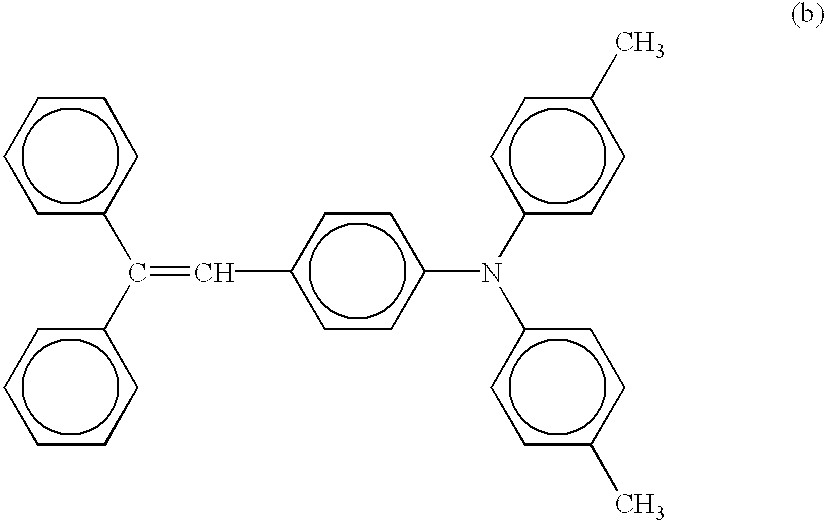
- a charge carrier transport layer in which a charge carrier transport material having the following formula (b) and a bisphenol type polycarbonate resin (trade name of PANLITE K-1300, manufactured by Teijin Ltd.) were included in a ratio of 1:1 by weight was formed on the charge carrier generation layer such that the thickness thereof was 10 ⁇ m.
- the thickness of the charge carrier transport layer was measured by sloan DEKTAK IIA as the difference from a standard plane.
- the electric field of the charge carrier transport layer can be calculated by the potential formed thereon and its thickness.
- Photoresponse of the photoreceptor to short pulse light was measured using an electrostatic paper analyzer EPA8200 (manufactured by Kawaguchi Electric Works) and a Xenon flash lamp module C5604 which serves as a pulse light source and which could emit pulse light having a half width of 3 ⁇ s.
- the amount of light radiated to the photoreceptor was changed using an ND filter to obtain the surface potential decay properties of the photoreceptor.
- the photoreceptor was charged so as to have a potential of about ⁇ 500 V and pulse light was radiated to the photoreceptor such that the potential decayed from ⁇ 500 V to about ⁇ 100 V.
- This surface potential decay curve of the photoreceptor was stored in a storage scope and then the time needed for decaying the initial potential ( ⁇ 500 V) to one-half ( ⁇ 250 V). This time is referred to as photoresponse of the photoreceptor.
- the photoresponse of the photoreceptor of Example 1 was 0.08 ms.
- the operation properties of the photoreceptor were checked using an electrophotographic process simulator, it was found that the photoreceptor could stably work at a speed of 200 mm/s.
- a photoreceptor which was prepared by repeating the procedure for preparation of the photoreceptor in Example 1 except that the substrate was changed to an aluminum cylinder having a diameter of 60 mm, was set in an electrophotographic copier, modified IMAGIO MF4550 manufactured by Ricoh Co., Ltd., to perform a copying test.
- the time from the imagewise light irradiation process to the developing process was about 100 ms.
- the photoreceptor produced images having good resolution.
- the resolution was 7.1 lines/mm.
- the charge mobility of the charge carrier transport layer was also measured when the electric field was 4.5 ⁇ 10 5 V/cm.
- the charge mobility in the charge carrier transport layer of the photoreceptor of Example 1 was 1 ⁇ 10 ⁇ 4 cm 2 /V ⁇ s.
- the ratio of the thickness (t CTL ) to the charge mobility ( ⁇ CTL ), t CTL / ⁇ CTL was 1 ⁇ 10 3 V ⁇ s/m.
- a charge carrier generation layer which consisted of a mixture of the charge carrier generation material having formula (a) described above and a charge carrier transport material having the following formula (c) in a ratio of 1:1 by weight, was formed on an aluminum substrate such that the thickness thereof was 0.21 ⁇ m.
- a charge carrier transport layer consisting of the charge carrier transport material having formula (c) was formed on the charge carrier transport layer such that the thickness thereof was 11 ⁇ m.
- the photoresponse of the photoreceptor was 0.03 ms.
- the operation properties of the photoreceptor were checked using the electrophotographic process simulator, it was found that the photoreceptor could stably work at a speed of 200 mm/s.
- the photoreceptor produced images having good resolution.
- the resolution was 6.3 lines/mm.
- the charge mobility of the charge carrier transport layer of the photoreceptor of Example 2 was 5 ⁇ 10 ⁇ 4 cm 2 /V ⁇ s under an electric field of 4.5 ⁇ 10 5 V/cm.
- the ratio of the thickness (t CTL ) to the charge mobility ( ⁇ CTL ), t CTL / ⁇ CTL was 2.2 ⁇ 10 2 V ⁇ s/m.
- Example 2 The procedure for preparation of the charge carrier generation layer in Example 1 was repeated. Then a charge carrier transport layer, which consisted of a mixture of the charge carrier transport material having formula (b) and the charge carrier transport material having formula (c) in a ratio of 1:1 was formed on the charge carrier generation layer such that the thickness thereof was 9 ⁇ m.
- the responsivity of the photoreceptor was 0.03 ms.
- the operation properties of the photoreceptor were checked using the electrophotographic process simulator, it was found that the photoreceptor could stably work at a speed of 200 mm/s.
- the photoreceptor produced images having good resolution and the resolution of the images was 6.3 lines/mm.
- the charge mobility of the charge carrier transport layer of the photoreceptor of Example 3 was 2 ⁇ 10 ⁇ 4 cm 2 /V ⁇ s under an electric field of 4.5 ⁇ 10 5 V/cm.
- the ratio of the thickness (t CTL ) to the charge mobility ( ⁇ CTL ), t CTL / ⁇ CTL was 4.5 ⁇ 10 2 V ⁇ s/m.
- a charge carrier generation layer which consisted of a mixture of a charge carrier generation material having the following formula (d) and a polyvinyl butyral resin (Trade name of XYHL, manufactured by Union Carbide Corp.) in a ratio of 3:1 by weight, was formed on an aluminum substrate such that the thickness thereof was, 0.2 ⁇ m.
- a charge carrier transport layer which consisted of a mixture of the charge carrier transport material having formula (c) and a polycarbonate resin (Trade name of PANLITE K-1300, manufactured by Teijin ltd.) in a ratio of 1:1 by weight was formed thereon such that the thickness thereof was 20 ⁇ m.
- the photoresponse of the photoreceptor was 1.2 ms.
- the operation properties of the photoreceptor were checked using the electrophotographic process simulator, it was found that the photoreceptor could not work at a speed of 200 mm/s because the photoreceptor had poor photosensitivity.
- the charge mobility of the charge carrier transport layer of the photoreceptor of Comparative Example 1 was 3 ⁇ 10 ⁇ 5 cm 2 /V ⁇ s under an electric field of 4.5 ⁇ 10 5 V/cm.
- the ratio of the thickness (t CTL ) to the charge mobility ( ⁇ CTL ), t CTL / ⁇ CTL was 6.7 ⁇ 10 3 V ⁇ s/m.
- Example 1 The procedure for preparation of the photoreceptor in Example 1 was repeated except that the composition of the charge carrier transport layer was a mixture of the charge carrier transport material having formula (b) and a bisphenol type polycarbonate resin (PANLITE K-1300) in a ratio of 3:7 by weight, and the thickness of the charge carrier transport layer was changed to 19 ⁇ m.
- the composition of the charge carrier transport layer was a mixture of the charge carrier transport material having formula (b) and a bisphenol type polycarbonate resin (PANLITE K-1300) in a ratio of 3:7 by weight, and the thickness of the charge carrier transport layer was changed to 19 ⁇ m.
- PANLITE K-1300 bisphenol type polycarbonate resin
- the photoresponse of the photoreceptor was 2.5 ms.
- the operation properties of the photoreceptor were checked using the electrophotographic process simulator, it was found that the photoreceptor could not work at a speed of 200 mm/s because the photoreceptor had poor photosensitivity.
- the charge mobility of the charge carrier transport layer of the photoreceptor of Comparative Example 2 was 2 ⁇ 10 ⁇ 5 cm 2 /V ⁇ s under an electric field of 4.5 ⁇ 10 5 V/cm.
- the ratio of the thickness (t CTL ) to the charge mobility ( ⁇ CTL ), t CTL / ⁇ CTL was 9.5 ⁇ 10 3 V ⁇ s/m.
- a charge carrier generation layer which consisted of a mixture of a charge carrier generation material consisting of an oxotitanium phthalocyanine pigment and a polyvinyl butyral resin (tradename of XYHL, manufactured by Union Carbide Corp.) in a ratio of 10:1 by weight, was formed on an aluminum substrate such that the thickness thereof was 0.2 ⁇ m.
- a charge carrier transport layer consisting of a high-molecular-weight charge carrier transport material having the following formula (e) was formed thereon such that the thickness thereof was 11 ⁇ m.
- the photoresponse of the photoreceptor was 0.7 ms.
- the operation properties of the photoreceptor were checked using the electrophotographic process simulator, it was found that the photoreceptor could work well at a speed of 200 mm/s because the photoreceptor had high photosensitivity.
- the photoreceptor produced images having good resolution.
- the resolution was 6.3 lines/mm.
- the charge mobility of the charge carrier transport layer of the photoreceptor of Example 4 was 1 ⁇ 10 ⁇ 4 cm 2 /V ⁇ s under an electric field of 4.5 ⁇ 10 5 V/cm.
- the ratio of the thickness (t CTL ) to the charge mobility ( ⁇ CTL ), t CTL / ⁇ CTL was 1.1 ⁇ 10 3 V ⁇ s/m.
- Example 1 The procedure for preparation of the photoreceptor in Example 1 was repeated except that a fluorine-containing oil (perfluoropolyether oil tradenamed as DMUNUMTM GREASE S-100, manufactured by Daikin Industries Ltd.) was added to the charge carrier transport layer in an amount of 0.2% by weight.
- a fluorine-containing oil perfluoropolyether oil tradenamed as DMUNUMTM GREASE S-100, manufactured by Daikin Industries Ltd.
- the photoresponse of the photoreceptor was 0.25 ms.
- the operation properties of the photoreceptor were checked using the electrophotographic process simulator, it was found that the photoreceptor could work well at a speed of 200 mm/s because the photoreceptor had high photosensitivity.
- the photoreceptor was subjected to a rubbing test, in which stress was applied to the photoreceptor corresponding to the stress applied to the photoreceptor when the photoreceptor was run in a copier so that 100,000 copies were formed, using a rubbing tester.
- the coefficient of friction between the photoreceptor and paper was not greater than 0.5.
- Example 2 The procedure for preparation of the photoreceptor in Example 2 was repeated except that a fluorine-containing oil (perfluoropolyether oil tradenamed as DEMNUMTM GREASE S-100, manufactured by Daikin Industries Ltd.) was added to the charge carrier transport layer in an amount of 0.2% by weight.
- a fluorine-containing oil perfluoropolyether oil tradenamed as DEMNUMTM GREASE S-100, manufactured by Daikin Industries Ltd.
- the photoresponse of the photoreceptor was 0.19 ms.
- the operation properties of the photoreceptor were checked using an electrophotographic process simulator, it was found that the photoreceptor could work well at a speed of 200 mm/s because the photoreceptor had high photosensitivity.
- the coefficient of friction between the photoreceptor and paper was not greater than 0.5.
- Example 3 The procedure for preparation of the photoreceptor in Example 3 was repeated except that zinc stearate was added to the charge carrier transport layer in an amount of 0.3% by weight.
- the photoresponse of the photoreceptor was 0.22 ms.
- the operation properties of the photoreceptor were checked using the electrophotographic process simulator, it was found that the photoreceptor could work well at a speed of 200 mm/s because the photoreceptor had high photosensitivity.
- the coefficient of friction between the photoreceptor and paper was not greater than 0.5.
- the photoreceptor of Comparative Example 1 was subjected to the abrasion test.
- the coefficient of friction between the photoreceptor and paper was not less than 0.6 even after an abrasion test corresponding to a 100-copies running test in a copier.
- the photoreceptor of Comparative Example 2 was subjected to the abrasion test.
- the coefficient of friction between the photoreceptor and paper was not less than 0.6 even after an abrasion test corresponding to a 100-copies running test in a copier.
- Example 4 The procedure for preparation of the photoreceptor in Example 4 was repeated except that zinc stearate was added to the charge carrier transport layer in an amount of 0.3% by weight.
- the responsivity of the photoreceptor was 0.83 ms.
- the operation properties of the photoreceptor were checked using an electrophotographic process simulator, it was found that the photoreceptor could work well at a speed of 200 mm/s because the photoreceptor had high photosensitivity.
- the coefficient of friction between the photoreceptor and paper was not greater than 0.5.
- the cylindrical photoreceptor of Example 1 was set in a copying tester, in which a member imparting low friction coefficient to the photoreceptor and always contacting the photoreceptor was provided between a cleaning unit and a charger.
- the member was constituted of a stainless substrate, an urethane foam (Trade name of LE20, manufactured by INOAC Corp.) formed on the stainless substrate, and a PTFE sheet (tradename of T/#9001, manufactured by Nichias Corp.) formed on the urethane foam.
- the photoreceptor of Example 2 was subjected to the running test described in Example 9. Even after the running test, the coefficient of friction between the photoreceptor and paper was not greater than 0.5.
- Example 3 The photoreceptor of Example 3 was subjected to the running test described in Example 9 except that the member imparting low friction coefficient to the photoreceptor was replaced with a member in which a “PTFE” powder (RUBRON L2 manufactured by Daikin Industries Ltd. ) was supplied to a brush to supply the powder to the photoreceptor while the brush was rotated in a direction opposite to the rotating direction of the photoreceptor.
- a “PTFE” powder RABRON L2 manufactured by Daikin Industries Ltd.
- the photoreceptor of Example 4 was subjected to the running test described in Example 11. Even after the running test, the coefficient of friction between the photoreceptor and paper was not greater than 0.5.
- the photoreceptor of the present invention have so high photosensitivity that the photoreceptor can produce good image even when used for high speed copiers, because of having a property such that a ratio of the thickness (t) of the charge carrier transport layer to the charge mobility ( ⁇ ) thereof is not greater than 1.5 ⁇ 10 3 .
- a lubricant in a top layer of the photoreceptor which is used for producing images having good resolution and which has a relatively thin photoreceptive layer, or by supplying a lubricant to the photoreceptor in a copier, the photoreceptor has good resistance to abrasion and therefore can produce good images even upon use for a long period of time.
Landscapes
- Physics & Mathematics (AREA)
- General Physics & Mathematics (AREA)
- Spectroscopy & Molecular Physics (AREA)
- Chemical & Material Sciences (AREA)
- Chemical Kinetics & Catalysis (AREA)
- Health & Medical Sciences (AREA)
- Emergency Medicine (AREA)
- Photoreceptors In Electrophotography (AREA)
Abstract
Description


Claims (18)


Applications Claiming Priority (2)
| Application Number | Priority Date | Filing Date | Title |
|---|---|---|---|
| JP11-037691 | 1999-02-16 | ||
| JP3769199 | 1999-02-16 |
Publications (1)
| Publication Number | Publication Date |
|---|---|
| US6521386B1 true US6521386B1 (en) | 2003-02-18 |
Family
ID=12504596
Family Applications (1)
| Application Number | Title | Priority Date | Filing Date |
|---|---|---|---|
| US09/504,799 Expired - Fee Related US6521386B1 (en) | 1999-02-16 | 2000-02-15 | Electrophotographic photoreceptor and electrophotographic image forming method and apparatus using the photoreceptor |
Country Status (1)
| Country | Link |
|---|---|
| US (1) | US6521386B1 (en) |
Cited By (27)
| Publication number | Priority date | Publication date | Assignee | Title |
|---|---|---|---|---|
| US20030175046A1 (en) * | 2002-01-17 | 2003-09-18 | Akiyo Namiki | Charging device, process cartridge and image forming apparatus |
| US20030207771A1 (en) * | 2002-05-02 | 2003-11-06 | Lester Cornelius | Cleaning blade lubricant |
| US20030207770A1 (en) * | 2002-05-02 | 2003-11-06 | Lester Cornelius | Cleaning blade lubricant |
| US20030219279A1 (en) * | 2002-03-13 | 2003-11-27 | Shinji Nohsho | Image-forming apparatus and image-forming process-cartridge |
| US6706459B2 (en) | 1999-04-08 | 2004-03-16 | Ricoh Company, Ltd. | Electrophotographic drum-shaped photoconductor and image forming method and apparatus using the same |
| US20040096239A1 (en) * | 2002-08-09 | 2004-05-20 | Hiroshi Hosokawa | Image forming apparatus and process cartridge removably mounted thereto |
| US20040131381A1 (en) * | 2002-09-19 | 2004-07-08 | Masanori Kawasumi | Image forming apparatus and process cartridge |
| US20040170446A1 (en) * | 2002-12-20 | 2004-09-02 | Hiroyuki Nagashima | Image forming apparatus using a user installable process cartridge, a method of arranging the process cartridge, and the process cartridge itself |
| US20040234294A1 (en) * | 2003-02-28 | 2004-11-25 | Hiroshi Nagame | Image forming apparatus, process cartridge, and image forming method |
| US20050078991A1 (en) * | 2003-08-26 | 2005-04-14 | Yoshiyuki Kimura | Cleaning apparatus for removing toner adhered onto endless belt |
| US20050141919A1 (en) * | 2003-12-25 | 2005-06-30 | Ryoichi Kitajima | Image forming apparatus and image forming method |
| US20050153222A1 (en) * | 2004-01-14 | 2005-07-14 | Sharp Kabushiki Kaisha | Electrophotographic photoreceptor and image forming device incorporating same |
| US20050158644A1 (en) * | 2003-12-09 | 2005-07-21 | Maiko Kondo | Toner, developer, toner container and latent electrostatic image carrier, and process cartridge, image forming method, and image forming apparatus using the same |
| US20050181291A1 (en) * | 2004-01-08 | 2005-08-18 | Hidetoshi Kami | Electrophotographic photoconductor, preparation method thereof, electrophotographic apparatus and process cartridge |
| US20050226656A1 (en) * | 2002-09-24 | 2005-10-13 | Kiyonori Tsuda | Image forming apparatus using a toner container and a process cartridge |
| US20050238977A1 (en) * | 2000-03-02 | 2005-10-27 | Narihito Kojima | Electrophotographic photoreceptor and image forming apparatus using the photoreceptor |
| US7076192B2 (en) | 2002-12-27 | 2006-07-11 | Ricoh Company, Ltd. | Powder conveying device and image forming apparatus using the same |
| US20070026330A1 (en) * | 2005-07-28 | 2007-02-01 | Xerox Corporation | Photoreceptor layer having solid and liquid lubricants |
| US20070077100A1 (en) * | 2004-02-06 | 2007-04-05 | Masato Suzuki | Toner bottle, process for producing the same, toner container, and toner cartridge, and, image forming apparatus and image forming process |
| US20070177905A1 (en) * | 2003-02-28 | 2007-08-02 | Hiroshi Hosokawa | Developer container, developer supplying device, and image forming apparatus |
| US7466945B2 (en) | 2004-03-05 | 2008-12-16 | Ricoh Company, Ltd. | Toner container, toner replenishing device, developing device, process cartridge and image forming apparatus |
| US20090123192A1 (en) * | 2004-08-16 | 2009-05-14 | Nobuyuki Taguchi | Method and toner bottle for image forming apparatus capable of effectively supplying toner to image forming apparatus |
| US9207624B2 (en) | 2014-01-27 | 2015-12-08 | Ricoh Company, Ltd. | Cleaning blade, method for preparing the cleaning blade, and image forming apparatus and process cartridge using the cleaning blade |
| US9244423B2 (en) | 2014-03-13 | 2016-01-26 | Ricoh Company, Ltd. | Cleaning blade, and image forming apparatus and process cartridge using the cleaning blade |
| US9395676B2 (en) | 2014-03-07 | 2016-07-19 | Ricoh Company, Ltd. | Cleaning blade having an elastic body of segmented hardnesses, and image forming apparatus and process cartridge including the cleaning blade |
| US9746817B2 (en) | 2013-11-15 | 2017-08-29 | Ricoh Company, Ltd. | Cleaning blade with elastic member including reformed layer, image forming apparatus, and process cartridge with the same |
| US10146169B2 (en) | 2016-07-15 | 2018-12-04 | Ricoh Company, Ltd. | Cleaning blade, process cartridge, and image forming apparatus |
Citations (12)
| Publication number | Priority date | Publication date | Assignee | Title |
|---|---|---|---|---|
| US4435074A (en) * | 1980-04-23 | 1984-03-06 | Ricoh Company, Ltd. | Cleaning apparatus for electrophotography comprising lubricant film applicator means |
| US5206103A (en) * | 1991-01-14 | 1993-04-27 | Xerox Corporation | Photoconductive imaging member with a charge transport layer comprising a biphenyl diamine and a polysilylane |
| JPH05165244A (en) * | 1991-12-13 | 1993-07-02 | Ricoh Co Ltd | Electrophotographic sensitive body |
| US5350653A (en) | 1992-03-02 | 1994-09-27 | Ricoh Company, Ltd. | Electrophotographic photoconductor |
| US5409792A (en) * | 1991-08-26 | 1995-04-25 | Xerox Corporation | Photoreceptor containing dissimilar charge transporting small molecule and charge transporting polymer |
| US5492784A (en) | 1992-08-07 | 1996-02-20 | Ricoh Company, Ltd. | Positively-chargeable single-layered type electrophotographic photoconductor |
| US5504559A (en) * | 1993-08-30 | 1996-04-02 | Minolta Co., Ltd. | Method for image formation |
| US5874876A (en) | 1995-12-28 | 1999-02-23 | Niles Parts Co., Ltd. | Electromagnetic relay structure |
| US5908725A (en) * | 1992-12-28 | 1999-06-01 | Minolta Co., Ltd. | Photosensitive member comprising thick photosensitive layer formed on anodized aluminum layer |
| US5942360A (en) * | 1998-03-31 | 1999-08-24 | Xerox Corporation | Photoreceptor with low surface energy and process of making |
| US6030734A (en) * | 1996-03-11 | 2000-02-29 | Mitsubishi Chemical Corporation | Electrophotographic photoreceptor containing charge-transporting material with butadiene structure |
| US6030733A (en) * | 1998-02-03 | 2000-02-29 | Ricoh Company, Ltd. | Electrophotographic photoconductor with water vapor permeability |
-
2000
- 2000-02-15 US US09/504,799 patent/US6521386B1/en not_active Expired - Fee Related
Patent Citations (13)
| Publication number | Priority date | Publication date | Assignee | Title |
|---|---|---|---|---|
| US4435074A (en) * | 1980-04-23 | 1984-03-06 | Ricoh Company, Ltd. | Cleaning apparatus for electrophotography comprising lubricant film applicator means |
| US5206103A (en) * | 1991-01-14 | 1993-04-27 | Xerox Corporation | Photoconductive imaging member with a charge transport layer comprising a biphenyl diamine and a polysilylane |
| US5409792A (en) * | 1991-08-26 | 1995-04-25 | Xerox Corporation | Photoreceptor containing dissimilar charge transporting small molecule and charge transporting polymer |
| JPH05165244A (en) * | 1991-12-13 | 1993-07-02 | Ricoh Co Ltd | Electrophotographic sensitive body |
| US5350653A (en) | 1992-03-02 | 1994-09-27 | Ricoh Company, Ltd. | Electrophotographic photoconductor |
| US5486438A (en) | 1992-03-02 | 1996-01-23 | Ricoh Company, Ltd. | Electrophotographic photoconductor |
| US5492784A (en) | 1992-08-07 | 1996-02-20 | Ricoh Company, Ltd. | Positively-chargeable single-layered type electrophotographic photoconductor |
| US5908725A (en) * | 1992-12-28 | 1999-06-01 | Minolta Co., Ltd. | Photosensitive member comprising thick photosensitive layer formed on anodized aluminum layer |
| US5504559A (en) * | 1993-08-30 | 1996-04-02 | Minolta Co., Ltd. | Method for image formation |
| US5874876A (en) | 1995-12-28 | 1999-02-23 | Niles Parts Co., Ltd. | Electromagnetic relay structure |
| US6030734A (en) * | 1996-03-11 | 2000-02-29 | Mitsubishi Chemical Corporation | Electrophotographic photoreceptor containing charge-transporting material with butadiene structure |
| US6030733A (en) * | 1998-02-03 | 2000-02-29 | Ricoh Company, Ltd. | Electrophotographic photoconductor with water vapor permeability |
| US5942360A (en) * | 1998-03-31 | 1999-08-24 | Xerox Corporation | Photoreceptor with low surface energy and process of making |
Non-Patent Citations (10)
| Title |
|---|
| Derwent Machine-Assisted Translation of JP 5-165244 (pub 7/93).* * |
| Jap 10 Abstract of JP 05-165244, pub Jul. 2, 1993.* * |
| JPO Abstract oF JP 04287052A, Oct. 12, 1992. |
| JPO Abstract of JP 05165384A, Jul. 2, 1993. |
| JPO Abstract of JP 06342236 A, Dec. 13, 1994. |
| JPO Abstract of JP 08006450A, Jan. 12, 1996. |
| JPO Abstract of JP 08062862A, Mar. 8, 1996. |
| JPO Abstract of JP 08272198A, Oct. 18, 1996. |
| JPO Abstract of JP 09081001A, Mar. 28, 1997. |
| U.S. Trademark Electronic Search System (TESS) Search of Panlite, which was registered Aug. 4, 1987.* * |
Cited By (60)
| Publication number | Priority date | Publication date | Assignee | Title |
|---|---|---|---|---|
| US6706459B2 (en) | 1999-04-08 | 2004-03-16 | Ricoh Company, Ltd. | Electrophotographic drum-shaped photoconductor and image forming method and apparatus using the same |
| US20050238977A1 (en) * | 2000-03-02 | 2005-10-27 | Narihito Kojima | Electrophotographic photoreceptor and image forming apparatus using the photoreceptor |
| US7153621B2 (en) | 2000-03-02 | 2006-12-26 | Ricoh Company Limited | Electrophotographic photoreceptor and image forming apparatus using the photoreceptor |
| US20030175046A1 (en) * | 2002-01-17 | 2003-09-18 | Akiyo Namiki | Charging device, process cartridge and image forming apparatus |
| US20030219279A1 (en) * | 2002-03-13 | 2003-11-27 | Shinji Nohsho | Image-forming apparatus and image-forming process-cartridge |
| US6879799B2 (en) | 2002-03-13 | 2005-04-12 | Ricoh Company, Ltd. | Image-forming apparatus and image-forming process-cartridge |
| US6869918B2 (en) * | 2002-05-02 | 2005-03-22 | Lester Cornelius | Cleaning blade lubricant |
| US20030207771A1 (en) * | 2002-05-02 | 2003-11-06 | Lester Cornelius | Cleaning blade lubricant |
| US20030207770A1 (en) * | 2002-05-02 | 2003-11-06 | Lester Cornelius | Cleaning blade lubricant |
| US7212767B2 (en) | 2002-08-09 | 2007-05-01 | Ricoh Company, Ltd. | Image forming apparatus and process cartridge removably mounted thereto |
| US20040096239A1 (en) * | 2002-08-09 | 2004-05-20 | Hiroshi Hosokawa | Image forming apparatus and process cartridge removably mounted thereto |
| US7003255B2 (en) | 2002-09-19 | 2006-02-21 | Ricoh Company, Ltd. | Image forming apparatus and process cartridge |
| US20040131381A1 (en) * | 2002-09-19 | 2004-07-08 | Masanori Kawasumi | Image forming apparatus and process cartridge |
| US7398038B2 (en) | 2002-09-24 | 2008-07-08 | Ricoh Company, Ltd. | Image forming apparatus using a toner container and a process cartridge |
| US20050226656A1 (en) * | 2002-09-24 | 2005-10-13 | Kiyonori Tsuda | Image forming apparatus using a toner container and a process cartridge |
| US20040170446A1 (en) * | 2002-12-20 | 2004-09-02 | Hiroyuki Nagashima | Image forming apparatus using a user installable process cartridge, a method of arranging the process cartridge, and the process cartridge itself |
| US7024133B2 (en) | 2002-12-20 | 2006-04-04 | Ricoh Co., Ltd. | Image forming apparatus using a user installable process cartridge, a method of arranging the process cartridge, and the process cartridge itself |
| US7076192B2 (en) | 2002-12-27 | 2006-07-11 | Ricoh Company, Ltd. | Powder conveying device and image forming apparatus using the same |
| US20040234294A1 (en) * | 2003-02-28 | 2004-11-25 | Hiroshi Nagame | Image forming apparatus, process cartridge, and image forming method |
| US7835673B2 (en) | 2003-02-28 | 2010-11-16 | Ricoh Company, Ltd. | Developer container, developer supplying device, and image forming apparatus |
| US20110026973A1 (en) * | 2003-02-28 | 2011-02-03 | Hiroshi Hosokawa | Developer container, developer supplying device, and image forming apparatus |
| US8005406B2 (en) | 2003-02-28 | 2011-08-23 | Ricoh Company, Ltd. | Developer container, developer supplying device, and image forming apparatus |
| US7697870B2 (en) | 2003-02-28 | 2010-04-13 | Ricoh Company, Ltd. | Developer container, developer supplying device, and image forming apparatus |
| US7177570B2 (en) | 2003-02-28 | 2007-02-13 | Ricoh Company, Limited | Measurement of frictional resistance of photoconductor against belt in image forming apparatus, process cartridge, and image forming method |
| US20090175660A1 (en) * | 2003-02-28 | 2009-07-09 | Hiroshi Hosokawa | Developer container, developer supplying device, and image forming apparatus |
| US8195070B2 (en) | 2003-02-28 | 2012-06-05 | Ricoh Company, Ltd. | Developer container, developer supplying device, and image forming apparatus |
| US20070177905A1 (en) * | 2003-02-28 | 2007-08-02 | Hiroshi Hosokawa | Developer container, developer supplying device, and image forming apparatus |
| US7519317B2 (en) | 2003-02-28 | 2009-04-14 | Ricoh Company, Ltd. | Developer container, developer supplying device, and image forming apparatus |
| US7480476B2 (en) | 2003-02-28 | 2009-01-20 | Ricoh Company, Ltd. | Developer container, developer supplying device, and image forming apparatus |
| US20080003021A1 (en) * | 2003-02-28 | 2008-01-03 | Hiroshi Hosokawa | Developer container, developer supplying device, and image forming apparatus |
| US20080286013A1 (en) * | 2003-02-28 | 2008-11-20 | Hiroshi Hosokawa | Developer container, developer supplying device, and image forming apparatus |
| US20050078991A1 (en) * | 2003-08-26 | 2005-04-14 | Yoshiyuki Kimura | Cleaning apparatus for removing toner adhered onto endless belt |
| US7421239B2 (en) | 2003-08-26 | 2008-09-02 | Ricoh Company, Ltd. | Cleaning apparatus for removing toner adhered onto endless belt |
| US7386256B2 (en) | 2003-12-09 | 2008-06-10 | Ricoh Company, Ltd. | Toner, developer, toner container and latent electrostatic image carrier, and process cartridge, image forming method, and image forming apparatus using the same |
| US20080193865A1 (en) * | 2003-12-09 | 2008-08-14 | Maiko Kondo | Toner, developer, toner container and latent electrostatic image carrier, and process cartridge, image forming method, and image forming apparatus using the same |
| US7482104B2 (en) | 2003-12-09 | 2009-01-27 | Ricoh Company, Ltd. | Toner, developer, toner container and latent electrostatic image carrier, and process cartridge, image forming method, and image forming apparatus using the same |
| US20050158644A1 (en) * | 2003-12-09 | 2005-07-21 | Maiko Kondo | Toner, developer, toner container and latent electrostatic image carrier, and process cartridge, image forming method, and image forming apparatus using the same |
| US7315722B2 (en) | 2003-12-25 | 2008-01-01 | Ricoh Company, Ltd. | Image forming apparatus and image forming method |
| US20050141919A1 (en) * | 2003-12-25 | 2005-06-30 | Ryoichi Kitajima | Image forming apparatus and image forming method |
| US7341814B2 (en) | 2004-01-08 | 2008-03-11 | Ricoh Company, Ltd. | Electrophotographic photoconductor, preparation method thereof, electrophotographic apparatus and process cartridge |
| US20050181291A1 (en) * | 2004-01-08 | 2005-08-18 | Hidetoshi Kami | Electrophotographic photoconductor, preparation method thereof, electrophotographic apparatus and process cartridge |
| US7449269B2 (en) | 2004-01-14 | 2008-11-11 | Sharp Kabushiki Kaisha | Electrophotographic photoreceptor having defined mobility of electric charges in photosensitive layer and image forming device incorporating same |
| US20050153222A1 (en) * | 2004-01-14 | 2005-07-14 | Sharp Kabushiki Kaisha | Electrophotographic photoreceptor and image forming device incorporating same |
| US7313349B2 (en) | 2004-02-06 | 2007-12-25 | Ricoh Company, Ltd. | Toner container and image forming apparatus |
| US20070077100A1 (en) * | 2004-02-06 | 2007-04-05 | Masato Suzuki | Toner bottle, process for producing the same, toner container, and toner cartridge, and, image forming apparatus and image forming process |
| US7466945B2 (en) | 2004-03-05 | 2008-12-16 | Ricoh Company, Ltd. | Toner container, toner replenishing device, developing device, process cartridge and image forming apparatus |
| US7747202B2 (en) | 2004-08-16 | 2010-06-29 | Ricoh Company, Ltd. | Method and toner bottle for image forming apparatus capable of effectively supplying toner to image forming apparatus |
| US20100254732A1 (en) * | 2004-08-16 | 2010-10-07 | Nobuyuki Taguchi | Method and toner bottle for image forming apparatus capable of effectively supplying toner to image forming apparatus |
| US7720416B2 (en) | 2004-08-16 | 2010-05-18 | Ricoh Company, Ltd. | Method and toner bottle for image forming apparatus capable of effectively supplying toner to image forming apparatus |
| US7840167B2 (en) | 2004-08-16 | 2010-11-23 | Ricoh Company, Ltd. | Toner container including a gear which is at least partially exposed to an exterior |
| US8396398B2 (en) | 2004-08-16 | 2013-03-12 | Ricoh Company, Ltd. | Method and toner bottle for image forming apparatus capable of effectively supplying toner to image forming apparatus |
| US20090123192A1 (en) * | 2004-08-16 | 2009-05-14 | Nobuyuki Taguchi | Method and toner bottle for image forming apparatus capable of effectively supplying toner to image forming apparatus |
| US8121525B2 (en) | 2004-08-16 | 2012-02-21 | Ricoh Company, Ltd. | Method and toner bottle for image forming apparatus capable of effectively supplying toner to image forming apparatus |
| US7527902B2 (en) * | 2005-07-28 | 2009-05-05 | Xerox Corporation | Photoreceptor layer having solid and liquid lubricants |
| US20070026330A1 (en) * | 2005-07-28 | 2007-02-01 | Xerox Corporation | Photoreceptor layer having solid and liquid lubricants |
| US9746817B2 (en) | 2013-11-15 | 2017-08-29 | Ricoh Company, Ltd. | Cleaning blade with elastic member including reformed layer, image forming apparatus, and process cartridge with the same |
| US9207624B2 (en) | 2014-01-27 | 2015-12-08 | Ricoh Company, Ltd. | Cleaning blade, method for preparing the cleaning blade, and image forming apparatus and process cartridge using the cleaning blade |
| US9395676B2 (en) | 2014-03-07 | 2016-07-19 | Ricoh Company, Ltd. | Cleaning blade having an elastic body of segmented hardnesses, and image forming apparatus and process cartridge including the cleaning blade |
| US9244423B2 (en) | 2014-03-13 | 2016-01-26 | Ricoh Company, Ltd. | Cleaning blade, and image forming apparatus and process cartridge using the cleaning blade |
| US10146169B2 (en) | 2016-07-15 | 2018-12-04 | Ricoh Company, Ltd. | Cleaning blade, process cartridge, and image forming apparatus |
Similar Documents
| Publication | Publication Date | Title |
|---|---|---|
| US6521386B1 (en) | Electrophotographic photoreceptor and electrophotographic image forming method and apparatus using the photoreceptor | |
| US6558862B2 (en) | Electrophotographic photoreceptor and image forming apparatus using the photoreceptor | |
| JP2002341578A (en) | Image forming device | |
| US7842443B2 (en) | Method for evaluating electrophotographic photoconductor and the evaluation device, and method for reusing electrophotographic photoconductor | |
| JP3874328B2 (en) | Electrophotographic photoreceptor and image forming method and apparatus using the same | |
| JP3927930B2 (en) | Electrophotographic photosensitive member, process cartridge, and electrophotographic apparatus | |
| JP2019139225A (en) | Electrophotographic photoreceptor, process cartridge and electrophotographic apparatus | |
| JP2000352832A (en) | Electrophotographic photoreceptor, image forming method and device using the same and method for applying lubricant substance to surface of the electrophotographic photoreceptor | |
| JP2004117766A (en) | Electrophotographic photoreceptor and image forming method using the same | |
| JP4223671B2 (en) | Electrophotographic photosensitive member, electrophotographic method, electrophotographic apparatus, and process cartridge for electrophotographic apparatus | |
| JP5970869B2 (en) | Electrophotographic photoreceptor, image forming method, process cartridge for image forming apparatus, and image forming apparatus | |
| JP6781396B2 (en) | Photoreceptor, image forming apparatus and process cartridge | |
| JP4711647B2 (en) | Electrophotographic photoreceptor, process cartridge using the same, and image forming apparatus | |
| JP4397328B2 (en) | Electrophotographic photosensitive member, image forming apparatus using the same, and process cartridge | |
| US9864322B2 (en) | Image forming apparatus | |
| JP4140473B2 (en) | Electrophotographic photosensitive member, image forming apparatus, and process cartridge | |
| JP2005266036A (en) | Photoreceptor, electrophotographing apparatus, and process cartridge for electrophotograhying apparatus | |
| JP2005070748A (en) | Electrophotographic photoreceptor, and process cartridge and image forming apparatus using same | |
| JP2000250245A (en) | Electrophotographic device and process cartridge used in same | |
| JP2005227470A (en) | Electrophotographic apparatus and process cartridge | |
| JP4602125B2 (en) | Method for predicting reduction in film thickness of image carrier, method for setting film thickness of image carrier, method for manufacturing process cartridge, and method for manufacturing image forming apparatus | |
| JP2002287387A (en) | Image forming method, image forming device and electrophotographic sensitive body | |
| JP2023164042A (en) | Electrophotographic photoreceptor, process cartridge, and electrophotographic device | |
| JP2023170538A (en) | Photoreceptor, process cartridge, and image forming method, and method for manufacturing photoreceptor | |
| JP2003195536A (en) | Electrophotographic photoreceptor, process cartridge and electrophotographic device |
Legal Events
| Date | Code | Title | Description |
|---|---|---|---|
| AS | Assignment |
Owner name: RICOH COMPANY, LTD., JAPAN Free format text: ASSIGNMENT OF ASSIGNORS INTEREST;ASSIGNORS:SAKON, YOHTA;KOJIMA, NARIHITO;UMEDA, MINORU;AND OTHERS;REEL/FRAME:010865/0543;SIGNING DATES FROM 20000209 TO 20000215 |
|
| AS | Assignment |
Owner name: RICOH COMPANY LTD., JAPAN Free format text: ASSIGNMENT OF ASSIGNORS INTEREST;ASSIGNORS:SAKON, YOHTA;KOJIMA, NARIHITO;UMEDA, MINORU;AND OTHERS;REEL/FRAME:013502/0959;SIGNING DATES FROM 20021105 TO 20021108 |
|
| AS | Assignment |
Owner name: RICOH COMPANY LTD., JAPAN Free format text: CORRECTIVE ASSIGNMENT TO CORRECT THE 4TH AND 5TH ASSIGNORS. DOCUMENT PREVIOUSLY RECORDED AT REEL 013502 FRAME 0959;ASSIGNORS:SAKON, YOHTA;KOJIMA, NARIHITO;UMEDA, MINORU;AND OTHERS;REEL/FRAME:013941/0488;SIGNING DATES FROM 20021105 TO 20021108 |
|
| FEPP | Fee payment procedure |
Free format text: PAYOR NUMBER ASSIGNED (ORIGINAL EVENT CODE: ASPN); ENTITY STATUS OF PATENT OWNER: LARGE ENTITY Free format text: PAYER NUMBER DE-ASSIGNED (ORIGINAL EVENT CODE: RMPN); ENTITY STATUS OF PATENT OWNER: LARGE ENTITY |
|
| FPAY | Fee payment |
Year of fee payment: 4 |
|
| FEPP | Fee payment procedure |
Free format text: PAYOR NUMBER ASSIGNED (ORIGINAL EVENT CODE: ASPN); ENTITY STATUS OF PATENT OWNER: LARGE ENTITY Free format text: PAYER NUMBER DE-ASSIGNED (ORIGINAL EVENT CODE: RMPN); ENTITY STATUS OF PATENT OWNER: LARGE ENTITY |
|
| FPAY | Fee payment |
Year of fee payment: 8 |
|
| REMI | Maintenance fee reminder mailed | ||
| LAPS | Lapse for failure to pay maintenance fees | ||
| STCH | Information on status: patent discontinuation |
Free format text: PATENT EXPIRED DUE TO NONPAYMENT OF MAINTENANCE FEES UNDER 37 CFR 1.362 |
|
| FP | Lapsed due to failure to pay maintenance fee |
Effective date: 20150218 |