US6496748B1 - Wafer flattening process and storage medium - Google Patents
Wafer flattening process and storage medium Download PDFInfo
- Publication number
- US6496748B1 US6496748B1 US09/234,937 US23493799A US6496748B1 US 6496748 B1 US6496748 B1 US 6496748B1 US 23493799 A US23493799 A US 23493799A US 6496748 B1 US6496748 B1 US 6496748B1
- Authority
- US
- United States
- Prior art keywords
- wafer
- nozzle
- outer rim
- speed
- data
- Prior art date
- Legal status (The legal status is an assumption and is not a legal conclusion. Google has not performed a legal analysis and makes no representation as to the accuracy of the status listed.)
- Expired - Fee Related
Links
Images


Classifications
-
- H—ELECTRICITY
- H01—ELECTRIC ELEMENTS
- H01L—SEMICONDUCTOR DEVICES NOT COVERED BY CLASS H10
- H01L21/00—Processes or apparatus adapted for the manufacture or treatment of semiconductor or solid state devices or of parts thereof
- H01L21/67—Apparatus specially adapted for handling semiconductor or electric solid state devices during manufacture or treatment thereof; Apparatus specially adapted for handling wafers during manufacture or treatment of semiconductor or electric solid state devices or components ; Apparatus not specifically provided for elsewhere
- H01L21/67005—Apparatus not specifically provided for elsewhere
- H01L21/67011—Apparatus for manufacture or treatment
- H01L21/67017—Apparatus for fluid treatment
- H01L21/67063—Apparatus for fluid treatment for etching
- H01L21/67069—Apparatus for fluid treatment for etching for drying etching
-
- H—ELECTRICITY
- H01—ELECTRIC ELEMENTS
- H01L—SEMICONDUCTOR DEVICES NOT COVERED BY CLASS H10
- H01L21/00—Processes or apparatus adapted for the manufacture or treatment of semiconductor or solid state devices or of parts thereof
- H01L21/02—Manufacture or treatment of semiconductor devices or of parts thereof
- H01L21/04—Manufacture or treatment of semiconductor devices or of parts thereof the devices having at least one potential-jump barrier or surface barrier, e.g. PN junction, depletion layer or carrier concentration layer
- H01L21/18—Manufacture or treatment of semiconductor devices or of parts thereof the devices having at least one potential-jump barrier or surface barrier, e.g. PN junction, depletion layer or carrier concentration layer the devices having semiconductor bodies comprising elements of Group IV of the Periodic System or AIIIBV compounds with or without impurities, e.g. doping materials
- H01L21/30—Treatment of semiconductor bodies using processes or apparatus not provided for in groups H01L21/20 - H01L21/26
- H01L21/302—Treatment of semiconductor bodies using processes or apparatus not provided for in groups H01L21/20 - H01L21/26 to change their surface-physical characteristics or shape, e.g. etching, polishing, cutting
- H01L21/306—Chemical or electrical treatment, e.g. electrolytic etching
- H01L21/30625—With simultaneous mechanical treatment, e.g. mechanico-chemical polishing
Definitions
- the present invention relates to a wafer flattening process for locally etching projecting portions on the surface of a wafer by an activated species gas to flatten the same or locally etching relatively thick portions of the wafer to make the distribution of thickness of the wafer uniform and to a storage medium for the same.
- FIG. 9 is a schematic sectional view of an example of a wafer flattening process of the related art.
- reference numeral 100 is a plasma generator.
- the plasma generator 100 sprays the activated species gas G generated in the plasma from a nozzle 101 to the surface of the wafer W.
- the wafer W is placed on and affixed to a stage 120 .
- the stage 120 is made to move in the horizontal direction so as to guide the portion Wa relatively thicker than the prescribed thickness on the surface of the wafer W (hereinafter referred to as the “relatively thick portion”) directly under the nozzle 101 .
- the activated species gas G is sprayed from the nozzle 101 to the projecting relatively thick portion Wa to locally etch the relatively thick portion Wa and make the distribution of thickness of the surface of the wafer W uniform.
- the thickness of the relatively thick portion Wa of the wafer W is also not uniform, but is diverse.
- This technology calls for the positions and thicknesses of the relatively thick portions Wa to be measured over the entire surface of the wafer W by a wafer flatness measuring device and for two-dimensional data of the positions and thicknesses to be prepared. The data is then converted to position-relative speed data showing the positions of the relatively thick portions Wa and the relative speed of the nozzle 101 by which the relatively thick portions Wa become the desired flatness after etching.
- the stage 120 is controlled based on this position-relative speed data to move the nozzle directly above the predetermined relatively thick portions Wa to etch the entire surface of the wafer W.
- the relative speed of the nozzle 101 is slowed to increase the amount of etching, while at locations of relatively thick portions Wa with small thicknesses, the relative speed of the nozzle 101 is increased to reduce the amount of etching, whereby the entire surface of the wafer W is flattened.
- FIG. 10 is a view of the state of spraying of the activated species gas G from the nozzle 101
- FIG. 11 is a schematic view for explaining the flattening operation by superposition of the activated species gas G
- FIG. 12 is a schematic sectional view for explaining the problem in the wafer flattening process of the related art.
- the activated species gas G sprayed from the nozzle 101 spreads out as it heads downward.
- the portion of the wafer W directly beneath the nozzle 101 is therefore etched deeply, while the portions away from that are etched shallowly.
- the nozzle 101 is scanning the surface, as shown in FIG. 11, the area Wb of the wafer W starts to be etched by the activated species gas G sprayed from the nozzle 101 then heading toward the area Wb.
- the area Wb is etched by the activated species gas G from the nozzle 101 moving from the position Q 1 toward the position Q 2 and is not affected by the activated species gas G at the pont of time when the nozzle 101 reaches the position Q 2 .
- the area Wb is etched by the superposition of the activated species gas G of the nozzle 101 moving between the positions Q 1 to Q 2 .
- the relative speed of the nozzle 101 moving between the positions Q 1 and Q 2 becomes slower in accordance with that thickness, while when the relatively thick portion of the area Wb is thin, the relative speed becomes faster, whereby the area Wb is etched flat.
- the nozzle 101 scans from the outside to the inside of the outer rim Wc, the nozzle 101 is moved at a high speed at the outside of the outer rim Wc and changes in relative speed in accordance with the thickness of the outer rim Wc when it reaches the position of the outer rim Wc, so the outer rim Wc is not affected much at all by the activated species gas G of the nozzle 101 when moving from the left.
- the present invention was made to solve the above problems and has as its object to provide a wafer flattening process designed to flatten the entire surface of the wafer including the outer rim of the wafer by inserting dummy data corresponding to the data of the outer rim of the wafer in the data of the outside of the wafer and to provide a storage medium for the same.
- a wafer flattening process which causes a nozzle to scan the entire surface of a wafer based on position-speed data comprised of coordinates on a plane including the surface of the wafer and a nozzle relative speed set substantially inversely proportionally to the value of thickness of the wafer at those coordinates and flattens the wafer by activated species gas sprayed from the nozzle, the wafer flattening process comprising the steps of: using, as dummy data, position-speed data outside of a predetermined area set on the wafer closest to an imaginary line extending from the center of the wafer in the radial direction; and setting the nozzle relative speed of the dummy data to be substantially the same as the nozzle relative speed of the position-speed data of the outer rim of the above predetermined area and on the imaginary line.
- the relative speed of the nozzle changes in a state substantially inversely proportional to the values of the thickness of the different portions of the wafer.
- the nozzle since the nozzle, when at a position outside of the predetermined area closest to the imaginary line, scans the surface at substantially the same speed as the nozzle relative speed of the position-speed data at the outer rim of the predetermined area on the imaginary line due to the dummy data, the outer rim is etched like if by the activated species gas of the nozzle heading from the predetermined area along the imaginary line at the identical speed.
- the above predetermined area is a flatness quality area set at the inside of the wafer.
- the above predetermined area is the entire area of the surface of the wafer.
- the dummy data exists only within a distance of about half of the etching diameter of the activated species gas from the outer rim of the predetermined area.
- the nozzle relative speed becomes substantially the same as the nozzle relative speed set for the predetermined area only when the nozzle located at the outside of the predetermined area moves within a distance of about half of the etching diameter of the activated species gas from the outer rim of the predetermined area.
- the invention may also cover a storage medium storing the above position-speed data.
- a storage medium storing position-speed data comprised of coordinates on a plane including the surface of the wafer and a nozzle relative speed set substantially inversely proportionally to the value of thickness of the wafer at those coordinates, wherein position-speed data outside of a predetermined area set on the wafer closest to an imaginary line extending from the center of the wafer in the radial direction is used as dummy data and the nozzle relative speed of the dummy data is set to be substantially the same as the nozzle relative speed of the position-speed data of the outer rim of the above predetermined area on the imaginary line.
- the above predetermined area is a flatness quality area set at the inside of the wafer.
- the above predetermined area is the entire area of the surface of the wafer.
- the dummy data exists only within a distance of about half of the etching diameter of the activated species gas from the outer rim of the predetermined area.
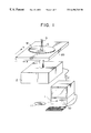
- FIG. 1 is a schematic perspective view of an etching apparatus for working the wafer flattening process of the present invention
- FIG. 2 is a plan view for explaining position-thickness data of a wafer
- FIG. 3 is a plan view for explaining position-speed data
- FIG. 4 is a graph of the relationship between the nozzle relative speed and the value of thickness of the wafer
- FIG. 5 is a plan view of the method of determination of the position-speed data inside a predetermined area
- FIG. 6 is a plan view of the state of scanning by the nozzle
- FIG. 7 is a plan view for explaining an etching operation of the outer rim of the wafer.
- FIG. 8 is a sectional view taken along the line A—A of FIG. 7;
- FIG. 9 is a schematic sectional view of an example of a wafer flattening process of the related art.
- FIG. 10 is a view of the state of spraying of activated species gas from a nozzle
- FIG. 11 is a schematic view for explaining a flattening operation by superposition of activated species gas.
- FIG. 12 is a schematic sectional view for explaining a problem in the wafer flattening process of the related art.
- FIG. 1 is a schematic perspective view of an etching apparatus for working the wafer flattening process of the present invention.
- the etching apparatus is provided with a computer 1 , an X-Y drive mechanism 2 for making a stage 20 mounting a wafer W move horizontally under control of the computer 1 , and a nozzle 3 .
- the computer 1 is provided with a CD-ROM drive 10 for driving a CD-ROM 11 serving as a storage medium and functions to output a control signal C to the X-Y drive mechanism 2 based on the position-speed data D in the CD-ROM 11 .
- the X-Y drive mechanism 2 is a mechanism for making the stage 20 move to a predetermined position at a predetermined speed based on the control signal C from the computer 1 . That is, the X-Y drive mechanism 2 makes the nozzle 3 scan the wafer W at predetermined relative positions at a predetermined relative speed.
- the nozzle 3 sprays activated species gas G generated by a not shown plasma generator toward the wafer W and is affixed at a predetermined location above the wafer W.
- the portion of the etching radius r of the wafer W positioned directly under the nozzle 3 is etched by the activated species gas G from the nozzle 3 .
- FIG. 2 is a plan view for explaining position-thickness data D′ of a wafer W
- FIG. 3 is a plan view for explaining position-speed data D
- FIG. 4 is a graph of the relationship between the relative speed of the nozzle 3 and the value of thickness of the wafer W. Note that in FIG. 2 and FIG. 3, the squares of the graph are drawn larger to facilitate understanding.
- the plane including the wafer W is divided into squares of about 1 mm to 2 mm size to form the X-Y coordinate system.
- the position-thickness data D′ is comprised of the X-Y coordinates (x,y) of each point and the value of thickness T of the wafer W at each point.
- the position-speed data D is comprised of the data D(x,y,V) where the value of thickness T in the position-thickness data D′ (x,y,T) is converted to a relative speed V of the nozzle 3 inversely proportional to the value of thickness T by a not shown converter.
- the relative speed is not made the high speed Vmax uniformly such as with the position-speed data D 3 , but the relative speed is converted to correspond to the position-speed data D in the wafer W and at a point near the outer rim Wc.
- FIG. 5 is a plan view of the method of determination of the position-speed data D inside the area S.
- the position-speed data D 4 at that point P 4 is (x 4 ,y 4 ,V 4 ) and the relative speed V 4 is not Vmax.
- the imaginary line L extending from the center of the wafer W in the radial direction and passing through the point P 4 is assumed and the relative speeds of the position-speed data D of the points P 4 - 1 to P 4 - 3 closest to the imaginary line L are all made the same as the relative speed V 4 of the position-speed data D 4 .
- the relative speeds of the position-speed data D of the points P 5 - 1 to P 5 - 3 closest to the imaginary line L′ passing through that point are made the same as the high speed Vmax of the position-speed data D 5 .
- the relative speed of the position-speed data D of a point near the outer rim Wc is copied to the position-speed data D of the points outside the outer rim Wc in the area S to set so-called dummy data for the area.
- FIG. 6 is a plan view of the state of scanning by the nozzle 3 .
- the computer 1 when the CD-ROM 11 is inserted into the CD-ROM drive 10 of the computer 1 , the computer 1 reads the position-speed data D and outputs a control signal C corresponding to the position-speed data D of the different points to the X-Y drive mechanism 2 .
- the X-Y drive mechanism 2 makes the stage 20 move in the X-Y direction based on the control signal C and, as shown in FIG. 6, the nozzle 3 scans the X-Y plane in a zigzag manner.
- the nozzle relative speed at the position-speed data D of the different points outside of the area S is the high speed Vmax, so the nozzle 3 enters a state moving at the high speed Vmax outside of the area S.
- the relative speed V of the position-speed data D is set corresponding to the values of thickness T of the different points, so when passing over a relatively thick portion, the nozzle 3 moves slower corresponding to the thickness of the relatively thick portion, while when passing over a portion not a relatively thick portion, the nozzle 3 moves at the high speed Vmax.
- the nozzle relative speed of the position-speed data D of the different points in the area S closest to the imaginary line L passing through the points near the outer rim Wc is set to be the same as the nozzle relative speed of the position-speed data D of the points near the outer rim Wc and the position-speed data of the points is used as the dummy data, so the outer rim is subject to the effects of the activated species gas G of the nozzle 3 .
- the nozzle relative speed of the dummy data D of the points P 4 - 1 to P 4 - 3 corresponding to the point P 4 of the relatively thick portion Wa is the “V4”of the position-speed data D of the point P 4 . Therefore, the nozzle 3 passes over the points P 4 - 1 to P 4 - 3 , the point P 4 , and the point P 6 by the nozzle relative speed V 4 .
- the relatively thick portion Wa of the point P 4 is etched like by the effect of superposition of the activated species gas G of the nozzle 3 approaching along the imaginary line L at the relative speed V 4 and the activated species gas G from the nozzle 3 passing through the point P 4 and reaching the point P 6 at the same speed. Therefore, the relatively thick portion Wa of the point P 4 is etched in the same way as the relatively thick portion in the wafer W and similarly flattened.
- the nozzle relative speed of the dummy data D of the points P 5 - 1 to P 5 - 3 near the imaginary line L′ is set to the high speed Vmax, so the nozzle 3 approaches the point P 5 along the imaginary line L′ at the speed Vmax, then passes through it at the same speed, whereby etching is performed in the same way as at portions inside the wafer W not relatively thick portions.
- a CD-ROM was used as the storage medium for storing the position-speed data D, but of course it is also possible to store the position-speed data D in various other types of storage media such as floppy disks, minidiscs, digital video disks, hard disks, etc.
- the explanation was made of a process for flattening the entire surface of the wafer W, but it is sufficient to flatten just the flatness quality area inside the wafer W to a high precision in some cases.
- an area S extending from the outer rim of the flatness quality area by exactly the etching radius r is set and the nozzle relative speed of the position-speed data D in that area S is made the same as the nozzle relative speed of the position-speed data D of the outer rim in the same way as the above embodiment so as to flatten the entire flatness quality area to a high precision.
- the nozzle relative speed of the position-speed data D of the points closest to the imaginary line L inside the area S was made the same as the nozzle relative speed of the position-speed data D of the wafer outer rim, the invention is not limited to within the area S. It is also possible to make the nozzle relative speed of the position-speed data D of all points closest to the imaginary line L outside of the outer rim Wc the same as the nozzle relative speed of the position-speed data D of the outer rim.
- the outer rim of a predetermined area is subject to effects like that of activated species gas from a nozzle heading from the outside along an imaginary line at a nozzle relative speed set for that outer rim, so there is the advantageous effect that the outer rim can be flattened in the same way as the inside of the predetermined area.
- the nozzle relative speed becomes substantially the same as the nozzle relative speed set for the predetermined area only when the nozzle located at the outside of the predetermined area moves within a distance of about half of the etching diameter of the activated species gas from the outer rim of the predetermined area.
Abstract
Description
Claims (8)
Applications Claiming Priority (2)
| Application Number | Priority Date | Filing Date | Title |
|---|---|---|---|
| JP07668098A JP3871433B2 (en) | 1998-03-10 | 1998-03-10 | Wafer planarization method and recording medium |
| JP10-076680 | 1998-03-10 |
Publications (1)
| Publication Number | Publication Date |
|---|---|
| US6496748B1 true US6496748B1 (en) | 2002-12-17 |
Family
ID=13612156
Family Applications (1)
| Application Number | Title | Priority Date | Filing Date |
|---|---|---|---|
| US09/234,937 Expired - Fee Related US6496748B1 (en) | 1998-03-10 | 1999-01-21 | Wafer flattening process and storage medium |
Country Status (2)
| Country | Link |
|---|---|
| US (1) | US6496748B1 (en) |
| JP (1) | JP3871433B2 (en) |
Cited By (1)
| Publication number | Priority date | Publication date | Assignee | Title |
|---|---|---|---|---|
| US20030199168A1 (en) * | 2002-04-22 | 2003-10-23 | Speedfam Co., Ltd. | Local dry etching method |
Families Citing this family (1)
| Publication number | Priority date | Publication date | Assignee | Title |
|---|---|---|---|---|
| US6451217B1 (en) * | 1998-06-09 | 2002-09-17 | Speedfam-Ipec Co., Ltd. | Wafer etching method |
Citations (5)
| Publication number | Priority date | Publication date | Assignee | Title |
|---|---|---|---|---|
| JPH0927482A (en) | 1995-07-11 | 1997-01-28 | Speedfam Co Ltd | Plasma etching apparatus |
| US6254718B1 (en) * | 1998-04-21 | 2001-07-03 | Speedfam Co., Ltd. | Combined CMP and plasma etching wafer flattening system |
| US6280645B1 (en) * | 1998-07-21 | 2001-08-28 | Yasuhiro Horiike And Speedfam Co, Ltd. | Wafer flattening process and system |
| US6303511B2 (en) * | 1999-02-12 | 2001-10-16 | Speedfam-Ipec Co., Ltd. | Wafer flattening process |
| US6360687B1 (en) * | 1998-11-26 | 2002-03-26 | Speedfam-Ipec Co., Ltd | Wafer flattening system |
-
1998
- 1998-03-10 JP JP07668098A patent/JP3871433B2/en not_active Expired - Lifetime
-
1999
- 1999-01-21 US US09/234,937 patent/US6496748B1/en not_active Expired - Fee Related
Patent Citations (5)
| Publication number | Priority date | Publication date | Assignee | Title |
|---|---|---|---|---|
| JPH0927482A (en) | 1995-07-11 | 1997-01-28 | Speedfam Co Ltd | Plasma etching apparatus |
| US6254718B1 (en) * | 1998-04-21 | 2001-07-03 | Speedfam Co., Ltd. | Combined CMP and plasma etching wafer flattening system |
| US6280645B1 (en) * | 1998-07-21 | 2001-08-28 | Yasuhiro Horiike And Speedfam Co, Ltd. | Wafer flattening process and system |
| US6360687B1 (en) * | 1998-11-26 | 2002-03-26 | Speedfam-Ipec Co., Ltd | Wafer flattening system |
| US6303511B2 (en) * | 1999-02-12 | 2001-10-16 | Speedfam-Ipec Co., Ltd. | Wafer flattening process |
Cited By (2)
| Publication number | Priority date | Publication date | Assignee | Title |
|---|---|---|---|---|
| US20030199168A1 (en) * | 2002-04-22 | 2003-10-23 | Speedfam Co., Ltd. | Local dry etching method |
| US6908566B2 (en) | 2002-04-22 | 2005-06-21 | Speedfam Co., Ltd. | Local dry etching method |
Also Published As
| Publication number | Publication date |
|---|---|
| JP3871433B2 (en) | 2007-01-24 |
| JPH11260806A (en) | 1999-09-24 |
Similar Documents
| Publication | Publication Date | Title |
|---|---|---|
| JP3612158B2 (en) | Plasma etching method and apparatus | |
| US5086015A (en) | Method of etching a semiconductor device by an ion beam | |
| CN100383859C (en) | Production process and production device of magnetic recording medium | |
| JP2000509181A (en) | Thin film magnetic recording head and system and method for manufacturing the same | |
| US6667242B2 (en) | Brim and gas escape for non-contact wafer holder | |
| TWI646598B (en) | Microscopic three-dimensional structure forming method and microscopic three-dimensional structure | |
| US6496748B1 (en) | Wafer flattening process and storage medium | |
| JPH0653178A (en) | Apparatus and method for optimum scanning of two-dimensional surface of one or more objects | |
| JP2934153B2 (en) | Photoresist film forming method | |
| JPH01298585A (en) | Slider for magnetic head and its forming method | |
| JPH10321507A (en) | Electron beam exposure method | |
| KR100264191B1 (en) | Charged particle beam writing method and apparatus therefor | |
| JP2002252210A (en) | Local etching method | |
| US7025514B2 (en) | Development apparatus for manufacturing semiconductor device | |
| JPH0857382A (en) | Device for detecting liquid-coating nozzle height and method for controlling nozzle height using the same | |
| JPH04309213A (en) | Charger particle beam lithography method | |
| KR20210072690A (en) | A semiconductor wafer dicing process | |
| JPH07205028A (en) | Processing method and device for fine particle injection | |
| JP2000141344A (en) | Method and device for working brake-groove | |
| JPH0697084A (en) | Beam induction process apparatus | |
| JPH0581614A (en) | Thin-film magnetic head and production thereof | |
| JPH06295857A (en) | Trapezoidal pattern writing method | |
| JPH01183846A (en) | Large-sized substrate with which plurality of solid-state image sensing devices are integrated | |
| JPH06150600A (en) | Floating type magnetic head | |
| JPH03257925A (en) | Forming method of wiring pattern |
Legal Events
| Date | Code | Title | Description |
|---|---|---|---|
| AS | Assignment |
Owner name: YASUHIRO HORIIKE, JAPAN Free format text: ASSIGNMENT OF ASSIGNORS INTEREST;ASSIGNORS:YANAGISAWA, MICHIHIKO;IIDA, SHINYA;HORIIKE, YASUHIRO;REEL/FRAME:009819/0994 Effective date: 19990301 Owner name: SPEEDFAM CO.,LTD., JAPAN Free format text: ASSIGNMENT OF ASSIGNORS INTEREST;ASSIGNORS:YANAGISAWA, MICHIHIKO;IIDA, SHINYA;HORIIKE, YASUHIRO;REEL/FRAME:009819/0994 Effective date: 19990301 |
|
| FEPP | Fee payment procedure |
Free format text: PAYOR NUMBER ASSIGNED (ORIGINAL EVENT CODE: ASPN); ENTITY STATUS OF PATENT OWNER: SMALL ENTITY Free format text: PAYER NUMBER DE-ASSIGNED (ORIGINAL EVENT CODE: RMPN); ENTITY STATUS OF PATENT OWNER: SMALL ENTITY |
|
| FEPP | Fee payment procedure |
Free format text: PAT HOLDER CLAIMS SMALL ENTITY STATUS, ENTITY STATUS SET TO SMALL (ORIGINAL EVENT CODE: LTOS); ENTITY STATUS OF PATENT OWNER: SMALL ENTITY |
|
| FPAY | Fee payment |
Year of fee payment: 4 |
|
| REMI | Maintenance fee reminder mailed | ||
| LAPS | Lapse for failure to pay maintenance fees | ||
| STCH | Information on status: patent discontinuation |
Free format text: PATENT EXPIRED DUE TO NONPAYMENT OF MAINTENANCE FEES UNDER 37 CFR 1.362 |
|
| FP | Lapsed due to failure to pay maintenance fee |
Effective date: 20101217 |