US6492484B2 - Polycarbodiimide - Google Patents
Polycarbodiimide Download PDFInfo
- Publication number
- US6492484B2 US6492484B2 US09/941,559 US94155901A US6492484B2 US 6492484 B2 US6492484 B2 US 6492484B2 US 94155901 A US94155901 A US 94155901A US 6492484 B2 US6492484 B2 US 6492484B2
- Authority
- US
- United States
- Prior art keywords
- polycarbodiimide
- group
- adhesive film
- formula
- carbon atoms
- Prior art date
- Legal status (The legal status is an assumption and is not a legal conclusion. Google has not performed a legal analysis and makes no representation as to the accuracy of the status listed.)
- Expired - Fee Related
Links
- 239000002313 adhesive film Substances 0.000 claims abstract description 137
- 239000004065 semiconductor Substances 0.000 claims abstract description 114
- 125000004432 carbon atom Chemical group C* 0.000 claims abstract description 36
- 125000003118 aryl group Chemical group 0.000 claims abstract description 22
- 125000002947 alkylene group Chemical group 0.000 claims abstract description 17
- 238000004519 manufacturing process Methods 0.000 claims abstract description 8
- 239000000758 substrate Substances 0.000 claims description 35
- 150000002009 diols Chemical class 0.000 claims description 23
- 239000003054 catalyst Substances 0.000 claims description 16
- 229920000515 polycarbonate Polymers 0.000 claims description 16
- 239000004417 polycarbonate Substances 0.000 claims description 16
- 125000000217 alkyl group Chemical group 0.000 claims description 14
- IQPQWNKOIGAROB-UHFFFAOYSA-N isocyanate group Chemical group [N-]=C=O IQPQWNKOIGAROB-UHFFFAOYSA-N 0.000 claims description 14
- 229920002635 polyurethane Polymers 0.000 claims description 11
- 239000004814 polyurethane Substances 0.000 claims description 11
- 125000003545 alkoxy group Chemical group 0.000 claims description 6
- 125000004836 hexamethylene group Chemical group [H]C([H])([*:2])C([H])([H])C([H])([H])C([H])([H])C([H])([H])C([H])([H])[*:1] 0.000 claims description 6
- 125000005843 halogen group Chemical group 0.000 claims description 5
- 125000004435 hydrogen atom Chemical group [H]* 0.000 claims description 4
- 125000004430 oxygen atom Chemical group O* 0.000 claims description 4
- 239000000243 solution Substances 0.000 description 54
- 238000006243 chemical reaction Methods 0.000 description 50
- 239000000853 adhesive Substances 0.000 description 34
- 230000001070 adhesive effect Effects 0.000 description 34
- 238000000034 method Methods 0.000 description 25
- 238000010438 heat treatment Methods 0.000 description 24
- 230000000052 comparative effect Effects 0.000 description 22
- 0 [3*]N=C=N[2*]N=C=N[2*]N([H])C(=O)OCCCC[1*]OC(=O)O[1*]OC(=O)N([H])[2*]CCCCN=C=N[2*]N=C=N[3*] Chemical compound [3*]N=C=N[2*]N=C=N[2*]N([H])C(=O)OCCCC[1*]OC(=O)O[1*]OC(=O)N([H])[2*]CCCCN=C=N[2*]N=C=N[3*] 0.000 description 17
- 239000000047 product Substances 0.000 description 17
- 239000000956 alloy Substances 0.000 description 13
- 229910045601 alloy Inorganic materials 0.000 description 13
- 238000000576 coating method Methods 0.000 description 12
- JHIVVAPYMSGYDF-UHFFFAOYSA-N cyclohexanone Chemical compound O=C1CCCCC1 JHIVVAPYMSGYDF-UHFFFAOYSA-N 0.000 description 12
- 239000002904 solvent Substances 0.000 description 12
- 239000013585 weight reducing agent Substances 0.000 description 12
- 238000010521 absorption reaction Methods 0.000 description 11
- 239000011248 coating agent Substances 0.000 description 11
- -1 ethylene, tetramethylene, hexamethylene, octamethylene Chemical group 0.000 description 11
- 230000008569 process Effects 0.000 description 11
- 229920005989 resin Polymers 0.000 description 11
- 239000011347 resin Substances 0.000 description 11
- DVKJHBMWWAPEIU-UHFFFAOYSA-N toluene 2,4-diisocyanate Chemical compound CC1=CC=C(N=C=O)C=C1N=C=O DVKJHBMWWAPEIU-UHFFFAOYSA-N 0.000 description 9
- PJVRNNRZWASOIT-UHFFFAOYSA-N 1-isocyanato-4-propan-2-ylbenzene Chemical compound CC(C)C1=CC=C(N=C=O)C=C1 PJVRNNRZWASOIT-UHFFFAOYSA-N 0.000 description 8
- RYGMFSIKBFXOCR-UHFFFAOYSA-N Copper Chemical compound [Cu] RYGMFSIKBFXOCR-UHFFFAOYSA-N 0.000 description 8
- 238000002329 infrared spectrum Methods 0.000 description 8
- 239000011133 lead Substances 0.000 description 8
- 229910052751 metal Inorganic materials 0.000 description 8
- 239000002184 metal Substances 0.000 description 8
- 238000012360 testing method Methods 0.000 description 8
- YMKWWHFRGALXLE-UHFFFAOYSA-N 4-methyl-1-phenyl-2,3-dihydro-1$l^{5}-phosphole 1-oxide Chemical compound C1CC(C)=CP1(=O)C1=CC=CC=C1 YMKWWHFRGALXLE-UHFFFAOYSA-N 0.000 description 7
- XUIMIQQOPSSXEZ-UHFFFAOYSA-N Silicon Chemical compound [Si] XUIMIQQOPSSXEZ-UHFFFAOYSA-N 0.000 description 7
- 230000008034 disappearance Effects 0.000 description 7
- 230000009477 glass transition Effects 0.000 description 7
- 239000010410 layer Substances 0.000 description 7
- 238000003825 pressing Methods 0.000 description 7
- 238000007789 sealing Methods 0.000 description 7
- 239000000126 substance Substances 0.000 description 7
- PXHVJJICTQNCMI-UHFFFAOYSA-N Nickel Chemical compound [Ni] PXHVJJICTQNCMI-UHFFFAOYSA-N 0.000 description 6
- CTQNGGLPUBDAKN-UHFFFAOYSA-N O-Xylene Chemical compound CC1=CC=CC=C1C CTQNGGLPUBDAKN-UHFFFAOYSA-N 0.000 description 6
- 239000012790 adhesive layer Substances 0.000 description 6
- VPKDCDLSJZCGKE-UHFFFAOYSA-N carbodiimide group Chemical group N=C=N VPKDCDLSJZCGKE-UHFFFAOYSA-N 0.000 description 6
- 239000011889 copper foil Substances 0.000 description 6
- 239000011888 foil Substances 0.000 description 6
- 239000003960 organic solvent Substances 0.000 description 6
- 238000002360 preparation method Methods 0.000 description 6
- 238000010008 shearing Methods 0.000 description 6
- 239000010703 silicon Substances 0.000 description 6
- 229910052710 silicon Inorganic materials 0.000 description 6
- 239000008096 xylene Substances 0.000 description 6
- RTTZISZSHSCFRH-UHFFFAOYSA-N 1,3-bis(isocyanatomethyl)benzene Chemical compound O=C=NCC1=CC=CC(CN=C=O)=C1 RTTZISZSHSCFRH-UHFFFAOYSA-N 0.000 description 5
- 125000002887 hydroxy group Chemical group [H]O* 0.000 description 5
- 239000000203 mixture Substances 0.000 description 5
- 230000000704 physical effect Effects 0.000 description 5
- 238000010992 reflux Methods 0.000 description 5
- GWHJZXXIDMPWGX-UHFFFAOYSA-N CC1=CC(C)=C(C)C=C1 Chemical compound CC1=CC(C)=C(C)C=C1 GWHJZXXIDMPWGX-UHFFFAOYSA-N 0.000 description 4
- OKTJSMMVPCPJKN-UHFFFAOYSA-N Carbon Chemical compound [C] OKTJSMMVPCPJKN-UHFFFAOYSA-N 0.000 description 4
- KDLHZDBZIXYQEI-UHFFFAOYSA-N Palladium Chemical compound [Pd] KDLHZDBZIXYQEI-UHFFFAOYSA-N 0.000 description 4
- ATUOYWHBWRKTHZ-UHFFFAOYSA-N Propane Chemical compound CCC ATUOYWHBWRKTHZ-UHFFFAOYSA-N 0.000 description 4
- WYURNTSHIVDZCO-UHFFFAOYSA-N Tetrahydrofuran Chemical compound C1CCOC1 WYURNTSHIVDZCO-UHFFFAOYSA-N 0.000 description 4
- 239000012298 atmosphere Substances 0.000 description 4
- 239000000463 material Substances 0.000 description 4
- 239000003223 protective agent Substances 0.000 description 4
- 229920001187 thermosetting polymer Polymers 0.000 description 4
- ZWEHNKRNPOVVGH-UHFFFAOYSA-N 2-Butanone Chemical compound CCC(C)=O ZWEHNKRNPOVVGH-UHFFFAOYSA-N 0.000 description 3
- UPMLOUAZCHDJJD-UHFFFAOYSA-N 4,4'-Diphenylmethane Diisocyanate Chemical compound C1=CC(N=C=O)=CC=C1CC1=CC=C(N=C=O)C=C1 UPMLOUAZCHDJJD-UHFFFAOYSA-N 0.000 description 3
- CSCPPACGZOOCGX-UHFFFAOYSA-N Acetone Chemical compound CC(C)=O CSCPPACGZOOCGX-UHFFFAOYSA-N 0.000 description 3
- URLKBWYHVLBVBO-UHFFFAOYSA-N CC1=CC=C(C)C=C1 Chemical compound CC1=CC=C(C)C=C1 URLKBWYHVLBVBO-UHFFFAOYSA-N 0.000 description 3
- FYGHSUNMUKGBRK-UHFFFAOYSA-N CC1=CC=CC(C)=C1C Chemical compound CC1=CC=CC(C)=C1C FYGHSUNMUKGBRK-UHFFFAOYSA-N 0.000 description 3
- LFQSCWFLJHTTHZ-UHFFFAOYSA-N Ethanol Chemical compound CCO LFQSCWFLJHTTHZ-UHFFFAOYSA-N 0.000 description 3
- KFZMGEQAYNKOFK-UHFFFAOYSA-N Isopropanol Chemical compound CC(C)O KFZMGEQAYNKOFK-UHFFFAOYSA-N 0.000 description 3
- OKKJLVBELUTLKV-UHFFFAOYSA-N Methanol Chemical compound OC OKKJLVBELUTLKV-UHFFFAOYSA-N 0.000 description 3
- VYPSYNLAJGMNEJ-UHFFFAOYSA-N Silicium dioxide Chemical compound O=[Si]=O VYPSYNLAJGMNEJ-UHFFFAOYSA-N 0.000 description 3
- BQCADISMDOOEFD-UHFFFAOYSA-N Silver Chemical compound [Ag] BQCADISMDOOEFD-UHFFFAOYSA-N 0.000 description 3
- YXFVVABEGXRONW-UHFFFAOYSA-N Toluene Chemical compound CC1=CC=CC=C1 YXFVVABEGXRONW-UHFFFAOYSA-N 0.000 description 3
- 239000000654 additive Substances 0.000 description 3
- 239000003463 adsorbent Substances 0.000 description 3
- 239000003795 chemical substances by application Substances 0.000 description 3
- 229910052731 fluorine Inorganic materials 0.000 description 3
- 239000007788 liquid Substances 0.000 description 3
- 125000002496 methyl group Chemical group [H]C([H])([H])* 0.000 description 3
- 239000000178 monomer Substances 0.000 description 3
- 229910052759 nickel Inorganic materials 0.000 description 3
- 239000000843 powder Substances 0.000 description 3
- 230000035484 reaction time Effects 0.000 description 3
- 229910052709 silver Inorganic materials 0.000 description 3
- 239000004332 silver Substances 0.000 description 3
- 238000003860 storage Methods 0.000 description 3
- XKRFYHLGVUSROY-UHFFFAOYSA-N Argon Chemical compound [Ar] XKRFYHLGVUSROY-UHFFFAOYSA-N 0.000 description 2
- IJGRMHOSHXDMSA-UHFFFAOYSA-N Atomic nitrogen Chemical compound N#N IJGRMHOSHXDMSA-UHFFFAOYSA-N 0.000 description 2
- QBXQLUVRTKMWIL-UHFFFAOYSA-N C1=CC=CC=C1.C1=CC=CC=C1.CC.CC.CCC Chemical compound C1=CC=CC=C1.C1=CC=CC=C1.CC.CC.CCC QBXQLUVRTKMWIL-UHFFFAOYSA-N 0.000 description 2
- LCEXZXRIBXVGJD-UHFFFAOYSA-N C1=CC=CC=C1.CC.CC(C)C Chemical compound C1=CC=CC=C1.CC.CC(C)C LCEXZXRIBXVGJD-UHFFFAOYSA-N 0.000 description 2
- YPAFXRXQIDJINC-UHFFFAOYSA-N CC.CC.CC1=CC=CC=C1 Chemical compound CC.CC.CC1=CC=CC=C1 YPAFXRXQIDJINC-UHFFFAOYSA-N 0.000 description 2
- HEDRZPFGACZZDS-UHFFFAOYSA-N Chloroform Chemical compound ClC(Cl)Cl HEDRZPFGACZZDS-UHFFFAOYSA-N 0.000 description 2
- VYZAMTAEIAYCRO-UHFFFAOYSA-N Chromium Chemical compound [Cr] VYZAMTAEIAYCRO-UHFFFAOYSA-N 0.000 description 2
- XEEYBQQBJWHFJM-UHFFFAOYSA-N Iron Chemical compound [Fe] XEEYBQQBJWHFJM-UHFFFAOYSA-N 0.000 description 2
- CPLXHLVBOLITMK-UHFFFAOYSA-N Magnesium oxide Chemical compound [Mg]=O CPLXHLVBOLITMK-UHFFFAOYSA-N 0.000 description 2
- OFBQJSOFQDEBGM-UHFFFAOYSA-N Pentane Chemical compound CCCCC OFBQJSOFQDEBGM-UHFFFAOYSA-N 0.000 description 2
- 229910052581 Si3N4 Inorganic materials 0.000 description 2
- ATJFFYVFTNAWJD-UHFFFAOYSA-N Tin Chemical compound [Sn] ATJFFYVFTNAWJD-UHFFFAOYSA-N 0.000 description 2
- HCHKCACWOHOZIP-UHFFFAOYSA-N Zinc Chemical compound [Zn] HCHKCACWOHOZIP-UHFFFAOYSA-N 0.000 description 2
- 238000002835 absorbance Methods 0.000 description 2
- 238000000862 absorption spectrum Methods 0.000 description 2
- 230000000996 additive effect Effects 0.000 description 2
- 229910052782 aluminium Inorganic materials 0.000 description 2
- XAGFODPZIPBFFR-UHFFFAOYSA-N aluminium Chemical compound [Al] XAGFODPZIPBFFR-UHFFFAOYSA-N 0.000 description 2
- PNEYBMLMFCGWSK-UHFFFAOYSA-N aluminium oxide Inorganic materials [O-2].[O-2].[O-2].[Al+3].[Al+3] PNEYBMLMFCGWSK-UHFFFAOYSA-N 0.000 description 2
- 229910052799 carbon Inorganic materials 0.000 description 2
- 229910052804 chromium Inorganic materials 0.000 description 2
- 239000011651 chromium Substances 0.000 description 2
- 229910052802 copper Inorganic materials 0.000 description 2
- 239000010949 copper Substances 0.000 description 2
- 238000005520 cutting process Methods 0.000 description 2
- 229910001873 dinitrogen Inorganic materials 0.000 description 2
- 239000003822 epoxy resin Substances 0.000 description 2
- 238000011049 filling Methods 0.000 description 2
- 125000001153 fluoro group Chemical group F* 0.000 description 2
- 239000007789 gas Substances 0.000 description 2
- PCHJSUWPFVWCPO-UHFFFAOYSA-N gold Chemical compound [Au] PCHJSUWPFVWCPO-UHFFFAOYSA-N 0.000 description 2
- 229910052737 gold Inorganic materials 0.000 description 2
- 239000010931 gold Substances 0.000 description 2
- 230000006872 improvement Effects 0.000 description 2
- 230000000977 initiatory effect Effects 0.000 description 2
- 125000000956 methoxy group Chemical group [H]C([H])([H])O* 0.000 description 2
- VLKZOEOYAKHREP-UHFFFAOYSA-N n-Hexane Chemical compound CCCCCC VLKZOEOYAKHREP-UHFFFAOYSA-N 0.000 description 2
- 229910052763 palladium Inorganic materials 0.000 description 2
- 125000001997 phenyl group Chemical group [H]C1=C([H])C([H])=C(*)C([H])=C1[H] 0.000 description 2
- 229920000647 polyepoxide Polymers 0.000 description 2
- 229920000139 polyethylene terephthalate Polymers 0.000 description 2
- 239000005020 polyethylene terephthalate Substances 0.000 description 2
- 229920001721 polyimide Polymers 0.000 description 2
- 229920001296 polysiloxane Polymers 0.000 description 2
- 239000001294 propane Substances 0.000 description 2
- HQVNEWCFYHHQES-UHFFFAOYSA-N silicon nitride Chemical compound N12[Si]34N5[Si]62N3[Si]51N64 HQVNEWCFYHHQES-UHFFFAOYSA-N 0.000 description 2
- 229910000679 solder Inorganic materials 0.000 description 2
- YLQBMQCUIZJEEH-UHFFFAOYSA-N tetrahydrofuran Natural products C=1C=COC=1 YLQBMQCUIZJEEH-UHFFFAOYSA-N 0.000 description 2
- 238000005979 thermal decomposition reaction Methods 0.000 description 2
- 239000011135 tin Substances 0.000 description 2
- 229910052718 tin Inorganic materials 0.000 description 2
- 238000002525 ultrasonication Methods 0.000 description 2
- 229910052725 zinc Inorganic materials 0.000 description 2
- 239000011701 zinc Substances 0.000 description 2
- WSLDOOZREJYCGB-UHFFFAOYSA-N 1,2-Dichloroethane Chemical compound ClCCCl WSLDOOZREJYCGB-UHFFFAOYSA-N 0.000 description 1
- RYHBNJHYFVUHQT-UHFFFAOYSA-N 1,4-Dioxane Chemical compound C1COCCO1 RYHBNJHYFVUHQT-UHFFFAOYSA-N 0.000 description 1
- IOSIDVPNBKUUFA-UHFFFAOYSA-N 1-ethyl-2,3-dihydro-1$l^{5}-phosphole 1-oxide Chemical compound CCP1(=O)CCC=C1 IOSIDVPNBKUUFA-UHFFFAOYSA-N 0.000 description 1
- UYZREAQIFNECFH-UHFFFAOYSA-N 1-isocyanato-3-(2-methylphenyl)benzene Chemical compound CC1=CC=CC=C1C1=CC=CC(N=C=O)=C1 UYZREAQIFNECFH-UHFFFAOYSA-N 0.000 description 1
- URJPTWVOOWGKTB-UHFFFAOYSA-N 1-isocyanato-4-(2-methylphenyl)benzene Chemical compound CC1=CC=CC=C1C1=CC=C(N=C=O)C=C1 URJPTWVOOWGKTB-UHFFFAOYSA-N 0.000 description 1
- GFNKTLQTQSALEJ-UHFFFAOYSA-N 1-isocyanato-4-nitrobenzene Chemical compound [O-][N+](=O)C1=CC=C(N=C=O)C=C1 GFNKTLQTQSALEJ-UHFFFAOYSA-N 0.000 description 1
- YUQUHJGNZFFDAA-UHFFFAOYSA-N 1-phenyl-2,3-dihydro-1$l^{5}-phosphole 1-oxide Chemical compound C=1C=CC=CC=1P1(=O)CCC=C1 YUQUHJGNZFFDAA-UHFFFAOYSA-N 0.000 description 1
- 125000004825 2,2-dimethylpropylene group Chemical group [H]C([H])([H])C(C([H])([H])[H])(C([H])([H])[*:1])C([H])([H])[*:2] 0.000 description 1
- JXGNHEUFHNJWDY-UHFFFAOYSA-N 2,5-dihydro-1h-phosphole Chemical class C1PCC=C1 JXGNHEUFHNJWDY-UHFFFAOYSA-N 0.000 description 1
- PUINVXGYZJXMMX-UHFFFAOYSA-N 4-isocyanatobenzaldehyde Chemical compound O=CC1=CC=C(N=C=O)C=C1 PUINVXGYZJXMMX-UHFFFAOYSA-N 0.000 description 1
- ZCYVEMRRCGMTRW-UHFFFAOYSA-N 7553-56-2 Chemical group [I] ZCYVEMRRCGMTRW-UHFFFAOYSA-N 0.000 description 1
- WKBOTKDWSSQWDR-UHFFFAOYSA-N Bromine atom Chemical group [Br] WKBOTKDWSSQWDR-UHFFFAOYSA-N 0.000 description 1
- MVKVAJLKRARYJN-UHFFFAOYSA-N C1=CC=C(CC2=CC=CC=C2)C=C1.C1=CC=C(CC2=CC=CC=C2)C=C1.C1=CC=C(OC2=CC=CC=C2)C=C1.C1=CC=C(OC2=CC=CC=C2)C=C1.C1=CC=CC=C1.C1=CC=CC=C1.CC.CC.CC.CC.CC.CC.CC.CC.CC.CC.CC.CC.CC.CC.CC.CC1=CC=C(OC2=CC=C(C(C)(C)C3=CC=C(OC4=CC=C(C)C=C4)C=C3)C=C2)C=C1.CC1=CC=C(OC2=CC=C(C(C3=CC=C(OC4=CC=C(C)C=C4)C=C3)(C(F)(F)F)C(F)(F)F)C=C2)C=C1.CC1=CC=C(OCC(C)(C)COC2=CC=C(C)C=C2)C=C1.CC1=CC=C(OCCCCCOC2=CC=C(C)C=C2)C=C1.COC.COC.COC Chemical compound C1=CC=C(CC2=CC=CC=C2)C=C1.C1=CC=C(CC2=CC=CC=C2)C=C1.C1=CC=C(OC2=CC=CC=C2)C=C1.C1=CC=C(OC2=CC=CC=C2)C=C1.C1=CC=CC=C1.C1=CC=CC=C1.CC.CC.CC.CC.CC.CC.CC.CC.CC.CC.CC.CC.CC.CC.CC.CC1=CC=C(OC2=CC=C(C(C)(C)C3=CC=C(OC4=CC=C(C)C=C4)C=C3)C=C2)C=C1.CC1=CC=C(OC2=CC=C(C(C3=CC=C(OC4=CC=C(C)C=C4)C=C3)(C(F)(F)F)C(F)(F)F)C=C2)C=C1.CC1=CC=C(OCC(C)(C)COC2=CC=C(C)C=C2)C=C1.CC1=CC=C(OCCCCCOC2=CC=C(C)C=C2)C=C1.COC.COC.COC MVKVAJLKRARYJN-UHFFFAOYSA-N 0.000 description 1
- STUPVELWKGXMQS-UHFFFAOYSA-N CC1=CP(=O)CC1 Chemical compound CC1=CP(=O)CC1 STUPVELWKGXMQS-UHFFFAOYSA-N 0.000 description 1
- LYCAIKOWRPUZTN-UHFFFAOYSA-N Ethylene glycol Chemical compound OCCO LYCAIKOWRPUZTN-UHFFFAOYSA-N 0.000 description 1
- YCKRFDGAMUMZLT-UHFFFAOYSA-N Fluorine atom Chemical compound [F] YCKRFDGAMUMZLT-UHFFFAOYSA-N 0.000 description 1
- NTIZESTWPVYFNL-UHFFFAOYSA-N Methyl isobutyl ketone Chemical compound CC(C)CC(C)=O NTIZESTWPVYFNL-UHFFFAOYSA-N 0.000 description 1
- UIHCLUNTQKBZGK-UHFFFAOYSA-N Methyl isobutyl ketone Natural products CCC(C)C(C)=O UIHCLUNTQKBZGK-UHFFFAOYSA-N 0.000 description 1
- ZBVOEVQTNYNNMY-UHFFFAOYSA-N O=P1=CCCC1 Chemical class O=P1=CCCC1 ZBVOEVQTNYNNMY-UHFFFAOYSA-N 0.000 description 1
- CYTYCFOTNPOANT-UHFFFAOYSA-N Perchloroethylene Chemical group ClC(Cl)=C(Cl)Cl CYTYCFOTNPOANT-UHFFFAOYSA-N 0.000 description 1
- OAICVXFJPJFONN-UHFFFAOYSA-N Phosphorus Chemical compound [P] OAICVXFJPJFONN-UHFFFAOYSA-N 0.000 description 1
- 239000004952 Polyamide Substances 0.000 description 1
- 239000002202 Polyethylene glycol Substances 0.000 description 1
- 239000004642 Polyimide Substances 0.000 description 1
- 239000006087 Silane Coupling Agent Substances 0.000 description 1
- RTAQQCXQSZGOHL-UHFFFAOYSA-N Titanium Chemical compound [Ti] RTAQQCXQSZGOHL-UHFFFAOYSA-N 0.000 description 1
- 229910021536 Zeolite Inorganic materials 0.000 description 1
- 239000002518 antifoaming agent Substances 0.000 description 1
- 229910052786 argon Inorganic materials 0.000 description 1
- 150000004945 aromatic hydrocarbons Chemical class 0.000 description 1
- 229910001570 bauxite Inorganic materials 0.000 description 1
- 238000005452 bending Methods 0.000 description 1
- HIFVAOIJYDXIJG-UHFFFAOYSA-N benzylbenzene;isocyanic acid Chemical group N=C=O.N=C=O.C=1C=CC=CC=1CC1=CC=CC=C1 HIFVAOIJYDXIJG-UHFFFAOYSA-N 0.000 description 1
- 238000009835 boiling Methods 0.000 description 1
- 239000007767 bonding agent Substances 0.000 description 1
- 239000006227 byproduct Substances 0.000 description 1
- UHOVQNZJYSORNB-UHFFFAOYSA-N c1ccccc1 Chemical compound c1ccccc1 UHOVQNZJYSORNB-UHFFFAOYSA-N 0.000 description 1
- 238000005266 casting Methods 0.000 description 1
- 239000000919 ceramic Substances 0.000 description 1
- 229910052801 chlorine Inorganic materials 0.000 description 1
- 125000001309 chloro group Chemical group Cl* 0.000 description 1
- 239000004927 clay Substances 0.000 description 1
- 150000001875 compounds Chemical class 0.000 description 1
- 239000007822 coupling agent Substances 0.000 description 1
- 238000004132 cross linking Methods 0.000 description 1
- 150000004292 cyclic ethers Chemical class 0.000 description 1
- 230000007547 defect Effects 0.000 description 1
- 125000005442 diisocyanate group Chemical group 0.000 description 1
- HNPSIPDUKPIQMN-UHFFFAOYSA-N dioxosilane;oxo(oxoalumanyloxy)alumane Chemical compound O=[Si]=O.O=[Al]O[Al]=O HNPSIPDUKPIQMN-UHFFFAOYSA-N 0.000 description 1
- USIUVYZYUHIAEV-UHFFFAOYSA-N diphenyl ether Natural products C=1C=CC=CC=1OC1=CC=CC=C1 USIUVYZYUHIAEV-UHFFFAOYSA-N 0.000 description 1
- 238000001035 drying Methods 0.000 description 1
- 230000000694 effects Effects 0.000 description 1
- 238000001914 filtration Methods 0.000 description 1
- 239000011737 fluorine Substances 0.000 description 1
- 239000000499 gel Substances 0.000 description 1
- 150000008282 halocarbons Chemical class 0.000 description 1
- 229910052738 indium Inorganic materials 0.000 description 1
- APFVFJFRJDLVQX-UHFFFAOYSA-N indium atom Chemical compound [In] APFVFJFRJDLVQX-UHFFFAOYSA-N 0.000 description 1
- 239000011261 inert gas Substances 0.000 description 1
- 239000011256 inorganic filler Substances 0.000 description 1
- 229910003475 inorganic filler Inorganic materials 0.000 description 1
- 229910010272 inorganic material Inorganic materials 0.000 description 1
- 239000011147 inorganic material Substances 0.000 description 1
- 229910052740 iodine Inorganic materials 0.000 description 1
- 229910052742 iron Inorganic materials 0.000 description 1
- ZUBZATZOEPUUQF-UHFFFAOYSA-N isopropylhexane Natural products CCCCCCC(C)C ZUBZATZOEPUUQF-UHFFFAOYSA-N 0.000 description 1
- 150000002576 ketones Chemical class 0.000 description 1
- 239000000314 lubricant Substances 0.000 description 1
- 239000000395 magnesium oxide Substances 0.000 description 1
- AXZKOIWUVFPNLO-UHFFFAOYSA-N magnesium;oxygen(2-) Chemical class [O-2].[Mg+2] AXZKOIWUVFPNLO-UHFFFAOYSA-N 0.000 description 1
- 238000012423 maintenance Methods 0.000 description 1
- 238000002844 melting Methods 0.000 description 1
- 230000008018 melting Effects 0.000 description 1
- 125000001570 methylene group Chemical group [H]C([H])([*:1])[*:2] 0.000 description 1
- 239000011259 mixed solution Substances 0.000 description 1
- 238000012986 modification Methods 0.000 description 1
- 230000004048 modification Effects 0.000 description 1
- 239000002808 molecular sieve Substances 0.000 description 1
- 238000000465 moulding Methods 0.000 description 1
- 239000002736 nonionic surfactant Substances 0.000 description 1
- 238000002161 passivation Methods 0.000 description 1
- DGTNSSLYPYDJGL-UHFFFAOYSA-N phenyl isocyanate Chemical compound O=C=NC1=CC=CC=C1 DGTNSSLYPYDJGL-UHFFFAOYSA-N 0.000 description 1
- 229910052698 phosphorus Inorganic materials 0.000 description 1
- 239000011574 phosphorus Substances 0.000 description 1
- 229920002647 polyamide Polymers 0.000 description 1
- 229920000728 polyester Polymers 0.000 description 1
- 229920002523 polyethylene Glycol 1000 Polymers 0.000 description 1
- 229920001223 polyethylene glycol Polymers 0.000 description 1
- 229920000642 polymer Polymers 0.000 description 1
- 238000006116 polymerization reaction Methods 0.000 description 1
- 230000000379 polymerizing effect Effects 0.000 description 1
- 238000012545 processing Methods 0.000 description 1
- 230000002250 progressing effect Effects 0.000 description 1
- 125000001436 propyl group Chemical group [H]C([*])([H])C([H])([H])C([H])([H])[H] 0.000 description 1
- 239000002994 raw material Substances 0.000 description 1
- 230000009257 reactivity Effects 0.000 description 1
- 230000009467 reduction Effects 0.000 description 1
- 230000000717 retained effect Effects 0.000 description 1
- 230000035939 shock Effects 0.000 description 1
- 238000004904 shortening Methods 0.000 description 1
- 239000000741 silica gel Substances 0.000 description 1
- 229910002027 silica gel Inorganic materials 0.000 description 1
- 239000000377 silicon dioxide Substances 0.000 description 1
- URGAHOPLAPQHLN-UHFFFAOYSA-N sodium aluminosilicate Chemical compound [Na+].[Al+3].[O-][Si]([O-])=O.[O-][Si]([O-])=O URGAHOPLAPQHLN-UHFFFAOYSA-N 0.000 description 1
- 238000001228 spectrum Methods 0.000 description 1
- 238000004528 spin coating Methods 0.000 description 1
- 239000004094 surface-active agent Substances 0.000 description 1
- 229950011008 tetrachloroethylene Drugs 0.000 description 1
- 239000010936 titanium Substances 0.000 description 1
- 229910052719 titanium Inorganic materials 0.000 description 1
- RUELTTOHQODFPA-UHFFFAOYSA-N toluene 2,6-diisocyanate Chemical compound CC1=C(N=C=O)C=CC=C1N=C=O RUELTTOHQODFPA-UHFFFAOYSA-N 0.000 description 1
- 125000002023 trifluoromethyl group Chemical group FC(F)(F)* 0.000 description 1
- 238000005406 washing Methods 0.000 description 1
- XLYOFNOQVPJJNP-UHFFFAOYSA-N water Substances O XLYOFNOQVPJJNP-UHFFFAOYSA-N 0.000 description 1
- 238000004804 winding Methods 0.000 description 1
- 239000010457 zeolite Substances 0.000 description 1
Images


Classifications
-
- C—CHEMISTRY; METALLURGY
- C08—ORGANIC MACROMOLECULAR COMPOUNDS; THEIR PREPARATION OR CHEMICAL WORKING-UP; COMPOSITIONS BASED THEREON
- C08G—MACROMOLECULAR COMPOUNDS OBTAINED OTHERWISE THAN BY REACTIONS ONLY INVOLVING UNSATURATED CARBON-TO-CARBON BONDS
- C08G18/00—Polymeric products of isocyanates or isothiocyanates
- C08G18/02—Polymeric products of isocyanates or isothiocyanates of isocyanates or isothiocyanates only
-
- C—CHEMISTRY; METALLURGY
- C08—ORGANIC MACROMOLECULAR COMPOUNDS; THEIR PREPARATION OR CHEMICAL WORKING-UP; COMPOSITIONS BASED THEREON
- C08G—MACROMOLECULAR COMPOUNDS OBTAINED OTHERWISE THAN BY REACTIONS ONLY INVOLVING UNSATURATED CARBON-TO-CARBON BONDS
- C08G73/00—Macromolecular compounds obtained by reactions forming a linkage containing nitrogen with or without oxygen or carbon in the main chain of the macromolecule, not provided for in groups C08G12/00 - C08G71/00
-
- Y—GENERAL TAGGING OF NEW TECHNOLOGICAL DEVELOPMENTS; GENERAL TAGGING OF CROSS-SECTIONAL TECHNOLOGIES SPANNING OVER SEVERAL SECTIONS OF THE IPC; TECHNICAL SUBJECTS COVERED BY FORMER USPC CROSS-REFERENCE ART COLLECTIONS [XRACs] AND DIGESTS
- Y10—TECHNICAL SUBJECTS COVERED BY FORMER USPC
- Y10S—TECHNICAL SUBJECTS COVERED BY FORMER USPC CROSS-REFERENCE ART COLLECTIONS [XRACs] AND DIGESTS
- Y10S525/00—Synthetic resins or natural rubbers -- part of the class 520 series
- Y10S525/907—Polycarbodiimide
-
- Y—GENERAL TAGGING OF NEW TECHNOLOGICAL DEVELOPMENTS; GENERAL TAGGING OF CROSS-SECTIONAL TECHNOLOGIES SPANNING OVER SEVERAL SECTIONS OF THE IPC; TECHNICAL SUBJECTS COVERED BY FORMER USPC CROSS-REFERENCE ART COLLECTIONS [XRACs] AND DIGESTS
- Y10—TECHNICAL SUBJECTS COVERED BY FORMER USPC
- Y10T—TECHNICAL SUBJECTS COVERED BY FORMER US CLASSIFICATION
- Y10T428/00—Stock material or miscellaneous articles
- Y10T428/31504—Composite [nonstructural laminate]
- Y10T428/31721—Of polyimide
Definitions
- the present invention relates to a polycarbodiimide. More specifically, the present invention relates to a polycarbodiimide and its uses, and a process for preparing the polycarbodiimide.
- aromatic polycarbodiimide has been used in flameproof films and heat-resistant adhesives since the aromatic polycarbodiimide has excellent heat resistance.
- aromatic polycarbodiimide those prepared by polymerizing monomers such as diphenylmethane diisocyanate (MDI) and tolylene diisocyanate (TDI) have been known.
- a film made of the aromatic polycarbodiimide generally has a characteristic such that a volatile gas or a decomposed monomer is not generated from the film even at high temperatures of not less than 400° C.
- the flexibility of the film is lowered due to self-cross-linking when heat of not less than 200° C. is applied to the film for a long period of time, and the film is not suitable for applications requiring bending because its flexural modulus is so high.
- a semiconductor chip is bonded to a lead frame or an electrode by coating a paste such as silver paste on a die pad of a lead frame, mounting a semiconductor chip thereon, and curing the paste.
- the amount of paste coated changes due to the increase of its viscosity and variation in shape of the paste would be caused during coating, so that variation in reliability of the bonding strength of the semiconductor chip would be caused.
- the amount of the paste coated is changed and insufficient, the bonding strength between the semiconductor chip and the electrode is lowered, so that the semiconductor chip can be peeled off during the subsequent wire bonding step.
- the amount of the paste: coated is too large, the paste flows onto the semiconductor chip, so that the yield and the reliability can be lowered.
- the amount of coating of the paste should be frequently adjusted, so that there often causes hindrance in workability and productivity.
- thermosetting resin so-called “underfilling material” in a gap between a semiconductor element and a wiring circuit substrate
- curing the thermosetting resin to form a resin-cured product, to distribute stress concentrated to an electric connection part into the resin-cured product, thereby improving the reliability of the connection.
- An object of the present invention is to provide a polycarbodiimide which is excellent in flexibility when formed into a film, and maintains low flexural modulus without lowering its flexibility even when the polycarbodiimide is heated at a temperature of not less than 200° C. for a long period of time.
- Another object of the present invention is to provide an adhesive film for die bonding which gives a stable bonding strength with no variance in the amount of the film during bonding of a semiconductor chip to an electrode and which is excellent in workability and productivity during processing.
- an object of the present invention is to provide an adhesive film for underfilling which is excellent in relaxation of stress caused in the semiconductor element, the wiring circuit substrate and the connecting electrode, and excellent in reliability of electric connection between the semiconductor element and the wiring circuit substrate, and a semiconductor device in which the adhesive film for underfilling is used as a sealing resin.
- R 1 is an alkylene group having 2 to 10 carbon atoms
- R 2 is a divalent aromatic group
- R 3 is a monovalent aromatic group
- k is 0 or an integer of 1 to 30
- m is an integer of 2 to 100
- n is 0 or an integer of 1 to 30;
- a semiconductor device comprising a semiconductor chip and an electrode, wherein the semiconductor chip is bonded to the electrode with the aid of the above-mentioned adhesive film for die bonding;
- a semiconductor device comprising a semiconductor element and a wiring circuit substrate, wherein a gap formed between the semiconductor element and the wiring circuit substrate is sealed with the above-mentioned adhesive film for die bonding;
- R 1 and m are as defined above, with an aromatic diisocyanate in the ratio of not less than 2 mol of the aromatic diisocyanate per one mol of the polycarbonate diol to give a polyurethane having isocyanate groups at both ends;
- FIG. 1 is a schematic view showing one embodiment of the semiconductor device of the present invention
- FIG. 2 is a schematic view showing one embodiment of the process for producing the semiconductor device shown in FIG. 1;
- FIG. 3 is a schematic view showing another embodiment of the process for producing the semiconductor device shown in FIG. 1;
- FIG. 4 is a schematic view showing plural semiconductor elements formed on a semiconductor wafer
- FIG. 5 is a schematic view showing a still another embodiment of the process for producing the semiconductor device shown in FIG. 1;
- FIG. 6 is an IR spectrum of a polycarbodiimide obtained in Example 1.
- FIG. 7 is an IR spectrum of a polycarbodiimide obtained in Example 2.
- FIG. 8 is an IR spectrum of a polycarbodiimide obtained in Example 3.
- the polycarbodiimide of the present invention can be prepared by the steps of reacting a polycarbonate diol represented by the formula (II):
- R 1 is an alkylene group having 2 to 10 carbon atoms, and m is an integer of 2 to 100, with an aromatic diisocyanate in the ratio of not less than 2 mol of the aromatic diisocyanate per one mol of the polycarbonate diol to give a polyurethane having isocyanate groups at both ends;
- R 1 is an alkylene group having 2 to 10 carbon atoms.
- alkylene group include ethylene, tetramethylene, hexamethylene, octamethylene, and the like.
- the variable m is an integer of 2 to 100, preferably an integer of 5 to 80.
- polycarbonate diol examples include polyethylenecarbonate diol, polytetramethylenecarbonate diol, polyhexamethylenecarbonate diol, polyoctamethylenecarbonate diol, polydecamethylenecarbonate diol, and the like. These polycarbonate diols can be used alone or in admixture of at least two kinds. Among these polycarbonate diols, polyhexamethylenecarbonate diol is preferable, since it is readily available.
- aromatic diisocyanate examples include 4,4′-diphenylmethane diisocyanate, 2,6-tolylene diisocyanate, 2,4-tolylene diisocyanate, 1-methoxyphenyl-2,4-diisocyanate, 3,3′-dimethoxy-4,4′-diphenylmethane diisocyanate, 4,4′-diphenyl ether diisocyanate, 3,3′-dimethyl-4,4′-diphenyl ether diisocyanate, 2,2′-bis[4-(4-isocyanatephenoxy)phenyl]hexafluoropropane, 2,2′-bis[4-(4-isocyanatephenoxy)phenyl]propane, 2,2-dimethyl-1,3-bis(4-isocyanatephenoxy)propane, 1,5-bis(4-isocyanatephenoxy)pentane, and the like.
- aromatic diisocyanates can be used alone or in admi
- reaction of the polycarbonate diol represented by the formula (II) with the aromatic diisocyanate can be carried out in an organic solvent.
- the organic solvent includes, for instance, halogenated hydrocarbons such as tetrachloroethylene, 1,2-dichloroethane, and chloroform; ketones such as acetone, methyl ethyl ketone, methyl isobutyl ketone and cyclohexanone; cyclic ethers such as tetrahydrofuran and dioxane; aromatic hydrocarbons such as toluene and xylene; and the like.
- halogenated hydrocarbons such as tetrachloroethylene, 1,2-dichloroethane, and chloroform
- ketones such as acetone, methyl ethyl ketone, methyl isobutyl ketone and cyclohexanone
- cyclic ethers such as tetrahydrofuran and dioxane
- aromatic hydrocarbons such as toluene and xylene; and the like.
- the amount of the organic solvent is adjusted so that the concentration of the aromatic diisocyanate is usually 5 to 80% by weight, preferably 20 to 70% by weight, from the viewpoints of rapidly progressing the carbodiimidation reaction and facilitating the reaction control.
- the amount of the aromatic diisocyanate is not less than 2 mol per one mol of the polycarbonate diol in order that the formed polyurethane can be subsequently carbodiimidated with the residual aromatic diisocyanate, and preferably 4 to 80 mol, more preferably 5 to 50 mol in consideration of flexibility.
- the reaction temperature of the polycarbonate diol with the aromatic diisocyanate is usually 0° to 120° C., preferably 20° to 100° C. Although the reaction time cannot be absolutely determined because it differs depending upon the reaction conditions, the reaction time is usually about 1 minute to about 5 hours.
- the atmosphere during the reaction can be an atmosphere not containing water.
- the atmosphere includes, for instance, an inert gas such as nitrogen gas or argon gas, and the like.
- the end point of the reaction can be a point at which hydroxyl group of the polycarbonate diol disappears.
- the disappearance of hydroxyl group can be confirmed by, for instance, NMR or the like.
- the polycarbonate diol is reacted with the aromatic diisocyanate, thereby giving a polyurethane having isocyanate groups at both ends.
- R 1 and m are as defined above, R 2 is a divalent aromatic group, R 3 is a monovalent aromatic group, k is 0 or an integer of 1 to 30, and n is 0 or an integer of 1 to 30,
- the carbodiimidation can be carried out by using the reaction solution of the polyurethane obtained above without isolating the polyurethane from the reaction solution.
- the catalyst used in the carbodiimidation include known phosphorus-containing catalysts.
- Representative examples of the catalyst include phospholene oxides such as 1-phenyl-2-phospholen-1-oxide, 3-methyl-2-phospholen-1-oxide, 1-ethyl-2-phospholen-1-oxide, 3-methyl-1-phenyl-2-phospholen-1-oxide, and 3-phospholene isomers of these compounds.
- phospholene oxides such as 1-phenyl-2-phospholen-1-oxide, 3-methyl-2-phospholen-1-oxide, 1-ethyl-2-phospholen-1-oxide, 3-methyl-1-phenyl-2-phospholen-1-oxide, and 3-phospholene isomers of these compounds.
- 3-methyl-1-phenyl-2-phospholen-1-oxide is preferable, because it is excellent in reactivity.
- the amount of the catalyst is 0.01 to 5% by mol, preferably 0.05 to 3% by mol, based on the aromatic diisocyanate, from the viewpoints of shortening the reaction time and avoiding abrupt boiling.
- the catalyst can be usually added to the above-mentioned reaction solution.
- the carbodiimidation can be carried out by heating a mixed solution prepared by adding a catalyst to the above-mentioned reaction solution to a temperature of usually 40° to 150° C., preferably 50° to 140° C.
- the end point of the carbodiimidation can be confirmed by the observation of the absorbance (2140 cm ⁇ 1 ) ascribed to carbodiimide group and the disappearance of the absorbance (2280 cm ⁇ 1 ) ascribed to isocyanate group, as determined by infrared absorption spectrum (IR).
- IR infrared absorption spectrum
- the end of the formed polycarbodiimide is protected in order to improve the storage stability of the polycarbodiimide solution.
- an aromatic monoisocyanate As a protecting agent for protecting the end of the polycarbodiimide, an aromatic monoisocyanate can be used.
- aromatic monoisocyanate examples include phenyl isocyanate, p-nitrophenyl isocyanate, m-tolylphenyl isocyanate, p-tolylphenyl isocyanate, p-formylphenyl isocyanate, p-isopropylphenyl isocyanate, and the like.
- aromatic monoisocyanates can be used alone, or in admixture of at least two kinds.
- p-isopropylphenyl isocyanate is preferable, from the viewpoint of storage stability.
- the protecting agent may be added at any time of before, beginning, middle or end of the carbodiimidation. Alternatively, the protecting agent may be added over an entire period of the carbodiimidation.
- By-products contained in the reaction solution can be removed by adsorbing them with an adsorbent.
- the adsorbent includes, for instance, alumina gel, silica gel, activated carbon, zeolite, activated magnesium oxide, activated bauxite, fuller's earth, activated clay, molecular sieve carbon, and the like. These adsorbents can be used alone or in admixture of at least two kinds.
- the polycarbodiimide When the polycarbodiimide is isolated from the reaction solution, the polycarbodiimide can be precipitated by adding a poor solvent to the reaction solution.
- the poor solvent includes, for instance, methanol, ethanol, isopropyl alcohol, hexane, and the like.
- the precipitated polycarbodiimide can be collected by filtration or the like, and washed with the above-mentioned poor solvent to remove unreacted monomers and the catalyst.
- the polycarbodiimide can be dried after washing as occasion demands.
- R 1 is an alkylene group having 2 to 10 carbon atoms.
- R 1 an alkylene group having 3 to 8 carbon atoms is preferable, and hexamethylene group is more preferable.
- R 2 is a divalent aromatic group. Concrete examples of R 2 include a group represented by the formula (III):
- R 4 is an alkyl group having 1 to 4 carbon atoms or an alkoxy group having 1 to 4 carbon atoms
- R 5 is an alkylene group having 1 to 4 carbon atoms or oxygen atom
- each of R 6 and R 7 is independently hydrogen atom, an alkyl group having 1 to 4 carbon atoms or an alkoxy group having 1 to 4 carbon atoms
- each of R 8 and R 9 is independently an alkyl group having 1 to 4 carbon atoms which may have a halogen atom, or
- R 4 is an alkyl group having 1 to 4 carbon atoms or an alkoxy group having 1 to 4 carbon atoms.
- R 4 methyl group and methoxy group are preferable.
- R 5 is an alkylene group having 1 to 4 carbon atoms or oxygen atom.
- R 5 methylene group and oxygen atom are preferable.
- each of R 6 and R 7 is independently hydrogen atom, an alkyl group having 1 to 4 carbon atoms or an alkoxy group having 1 to 4 carbon atoms.
- R 6 and R 7 hydrogen atom, methyl group and methoxy group are preferable.
- X is a group represented by the formula (VI), or a linear or branched alkylene group having 3 to 6 carbon atoms.
- each of R 8 and R 9 is independently an alkyl group having 1 to 4 carbon atoms which may have a halogen atom.
- the halogen atom includes fluorine atom, chlorine atom, bromine atom and iodine atom. Among them, fluorine atom is preferable.
- the alkyl groups having 1 to 4 carbon atoms which may have a halogen atom methyl group and trifluoromethyl group are preferable.
- the linear or branched alkylene group having 3 to 6 carbon atoms hexamethylene group and 2,2-dimethylpropylene group are preferable.
- R 2 examples include those represented by the formulae:
- R 2 is an aromatic diisocyanate moiety such as tolylene diisocyanate residue or diphenylmethane diisocyanate residue.
- R 3 is a monovalent aromatic group.
- Representative examples of R 3 include a group represented by the formula (VII):
- R 10 is an alkyl group having 1 to 6 carbon atoms.
- R 10 is an alkyl group having 1 to 6 carbon atoms, preferably an alkyl group having 1 to 4 carbon atoms, more preferably propyl group.
- R 3 the group represented by the formula:
- R 3 is preferably an isopropylphenyl group such as p-isopropylphenyl group.
- R 3 is an aromatic monoisocyanate residue such as p-isopropylphenyl isocyanate residue.
- the variable k is 0 or an integer of 1 to 30, preferably an integer of 2 to 20.
- the variable m is an integer of 2 to 100, preferably an integer of 5 to 80.
- the variable n is 0 or an integer of 1 to 30, preferably an integer of 2 to 20.
- the average degree of polymerization of the polycarbodiimide represented by the formula (I) [sum of k, m and n in the formula (I)] is 2 to 160, preferably 9 to 120, from the viewpoint of increasing film strength formed by using the polycarbodiimide and the viewpoint of avoiding to readily gelate at ambient temperature in a short period of time.
- the polycarbodiimide of the present invention can also be used as a solution prepared by dissolving the polycarbodiimide in an organic solvent.
- the organic solvent there can be used an organic solvent used for the reaction of the polycarbonate diol with the aromatic diisocyanate.
- the polycarbodiimide solution it is preferable that the polycarbodiimide is previously washed, from the viewpoint of improving stability of the polycarbodiimide solution.
- the polycarbodiimide can be suitably used for various applications or uses.
- the polycarbodiimide can be used as a bonding agent for electronic parts by utilizing its heat resistance.
- the polycarbodiimide can be suitably used for, for instance, a film, an adhesive film for die bonding, a semiconductor device comprising a semiconductor chip and an electrode, wherein the semiconductor chip is bonded to the electrode with the adhesive film for die bonding; an adhesive film for underfilling; a semiconductor device comprising a semiconductor element and a wiring circuit substrate, wherein a gap between the semiconductor element and the wiring circuit substrate is sealed with the adhesive film for underfilling; and the like.
- the process for producing a film made of the polycarbodiimide includes a process for forming a polycarbodiimide solution into a film having an appropriate thickness by a known method such as casting method, spin coating method, roll coating method, or the like; and thereafter heating the formed film to remove a solvent from the solution; and the like.
- polycarbodiimide solution there can be used the above-mentioned reaction solution of the polycarbodiimide.
- the drying temperature is 20° to 350° C., preferably 50° to 250° C., more preferably 70° to 200° C., from the viewpoint of sufficiently removing the solvent from the film and the viewpoint of suppressing thermosetting of the film.
- the thickness of the film is properly adjusted depending upon its applications or uses. It is desired that the thickness of the film is usually 0.3 ⁇ m to 1.5 mm, preferably 0.5 ⁇ m to 1 mm, more preferably 1 to 200 ⁇ m.
- the surface shape and size of the film can be also properly adjusted depending upon the applications or uses of the film, such as lead frames and semiconductor chips.
- the polycarbodiimide there can be added to the polycarbodiimide various additives such as inorganic fillers, lubricants for obtaining surface smoothness, leveling agents, defoaming agents, silane coupling agents for improving adhesiveness, titanium-based coupling agents, and nonionic surfactants, fluorine-containing surfactants, silicone-based adhesive aids as occasion demands within a range so as not to impair workability, heat resistance and the like.
- the amount of the additive cannot be absolutely determined because the amount differs depending upon its kinds. It is desired that the amount of the additive is usually 0.1 to 100 parts by weight, preferably 0.2 to 50 parts by weight, based on 100 parts by weight of the polycarbodiimide.
- the above-mentioned film can be used as an adhesive film.
- the film powder of an inorganic material, such as metal such as aluminum, copper, silver, gold, nickel, chromium, lead, tin, zinc or palladium, an alloy such as solder, ceramic such as alumina, silica, magnesia or silicon nitride, or carbon as occasion demands.
- the amount of the powder cannot be absolutely determined because the amount differs depending upon its kinds. It is desired that the amount of the powder is usually 0.1 to 100 parts by weight preferably 0.2 to 50 parts by weight, based on 100 parts by weight of the polycarbodiimide.
- the thickness of the adhesive film cannot be absolutely determined because it differs depending upon its applications or uses. It is desired that the thickness of the adhesive film is usually 0.3 ⁇ m to 1.5 mm, preferably 0.5 ⁇ m to 1 mm, more preferably 1 to 200 ⁇ m.
- the adhesive film can be used by integrating it with a support.
- the support includes, for instance, metal foils, insulating films, and the like.
- the metal foil includes thin metal film made of aluminum, copper, silver, gold, nickel, indium, chromium, lead, tin, zinc, palladium, or an alloy thereof.
- the insulating film includes a film having heat resistance or chemical resistance made of polyamide, polyimide, polyester or the like.
- Each of the metal foil and the insulating film can be used alone, or they can be used in the form of a laminate comprising at least two layers of the metal foil and the insulating film, for instance, a laminate comprising two layers such as a metal foil/insulating film laminate.
- Representative examples of the metal foil/ insulating film laminate include, for instance, copper foil/polyimide film laminate, and the like.
- the adhesive film can be formed by coating a polycarbodiimide solution on a support to give a laminate of an adhesive film and the support.
- a previously formed adhesive film can be laminated to a support by means of pressing or the like.
- the adhesive film is cured by heating, thereby giving a cured product showing strong adhesive strength and low elastic modulus.
- Heating can be performed by a means such as a heater or ultrasonication. It is desired that the heating temperature is usually 50° to 300° C., preferably 100 to 250° C.
- the heating time cannot be absolutely determined depending upon its heating temperature, and is usually 1 second to 30 minutes, preferably 1 second to 3 minutes.
- the adhesive film of the present invention has low elastic modulus, and is excellent in flexibility, easily handled, and also excellent in adhesiveness to a semiconductor element and storage stability. Therefore, the adhesive film can be suitably used for adhesion or bonding of various materials, for instance, electric and electronic parts represented by semiconductor chips and lead frames.
- the film of the present invention can be used as an adhesive film for die bonding.
- the adhesive film for die bonding can be obtained by forming the film into a strip, and winding the resulting ribbon with a reel or the like.
- the thickness of the adhesive film for die bonding cannot be absolutely determined because it differs depending upon its applications or uses. It is desired that the thickness of the adhesive film is usually 0.3 ⁇ m to 1.5 mm, preferably 0.5 ⁇ m to 1 mm, more preferably 1 to 200 ⁇ m.
- the width of the ribbon can be properly adjusted depending upon its applications or uses.
- the adhesive film for die bonding can be used by cutting the adhesive film into given dimensions such as length and shape by an appropriate means such as a cutter.
- the adhesive film for die bonding can be suitably used for bonding the semiconductor chip to the electrode in the semiconductor device.
- the semiconductor chip can be firmly bonded to the electrode by, for instance, tentatively bonding an adhesive film for die bonding having a desired size to an electrode, for instance, a die pad of a lead frame, mounting a semiconductor chip thereon, and heating the semiconductor chip.
- Heating can be performed by a means such as a heater or ultrasonication. It is desired that the heating temperature is usually 50° to 300° C., preferably 100 to 250° C.
- the heating time cannot be absolutely determined depending upon its heating temperature, and is usually 1 second to 30 minutes, preferably 1 second to 3 minutes.
- the adhesive film for die bonding is cured by heating, the semiconductor chip is firmly bonded to the electrode.
- the adhesive film for die bonding is fixed on a dicing apparatus, and one side of a silicone wafer is tentatively bonded to the adhesive film for die bonding at a temperature of room temperature to 90° C. and fixed. Thereafter, the silicon wafer to which the adhesive film is tentatively bonded is cut with the dicing apparatus, so that the semiconductor chip in which the adhesive film for die bonding is retained can be obtained.
- the adhesive film for die bonding of the resulting semiconductor chip is mounted on an electrode, such as a die pad of a lead frame, and heated, so that the semiconductor chip can be firmly bonded to the electrode. Heating can be carried out by using the same means as mentioned above under the same conditions as mentioned above.
- the film of the present invention can be used as an adhesive film for underfilling.
- the adhesive film for underfilling can be favorably used for sealing a gap formed between a semiconductor element and a wiring circuit substrate.
- the thickness of the adhesive film for underfilling is not limited to specified ones. It is desired that the thickness of the adhesive film for underfilling is 0.3 ⁇ m to 1.5 mm, preferably 0.5 ⁇ m to 1 mm, more preferably 1 to 200 ⁇ m, from the viewpoints of filling the gap between the semiconductor element and the wiring circuit substrate and avoiding hindrance of electric connection between the connecting electrodes.
- the size of the adhesive film for underfilling can be properly adjusted in accordance with the size (area) of the semiconductor element mounted. It is preferable that the size of the adhesive film for underfilling is usually about the same size (area) as a semiconductor element.
- the gap between the semiconductor element and the wiring circuit substrate can be sealed by, for instance, filling the gap between the semiconductor element and the wiring circuit substrate with an adhesive film for underfilling, and thereafter heating to cure the adhesive film for underfilling.
- the heating temperature is 100° to 225° C., preferably 120° to 200° C.
- the heating time cannot be absolutely determined depending upon its heating temperature. It is desired that the heating time is usually 3 to 300 minutes, preferably 5 to 180 minutes.
- the semiconductor element is usually pressed.
- the pressure for pressing the semiconductor element can be properly adjusted in accordance with the materials and the number of the connecting electrodes, temperature, and the like.
- the pressure per electrode is preferably 0.098 to 4.9 N, more preferably 0.196 to 2.94 N.
- FIG. 1 is a schematic explanatory view showing one embodiment of the semiconductor device of the present invention.
- plural connecting electrodes 2 are mounted on one side of a wiring circuit substrate 1 .
- Connecting electrodes 3 corresponding to the connecting electrodes 2 are provided on the surface of a semiconductor element 5 .
- the connecting electrodes 2 are electrically connected with the connecting electrodes 3 by contacting them with each other.
- a sealing resin layer 4 made of an adhesive film for underfilling is provided between the wiring circuit substrate 1 and the semiconductor element 5 .
- the semiconductor device takes a face-down structure.
- the semiconductor device shown in FIG. 1 can be produced by procedures, for instance, shown in FIGS. 2 and 3.
- FIG. 2 is a schematic explanatory view showing a laminate comprising a semiconductor element 5 and an adhesive film 6 for underfilling, wherein the semiconductor element 5 is laminated with the adhesive film 6 for underfilling through connecting electrodes 3 .
- the face of the adhesive film 6 for underfilling of the laminate shown in FIG. 2 is mounted on the connecting electrodes 2 of a wiring circuit substrate 1 as shown in FIG. 3 .
- the semiconductor element is heated and pressed at a desired temperature and under a desired pressure, so that the adhesive film 6 for underfilling is thermally melted and extruded into the gap between the connecting electrodes 2 , 3 , and the connecting electrodes 2 are contacted with the connecting electrodes 3 , and thereby the connecting electrodes 2 are electrically connected with the connecting electrodes 3 , and at the same time the melted adhesive film 6 for underfilling is cured.
- a sealing resin layer 4 made of an adhesive film for underfilling is formed between the wiring circuit substrate 1 and the semiconductor element 5 , so that the wiring circuit substrate 1 and the semiconductor element 5 are electrically connected, and at the same time they are firmly bonded with each other.
- the pasting of the adhesive film 6 for underfilling to the semiconductor element 5 can be carried out before or after cutting out the semiconductor element 5 from a semiconductor wafer 7 as shown in FIG. 4 .
- Another process for producing a semiconductor device comprising a semiconductor element and a wiring circuit substrate, in which a gap formed between the semiconductor element and the wiring circuit substrate is sealed with an adhesive film for underfilling is as follows:
- an adhesive film 6 for underfilling is mounted on the connecting electrodes 2 .
- a semiconductor element provided with connecting electrodes (not illustrated in the figure) is placed on the wiring circuit substrate 1 .
- the semiconductor element is heated and pressed to thermally melt the adhesive film 6 for underfilling and extrude the melted adhesive film 6 into the gap between the connecting electrodes 2 and the connecting electrodes (not illustrated in the figure), and thereby the connecting electrodes 2 are electrically connected with the connecting electrodes (not illustrated in the Figure).
- the melted adhesive film 6 for underfilling is cured to form a sealing resin layer (not illustrated in the figure), and thereby electrical connection and firm bonding between the wiring circuit substrate 1 and the semiconductor element (not illustrated in the figure) are performed.
- the semiconductor device shown in FIG. 1 can be obtained.
- the present invention is not limited only to the aforementioned process, and the wiring circuit substrate can be mounted on the semiconductor element.
- the infrared absorption spectrum was determined by using an IR spectrometer commercially available from JEOL (Nippon Denshi Kabushiki Kaisha) under the product number of FT/IR-230.
- the initiation temperature for thermal decomposition was determined by using an analyzer commercially available from Seiko Instruments Inc. under the product number of TG/DTA300.
- the temperature at which 5% by weight of a polymer was reduced was defined as temperature for 5% by weight reduction (Td).
- the number-average molecular weight was determined by using an apparatus commercially available from Tosoh Corporation under the product number of HLC 8120 with a column commercially available from Tosoh Corporation under the product numbers of GMH HR-H +GMH HR-H +G2000H HR and tetrahydrofuran as a developing solvent.
- the elastic modulus was determined by using an apparatus for dynamic elastic modulus commercially available from Seiko Instruments Inc. under the product number of DMS210.
- the glass transition temperature was determined by using an apparatus for dynamic elastic modulus commercially available from Seiko Instruments Inc. under the product number of DMS210.
- a 180° peel strength was determined by using an autograph commercially available from Shimadzu Corporation under the product number of AGS-100D.
- a 500 mL four-necked flask equipped with a stirrer, a dropping funnel, a reflux condenser and a thermometer was charged with 100 g (0.57 mol) of tolylene diisocyanate commercially available from Takeda Chemical Industries, Ltd. under the trade name of Takenate 80, 100 g (0.10 mol) of a polyhexamethylene carbonatediol commercially available from Ube Industries, Ltd. under the product name of UH-CARB 100, 75 g of xylene and 25 g of cyclohexanone, and the urethanation was carried out at 100° C. for 3 hours.
- the IR spectrum of the resulting polycarbodiimide is shown in FIG. 6 .
- the carbodiimidation was confirmed on the bases of the observation of the absorption ascribed to carbodiimide group (2140 cm ⁇ 1 ) and the disappearance of the absorption ascribed to isocyanate group (2280 cm ⁇ 1 ).
- the number-average molecular weight of the resulting polycarbodiimide was 6300.
- m was 7
- n was 15 and k was 15, wherein m was calculated on the basis of the identification of end hydroxyl group of the polyhexamethylene carbonate diol, and n and k were calculated on the basis of the number-average molecular weight of the resulting polycarbodiimide.
- R 1 was hexamethylene group
- R 2 was composed of 20% by mol of a group represented by the formula:
- R 3 was a group represented by the formula:
- a 500 mL four-necked flask equipped with a stirrer, a dropping funnel, a reflux condenser and a thermometer was charged with 100 g (0.57 mol) of tolylene diisocyanate commercially available from Takeda Chemical Industries, Ltd. under the trade name of Takenate 80, 100 g (0.05 mol) of a polyhexamethylene carbonatediol commercially available from Ube Industries, Ltd. under the product name of UH-CARB 200, 75 g of xylene and 25 g of cyclohexanone, and the urethanation was carried out at 100° C. for 3 hours.
- the IR spectrum of the resulting polycarbodiimide is shown in FIG. 7 .
- the carbodiimidation was confirmed on the bases of the observation of the absorption ascribed to carbodiimide group (2140 cm ⁇ 1 ) and the disappearance of the absorption ascribed to isocyanate group (2280 cm ⁇ 1 ).
- the number-average molecular weight of the resulting polycarbodiimide was 6000.
- m 14 n was 11 and k was 11, wherein m was calculated on the basis of the identification of end hydroxyl group of the polyhexamethylene carbonatediol, and n and k were calculated on the basis of the number-average molecular weight of the resulting polycarbodiimide.
- R 1 was hexamethylene group
- R 2 was composed of 20% by mol of a group represented by the formula:
- R 3 was a group represented by the formula:
- a 500 mL four-necked flask equipped with a stirrer, a dropping funnel, a reflux condenser and a thermometer was charged with 100 g (0.57 mol) of tolylene diisocyanate commercially available from Takeda Chemical Industries, Ltd. under the trade name of Takenate 80, 100 g (0.034 mol) of a polyhexamethylene carbonatediol commercially available from Ube Industries, Ltd. under the product name of UH-CARB 300, 112.5 g of xylene and 37.5 g of cyclohexanone, and the urethanation was carried out at 100° C. for 3 hours.
- the IR spectrum of the resulting polycarbodiimide is shown in FIG. 8 .
- the carbodiimidation was confirmed on the bases of the observation of the absorption ascribed to carbodiimide group (2140 cm ⁇ 1 ) and the disappearance of the absorption ascribed to isocyanate group (2280 cm ⁇ 1 ).
- the number-average molecular weight of the resulting polycarbodiimide was 5400.
- m was 21, n was 7 and k was 7, wherein m was calculated on the basis of the identification of end hydroxyl group of the polyhexamethylene carbonatediol, and n and k were calculated on the basis of the number-average molecular weight of the resulting polycarbodiimide.
- R 1 was hexamethylene group
- R 2 was composed of 20% by mol of a group represented by the formula:
- R 3 was a group represented by the formula:
- the reaction solution of polycarbodiimide obtained in Example 1 was coated on a copper foil having a thickness of 105 ⁇ m, and the coating was heated at 90° C. for 30 minutes, and then at 200° C. for 30 minutes, to give an adhesive film having an adhesive layer of 50 ⁇ m in thickness, made of the polycarbodiimide.
- the thermal properties of the resulting adhesive film were evaluated.
- the glass transition temperature (Tg) was 133° C.
- the elastic modulus was 940 MPa at 35° C.
- the temperature for 5% by weight reduction (Td) was 380° C.
- the adhesive film was pasted on a 42 alloy plate (the alloy being made of 42% by weight nickel and 58% by weight iron), and the adhesive film was bonded to the 42 alloy plate by pressing under the pressure of 5 MPa at 200° C. for 1 second.
- the adhesive strength was determined.
- the adhesive film exhibited an adhesive strength of 1500 g/cm.
- the adhesive film was heated at 200° C. with a hot air dryer for one week, and thereafter the adhesive strength was determined. As a result, the adhesive film exhibited an adhesive strength of 1420 g/cm.
- the elastic modulus of the film at 35° C. was determined.
- the elastic modulus was 1100 MPa.
- the reaction solution of polycarbodiimide obtained in Example 2 was coated on a copper foil having a thickness of 105 ⁇ m, and the coating was heated at 90° C. for 30 minutes, and then at 200° C. for 30 minutes, and dried, to give an adhesive film having an adhesive layer of 50 ⁇ m in thickness, made of the polycarbodiimide.
- the thermal properties of the resulting adhesive film were evaluated.
- the glass transition temperature (Tg) was 129° C.
- the elastic modulus was 42 MPa at 35° C.
- the temperature for 5% by weight reduction (Td) was 390° C.
- the adhesive film was pasted on a 42 alloy plate, and the adhesive film was bonded to the 42 alloy plate by pressing under a pressure of 5 MPa at 200° C. for 1 second. The adhesive strength was determined. As a result, the adhesive film exhibited an adhesive strength of 1550 g/cm. The adhesive film was heated at 200° C. with a hot air dryer for one week, and thereafter the adhesive strength was determined. As a result, the adhesive film exhibited an adhesive strength of 1490 g/cm.
- the elastic modulus of the film at 35° C. was determined.
- the elastic modulus was 53 MPa.
- the reaction solution of polycarbodiimide obtained in Example 3 was coated on a copper foil having a thickness of 105 ⁇ m, and the coating was heated at 90° C. for 30 minutes, and then at 200° C. for 30 minutes, and dried, to give an adhesive film having an adhesive layer of 50 ⁇ m in thickness, made of the polycarbodiimide.
- the thermal properties of the resulting adhesive film were evaluated.
- the glass transition temperature (Tg) was 120° C.
- the elastic modulus was 17 MPa at 35° C.
- the temperature for 5% by weight reduction (Td) was 395° C.
- the adhesive film was pasted on a 42 alloy plate, and the adhesive film was bonded to the 42 alloy plate by pressing under a pressure of 5 MPa at 200° C. for 1 second. The adhesive strength was determined. As a result, the adhesive film exhibited an adhesive strength of 1390 g/cm.
- the adhesive film was heated at 200° C. with a hot air dryer for one week, and thereafter the adhesive strength was determined. As a result, the adhesive film exhibited an adhesive strength of 1350 g/cm.
- the elastic modulus of the film at 35° C. was determined.
- the elastic modulus was 25 MPa.
- the flask was charged with 0.883 g (4.59 mmol) of a carbodiimidation catalyst (3-methyl-1-phenyl-2-phospholen-1-oxide) and 6.4793 g (40.2 mmol) of p-isopropylphenyl isocyanate, and the mixture was stirred at 100° C. for 1 hour to carry out carbodiimidation, to give a reaction solution of polycarbodiimide. The solvents were removed from the reaction solution, to give a polycarbodiimide.
- a carbodiimidation catalyst 3-methyl-1-phenyl-2-phospholen-1-oxide
- p-isopropylphenyl isocyanate 6.4793 g (40.2 mmol) of p-isopropylphenyl isocyanate
- the IR spectrum of the resulting polycarbodiimide was determined. As a result, the carbodiimidation was confirmed on the bases of the observation of the absorption ascribed to carbodiimide group (2140 cm ⁇ 1 ) and the disappearance of the absorption ascribed to isocyanate group (2280 cm ⁇ 1 ).
- the number-average molecular weight of the resulting polycarbodiimide was 4800.
- the resulting reaction solution of polycarbodiimide was coated on a copper foil having a thickness of 105 ⁇ m, and the coating was heated at 90° C. for 30 minutes, and then at 200° C. for 30 minutes, and dried, to give an adhesive film having an adhesive layer of 50 ⁇ m in thickness, made of the polycarbodiimide.
- the thermal properties of the resulting adhesive film were evaluated.
- the glass transition temperature (Tg) was 125° C.
- the elastic modulus was 3400 MPa at 35° C.
- the temperature for 5% by weight reduction (Td) was 400° C.
- the adhesive film was pasted on a 42 alloy plate, and the adhesive film was bonded to the 42 alloy plate by pressing under a pressure of 5 MPa at 200° C. for 1 second. The adhesive strength was determined. As a result, the adhesive film exhibited an adhesive strength of 900 g/cm. The adhesive film was heated at 200° C. with a hot air dryer for one week, and thereafter the adhesive strength was determined. As a result, the adhesive film exhibited an adhesive strength of 35 g/cm.
- the elastic modulus of the film at 35° C. was determined.
- the elastic modulus was 3400 MPa.
- a 500 mL four-necked flask equipped with a stirrer, a dropping funnel, a reflux condenser and a thermometer was charged with 100 g (0.57 mol) of tolylene diisocyanate commercially available from Takeda Chemical Industries, Ltd. under the trade name of Takenate 80, 100 g (0.10 mol) of a polyethylene glycol commercially available from SANYO CHEMICAL INDUSTRIES, LTD. under the product name of PEG-1000, 112.5 g of xylene and 37.5 g of cyclohexanone, and the urethanation was carried out at 100° C. for 3 hours.
- the IR spectrum of the resulting polycarbodiimide was determined. As a result, the carbodiimidation was confirmed on the bases of the observation of the absorption ascribed to carbodiimide group (2140 cm ⁇ 1 ) and the disappearance of the absorption ascribed to isocyanate group (2280 cm ⁇ 1 ).
- the number-average molecular weight of the resulting polycarbodiimide was 5800.
- the resulting reaction solution of polycarbodiimide was coated on a copper foil having a thickness of 105 ⁇ m, and the coating was heated at 90° C. for 30 minutes, and then at 200° C. for 30 minutes, and dried, to give an adhesive film having an adhesive layer of 50 ⁇ m in thickness, made of the polycarbodiimide.
- the thermal properties of the resulting adhesive film were evaluated.
- the glass transition temperature (Tg) was 120° C.
- the elastic modulus was 980 MPa at 35° C.
- the temperature for 5% by weight reduction (Td) was 230° C.
- the adhesive film was pasted on a 42 alloy plate, and the adhesive film was bonded to the 42 alloy plate by pressing under a pressure of 5 MPa at 200° C. for 1 second.
- the adhesive strength was determined.
- the adhesive film exhibited an adhesive strength of 650 g/cm.
- the adhesive film was heated at 200° C. with a hot air dryer for one week, and thereafter the adhesive strength was determined. As a result, the film exhibited a strength of 0 g/cm.
- each of the polycarbodiimides obtained in Examples 4 to 6 (Examples 1 to 3) have low flexural modulus, and are excellent in adhesiveness, flexibility and heat resistance, as compared to the polycarbodiimides obtained in Comparative Examples 1 and 2.
- the reaction solution of the polycarbodiimide obtained in Example 1 was coated on a stripping agent-treated separator having a thickness of 50 ⁇ m, made of a polyethylene terephthalate film.
- the coating was heated at 90° C. for 30 minutes, and then at 150° C. for 30 minutes, to give an adhesive film having an adhesive film layer of 50 ⁇ m in thickness.
- the adhesive strength of the adhesive film for a silicon chip was determined by the following method.
- the resulting adhesive film was stripped off and removed from the separator, and thereafter cut into squares of 3 cm ⁇ 3 cm.
- This film was inserted between silicon chips (passivation: silicon nitride) diced into a size of 2 mm ⁇ 2 mm ⁇ 760 ⁇ m and a glass-epoxy resin substrate having a size of 3 cm ⁇ 5 cm, and a load of 2.94 MPa was applied thereto at a temperature of 50° to 200° C. for 40 seconds by using a flip-chip bonder commercially available from Shibuya Kogyo K. K. under the trade name of DB 100.
- the shearing adhesive strength was determined in accordance with JIS K6852. The results are shown in Table 2.
- Example 7 The same procedures as in Example 7 were carried out except for using the reaction solution of the polycarbodiimide obtained in Example 2 in place of the reaction solution of the polycarbodiimide obtained in Example 1, to give an adhesive film.
- the shearing adhesive strength of the adhesive film to the silicon chip was determined in the same manner as in Example 7. The results are shown in Table 2.
- Example 7 The same procedures as in Example 7 were carried out except for using the reaction solution of the polycarbodiimide obtained in Example 3 in place of the reaction solution of the polycarbodiimide obtained in Example 1, to give an adhesive film.
- the shearing adhesive strength of the adhesive film to the silicon chip was determined in the same manner as in Example 7. The results are shown in Table 2.
- Example 7 The same procedures as in Example 7 were carried out except for using the reaction solution of the polycarbodiimide obtained in Comparative Example 1 in place of the reaction solution of the polycarbodiimide obtained in Example 1, to give an adhesive film.
- the shearing adhesive strength of the adhesive film to the silicon chip was determined in the same manner as in Example 7. The results are shown in Table 2.
- Example 7 The same procedures as in Example 7 were carried out except for using the reaction solution of the polycarbodiimide obtained in Comparative Example 2 in place of the reaction solution of the polycarbodiimide obtained in Example 1, to give an adhesive film.
- the shearing adhesive strength of the adhesive film to the silicon chip was determined in the same manner as in Example 7. The results are shown in Table 2.
- the reaction solution of the polycarbodiimide obtained in Example 1 was coated on a stripping agent-treated separator having a thickness of 50 ⁇ m, made of a polyethylene terephthalate film.
- the coating was heated at 150° C. for 30 minutes, to give an adhesive film for underfilling having an adhesive film layer of 100 ⁇ m in thickness.
- the temperature for 5% by weight reduction (Td) was 380° C.
- a semiconductor device was produced by using the adhesive film for underfilling. Specifically, as shown in FIG. 2, a wiring circuit substrate 1 (glass-epoxy resin substrate having a thickness of 1 mm) provided with connecting electrodes 3 (material: solder, melting point: 260° C., shape: cylinder having a diameter of 150 ⁇ m and a height of 30 ⁇ m) were positioned.
- a wiring circuit substrate 1 glass-epoxy resin substrate having a thickness of 1 mm
- connecting electrodes 3 material: solder, melting point: 260° C., shape: cylinder having a diameter of 150 ⁇ m and a height of 30 ⁇ m
- the adhesive film was heated and melted under the conditions of a heating temperature of 150° C., a load per one electrode of 0.98 N and a heating time of 1 minute.
- the melted resin was filled within the gap formed between the wiring circuit substrate 1 and the semiconductor element 5 , and the connecting electrodes 2 are contacted with the connecting electrodes 3 , to give a tentatively bonded semiconductor device.
- the resulting semiconductor device was thermosetted by heating at 150° C. for 60 minutes. As shown in FIG. 1, there were obtained twelve semiconductor devices, the gap of which was filled with the sealing resin 4 .
- Example 10 The same procedures as in Example 10 were carried out except for using the reaction solution of the polycarbodiimide obtained in Example 2 in place of the reaction solution of the polycarbodiimide obtained in Example 1, to give an adhesive film for underfilling.
- the temperature for 5% by weight reduction (Td) was 390° C.
- a semiconductor device was also produced in the same manner as in Example 10.
- Example 10 The same procedures as in Example 10 were carried out except for using the reaction solution of the polycarbodiimide obtained in Example 3 in place of the reaction solution of the polycarbodiimide obtained in Example 1, to give an adhesive film for underfilling.
- the temperature for 5% by weight reduction (Td) was 395° C.
- a semiconductor device was also produced in the same manner as in Example 10.
- Example 10 The same procedures as in Example 10 were carried out except for using the reaction solution of the polycarbodiimide obtained in Comparative Example 1 in place of the reaction solution of the polycarbodiimide obtained in Example 1, to give an adhesive film for underfilling.
- the temperature for 5% by weight reduction (Td) was 400° C.
- a semiconductor device was also produced in the same manner as in Example 10.
- Example 10 The same procedures as in Example 10 were carried out except for using the reaction solution of the polycarbodiimide obtained in Comparative Example 2 in place of the reaction solution of the polycarbodiimide obtained in Example 1, to give an adhesive film for underfilling.
- the temperature for 5% by weight reduction (Td) was 230° C.
- a semiconductor device was also produced in the same manner as in Example 10.
- TST thermal shock test
- each of other six semiconductor devices obtained in each of Examples and Comparative Examples was subjected to a pressure cooker test (hereinafter referred to as “PCT;” test conditions: allowing to stand for 168 hours in an atmosphere of a temperature of 121° C. and relative humidity of 100%), without carrying out a TST. Thereafter, the electric conductivity of the other six semiconductor devices obtained in each of Examples and Comparative Examples was examined. The results are also shown in Table 3.
- PCT pressure cooker test
- the adhesive films obtained in Examples 10 to 12 have low tensile elastic moduli and high temperatures for 5% by weight reduction, and are excellent in heat resistance, the adhesive films can be favorably used as adhesive film for underfilling.
- the polycarbodiimide of the present invention is excellent in various physical properties such as low elastic modulus, high heat resistance, low hygroscopicity and low dielectric constant, the polycarbodiimide can be favorably used as films, adhesives, and molded products. Especially, the polycarbodiimide of the present invention can be favorably used as adhesive for electronic parts, from the viewpoints of its low elastic modulus and high heat resistance.
- an adhesive layer which is uniform in thickness, shape and the like can readily be formed on electrodes, and fixed at low temperatures such as ambient temperature, so that maintenance of its quality is facilitated. Furthermore, since the adhesive film for die bonding of the present invention can be subjected to firm bonding treatment of the semiconductor chips without necessitating high temperatures and high pressures, the adhesive film has high heat resistance which withstands subsequent steps of wire bonding connection and resin molding sealing.
- the semiconductor device of the present invention comprises a semiconductor chip and electrodes, wherein the semiconductor chip and the electrodes are firmly bonded with the adhesive film for die bonding, stresses generated in the wire circuit substrate, the semiconductor element and the connecting electrodes can be relaxed. Therefore, the semiconductor device of the present invention exhibits effects of reducing warping of the wire circuit substrate and the semiconductor element, preventing generation of the cracks in the semiconductor element, and improving reliability in electric connection with the connecting electrodes mounted on the wire circuit substrate.
Abstract
A polycarbodiimide represented by the formula (I): 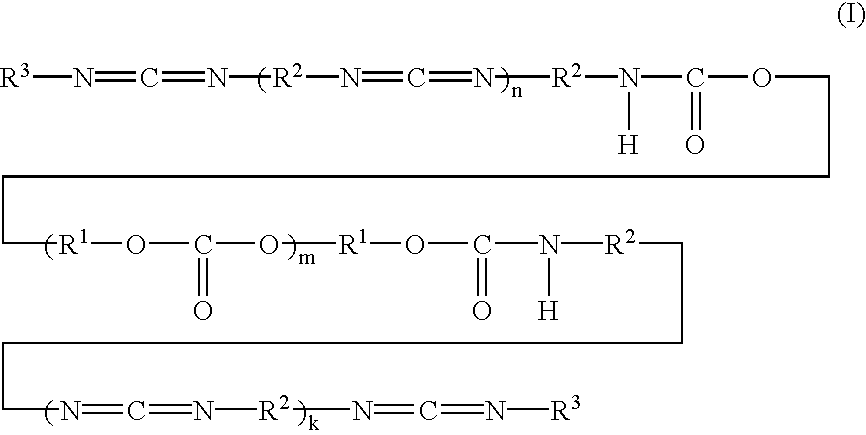
wherein R1 is an alkylene group having 2 to 10 carbon atoms, R2 is a divalent aromatic group, R3 is a monovalent aromatic group, k is 0 or an integer of 1 to 30, m is an integer of 2 to 100, and n is 0 or an integer of 1 to 30, a process for preparing the same and uses of the polycarbodiimide. The polycarbodiimide is favorably used in the form of films such as adhesive films for die bonding and adhesive films for underfilling, which can be used in semiconductor devices.
Description
1. Field of the Invention
The present invention relates to a polycarbodiimide. More specifically, the present invention relates to a polycarbodiimide and its uses, and a process for preparing the polycarbodiimide.
2. Discussion of the Related Art
An aromatic polycarbodiimide has been used in flameproof films and heat-resistant adhesives since the aromatic polycarbodiimide has excellent heat resistance. As the aromatic polycarbodiimide, those prepared by polymerizing monomers such as diphenylmethane diisocyanate (MDI) and tolylene diisocyanate (TDI) have been known.
A film made of the aromatic polycarbodiimide generally has a characteristic such that a volatile gas or a decomposed monomer is not generated from the film even at high temperatures of not less than 400° C.
However, the flexibility of the film is lowered due to self-cross-linking when heat of not less than 200° C. is applied to the film for a long period of time, and the film is not suitable for applications requiring bending because its flexural modulus is so high.
In the process for producing a semiconductor device, a semiconductor chip is bonded to a lead frame or an electrode by coating a paste such as silver paste on a die pad of a lead frame, mounting a semiconductor chip thereon, and curing the paste.
However, since the paste cures even at room temperature, the amount of paste coated changes due to the increase of its viscosity and variation in shape of the paste would be caused during coating, so that variation in reliability of the bonding strength of the semiconductor chip would be caused. For instance, when the amount of the paste coated is changed and insufficient, the bonding strength between the semiconductor chip and the electrode is lowered, so that the semiconductor chip can be peeled off during the subsequent wire bonding step. On the other hand, when the amount of the paste: coated is too large, the paste flows onto the semiconductor chip, so that the yield and the reliability can be lowered. Such defects are even more remarkable for large-sized semiconductor chip, and in order to ensure the reliability of the bonding strength, the amount of coating of the paste should be frequently adjusted, so that there often causes hindrance in workability and productivity.
Recently, in order to achieve the improvement in properties of a semiconductor device, there has been employed a process comprising pouring a liquid thermosetting resin so-called “underfilling material” in a gap between a semiconductor element and a wiring circuit substrate, curing the thermosetting resin to form a resin-cured product, to distribute stress concentrated to an electric connection part into the resin-cured product, thereby improving the reliability of the connection.
However, in order to pour the liquid thermosetting resin between the semiconductor element and the wiring circuit substrate, it is necessary to provide a space for positioning a pouring nozzle near the mounting position of the semiconductor element. With the advancement of miniaturization and thinning of the semiconductor element, it would be difficult to secure the space for positioning a pouring nozzle. Therefore, improvement in the pouring (underfilling) step of the liquid resin has been earnestly desired.
An object of the present invention is to provide a polycarbodiimide which is excellent in flexibility when formed into a film, and maintains low flexural modulus without lowering its flexibility even when the polycarbodiimide is heated at a temperature of not less than 200° C. for a long period of time.
Another object of the present invention is to provide an adhesive film for die bonding which gives a stable bonding strength with no variance in the amount of the film during bonding of a semiconductor chip to an electrode and which is excellent in workability and productivity during processing.
In addition, an object of the present invention is to provide an adhesive film for underfilling which is excellent in relaxation of stress caused in the semiconductor element, the wiring circuit substrate and the connecting electrode, and excellent in reliability of electric connection between the semiconductor element and the wiring circuit substrate, and a semiconductor device in which the adhesive film for underfilling is used as a sealing resin.
These and other objects of the present invention will be apparent from the following description.
According to the present invention, there are provided:
(1) a polycarbodiimide represented by the formula (I): 
wherein R1 is an alkylene group having 2 to 10 carbon atoms, R2 is a divalent aromatic group, R3 is a monovalent aromatic group, k is 0 or an integer of 1 to 30, m is an integer of 2 to 100, and n is 0 or an integer of 1 to 30;
(2) a film made of the above-mentioned polycarbodiimide;
(3) an adhesive film for die bonding, made of the above-mentioned polycarbodiimide;
(4) a semiconductor device comprising a semiconductor chip and an electrode, wherein the semiconductor chip is bonded to the electrode with the aid of the above-mentioned adhesive film for die bonding;
(5) an adhesive film for underfilling, made of the above-mentioned polycarbodiimide;
(6) a semiconductor device comprising a semiconductor element and a wiring circuit substrate, wherein a gap formed between the semiconductor element and the wiring circuit substrate is sealed with the above-mentioned adhesive film for die bonding; and
(7) a process for preparing a polycarbodiimide represented by the formula (I), comprising the steps of:
reacting a polycarbonate diol represented by the formula (II): 
wherein R1 and m are as defined above, with an aromatic diisocyanate in the ratio of not less than 2 mol of the aromatic diisocyanate per one mol of the polycarbonate diol to give a polyurethane having isocyanate groups at both ends; and
carbodiimidating isocyanate groups existing at both ends of the resulting polyurethane with the residual aromatic diisocyanate in the presence of a catalyst.
FIG. 1 is a schematic view showing one embodiment of the semiconductor device of the present invention;
FIG. 2 is a schematic view showing one embodiment of the process for producing the semiconductor device shown in FIG. 1;
FIG. 3 is a schematic view showing another embodiment of the process for producing the semiconductor device shown in FIG. 1;
FIG. 4 is a schematic view showing plural semiconductor elements formed on a semiconductor wafer;
FIG. 5 is a schematic view showing a still another embodiment of the process for producing the semiconductor device shown in FIG. 1;
FIG. 6 is an IR spectrum of a polycarbodiimide obtained in Example 1;
FIG. 7 is an IR spectrum of a polycarbodiimide obtained in Example 2; and
FIG. 8 is an IR spectrum of a polycarbodiimide obtained in Example 3.
The polycarbodiimide of the present invention can be prepared by the steps of reacting a polycarbonate diol represented by the formula (II): 
wherein R1 is an alkylene group having 2 to 10 carbon atoms, and m is an integer of 2 to 100, with an aromatic diisocyanate in the ratio of not less than 2 mol of the aromatic diisocyanate per one mol of the polycarbonate diol to give a polyurethane having isocyanate groups at both ends; and
carbodiimidating isocyanate groups existing at both ends of the resulting polyurethane with the residual aromatic diisocyanate.
In the polycarbonate diol represented by the formula (II), R1 is an alkylene group having 2 to 10 carbon atoms. Examples of the alkylene group include ethylene, tetramethylene, hexamethylene, octamethylene, and the like. The variable m is an integer of 2 to 100, preferably an integer of 5 to 80.
Representative examples of the polycarbonate diol include polyethylenecarbonate diol, polytetramethylenecarbonate diol, polyhexamethylenecarbonate diol, polyoctamethylenecarbonate diol, polydecamethylenecarbonate diol, and the like. These polycarbonate diols can be used alone or in admixture of at least two kinds. Among these polycarbonate diols, polyhexamethylenecarbonate diol is preferable, since it is readily available.
Representative examples of the aromatic diisocyanate include 4,4′-diphenylmethane diisocyanate, 2,6-tolylene diisocyanate, 2,4-tolylene diisocyanate, 1-methoxyphenyl-2,4-diisocyanate, 3,3′-dimethoxy-4,4′-diphenylmethane diisocyanate, 4,4′-diphenyl ether diisocyanate, 3,3′-dimethyl-4,4′-diphenyl ether diisocyanate, 2,2′-bis[4-(4-isocyanatephenoxy)phenyl]hexafluoropropane, 2,2′-bis[4-(4-isocyanatephenoxy)phenyl]propane, 2,2-dimethyl-1,3-bis(4-isocyanatephenoxy)propane, 1,5-bis(4-isocyanatephenoxy)pentane, and the like. These aromatic diisocyanates can be used alone or in admixture of at least two kinds. Among these aromatic diisocyanates, the tolylene diisocyanates are preferable, since they are readily available.
The reaction of the polycarbonate diol represented by the formula (II) with the aromatic diisocyanate can be carried out in an organic solvent.
The organic solvent includes, for instance, halogenated hydrocarbons such as tetrachloroethylene, 1,2-dichloroethane, and chloroform; ketones such as acetone, methyl ethyl ketone, methyl isobutyl ketone and cyclohexanone; cyclic ethers such as tetrahydrofuran and dioxane; aromatic hydrocarbons such as toluene and xylene; and the like. These solvents can be used alone or in admixture of at least two kinds.
It is desired that the amount of the organic solvent is adjusted so that the concentration of the aromatic diisocyanate is usually 5 to 80% by weight, preferably 20 to 70% by weight, from the viewpoints of rapidly progressing the carbodiimidation reaction and facilitating the reaction control.
The amount of the aromatic diisocyanate is not less than 2 mol per one mol of the polycarbonate diol in order that the formed polyurethane can be subsequently carbodiimidated with the residual aromatic diisocyanate, and preferably 4 to 80 mol, more preferably 5 to 50 mol in consideration of flexibility.
The reaction temperature of the polycarbonate diol with the aromatic diisocyanate is usually 0° to 120° C., preferably 20° to 100° C. Although the reaction time cannot be absolutely determined because it differs depending upon the reaction conditions, the reaction time is usually about 1 minute to about 5 hours.
The atmosphere during the reaction can be an atmosphere not containing water. The atmosphere includes, for instance, an inert gas such as nitrogen gas or argon gas, and the like.
The end point of the reaction can be a point at which hydroxyl group of the polycarbonate diol disappears. The disappearance of hydroxyl group can be confirmed by, for instance, NMR or the like.
Thus, the polycarbonate diol is reacted with the aromatic diisocyanate, thereby giving a polyurethane having isocyanate groups at both ends.
Next, the polycarbodiimide represented by the formula (I): 
wherein R1 and m are as defined above, R2 is a divalent aromatic group, R3 is a monovalent aromatic group, k is 0 or an integer of 1 to 30, and n is 0 or an integer of 1 to 30,
is obtained by carbodiimidating isocyanate groups existing at both ends of the resulting polyurethane with the residual aromatic diisocyanate in the presence of a catalyst.
The carbodiimidation can be carried out by using the reaction solution of the polyurethane obtained above without isolating the polyurethane from the reaction solution.
The catalyst used in the carbodiimidation include known phosphorus-containing catalysts. Representative examples of the catalyst include phospholene oxides such as 1-phenyl-2-phospholen-1-oxide, 3-methyl-2-phospholen-1-oxide, 1-ethyl-2-phospholen-1-oxide, 3-methyl-1-phenyl-2-phospholen-1-oxide, and 3-phospholene isomers of these compounds. Among these catalysts, 3-methyl-1-phenyl-2-phospholen-1-oxide is preferable, because it is excellent in reactivity.
It is desired that the amount of the catalyst is 0.01 to 5% by mol, preferably 0.05 to 3% by mol, based on the aromatic diisocyanate, from the viewpoints of shortening the reaction time and avoiding abrupt boiling.
The catalyst can be usually added to the above-mentioned reaction solution.
The carbodiimidation can be carried out by heating a mixed solution prepared by adding a catalyst to the above-mentioned reaction solution to a temperature of usually 40° to 150° C., preferably 50° to 140° C.
The end point of the carbodiimidation can be confirmed by the observation of the absorbance (2140 cm−1) ascribed to carbodiimide group and the disappearance of the absorbance (2280 cm−1) ascribed to isocyanate group, as determined by infrared absorption spectrum (IR).
It is preferable that the end of the formed polycarbodiimide is protected in order to improve the storage stability of the polycarbodiimide solution.
As a protecting agent for protecting the end of the polycarbodiimide, an aromatic monoisocyanate can be used.
Concrete examples of the aromatic monoisocyanate include phenyl isocyanate, p-nitrophenyl isocyanate, m-tolylphenyl isocyanate, p-tolylphenyl isocyanate, p-formylphenyl isocyanate, p-isopropylphenyl isocyanate, and the like. Each of these aromatic monoisocyanates can be used alone, or in admixture of at least two kinds. Among these aromatic monoisocyanates, p-isopropylphenyl isocyanate is preferable, from the viewpoint of storage stability.
The protecting agent may be added at any time of before, beginning, middle or end of the carbodiimidation. Alternatively, the protecting agent may be added over an entire period of the carbodiimidation.
Thus, the reaction solution of the polycarbodiimide represented by the formula (I) is obtained.
By-products contained in the reaction solution can be removed by adsorbing them with an adsorbent.
The adsorbent includes, for instance, alumina gel, silica gel, activated carbon, zeolite, activated magnesium oxide, activated bauxite, fuller's earth, activated clay, molecular sieve carbon, and the like. These adsorbents can be used alone or in admixture of at least two kinds.
When the polycarbodiimide is isolated from the reaction solution, the polycarbodiimide can be precipitated by adding a poor solvent to the reaction solution.
The poor solvent includes, for instance, methanol, ethanol, isopropyl alcohol, hexane, and the like.
The precipitated polycarbodiimide can be collected by filtration or the like, and washed with the above-mentioned poor solvent to remove unreacted monomers and the catalyst. The polycarbodiimide can be dried after washing as occasion demands.
In the polycarbodiimide represented by the formula (I), R1 is an alkylene group having 2 to 10 carbon atoms. Among R1, an alkylene group having 3 to 8 carbon atoms is preferable, and hexamethylene group is more preferable.
R2 is a divalent aromatic group. Concrete examples of R2 include a group represented by the formula (III): 
wherein R4 is an alkyl group having 1 to 4 carbon atoms or an alkoxy group having 1 to 4 carbon atoms,
a group represented by the formula (IV): 
wherein R5 is an alkylene group having 1 to 4 carbon atoms or oxygen atom, and each of R6 and R7 is independently hydrogen atom, an alkyl group having 1 to 4 carbon atoms or an alkoxy group having 1 to 4 carbon atoms,
a group represented by the formula (V): 
wherein X is a group represented by the formula (VI): 
wherein each of R8 and R9 is independently an alkyl group having 1 to 4 carbon atoms which may have a halogen atom, or
a linear or branched alkylene group having 3 to 6 carbon atoms.
In the group represented by the formula (III), R4 is an alkyl group having 1 to 4 carbon atoms or an alkoxy group having 1 to 4 carbon atoms. Among R4, methyl group and methoxy group are preferable.
In the group represented by the formula (IV), R5 is an alkylene group having 1 to 4 carbon atoms or oxygen atom. Among R5, methylene group and oxygen atom are preferable. In addition, each of R6 and R7 is independently hydrogen atom, an alkyl group having 1 to 4 carbon atoms or an alkoxy group having 1 to 4 carbon atoms. Among R6 and R7, hydrogen atom, methyl group and methoxy group are preferable.
In the group represented by the formula (V), X is a group represented by the formula (VI), or a linear or branched alkylene group having 3 to 6 carbon atoms. In the group represented by the formula (VI), each of R8 and R9 is independently an alkyl group having 1 to 4 carbon atoms which may have a halogen atom. The halogen atom includes fluorine atom, chlorine atom, bromine atom and iodine atom. Among them, fluorine atom is preferable. Among the alkyl groups having 1 to 4 carbon atoms which may have a halogen atom, methyl group and trifluoromethyl group are preferable. As the linear or branched alkylene group having 3 to 6 carbon atoms, hexamethylene group and 2,2-dimethylpropylene group are preferable.
Concrete examples of R2 include those represented by the formulae: 
and the like. Among these groups, a group represented by the formula: 
a group represented by the formula: 
are preferable.
When the aromatic diisocyanate is used as a raw material for the polycarbodiimide represented by the formula (I), R2 is an aromatic diisocyanate moiety such as tolylene diisocyanate residue or diphenylmethane diisocyanate residue.
R3 is a monovalent aromatic group. Representative examples of R3 include a group represented by the formula (VII): 
wherein R10 is an alkyl group having 1 to 6 carbon atoms.
R10 is an alkyl group having 1 to 6 carbon atoms, preferably an alkyl group having 1 to 4 carbon atoms, more preferably propyl group. Among R3, the group represented by the formula: 
is preferable. More specifically, R3 is preferably an isopropylphenyl group such as p-isopropylphenyl group.
When the aromatic monoisocyanate is used as a protecting agent during the preparation of the polycarbodiimide represented by the formula (I), R3 is an aromatic monoisocyanate residue such as p-isopropylphenyl isocyanate residue.
The variable k is 0 or an integer of 1 to 30, preferably an integer of 2 to 20. The variable m is an integer of 2 to 100, preferably an integer of 5 to 80. The variable n is 0 or an integer of 1 to 30, preferably an integer of 2 to 20.
It is desired that the average degree of polymerization of the polycarbodiimide represented by the formula (I) [sum of k, m and n in the formula (I)] is 2 to 160, preferably 9 to 120, from the viewpoint of increasing film strength formed by using the polycarbodiimide and the viewpoint of avoiding to readily gelate at ambient temperature in a short period of time.
The polycarbodiimide of the present invention can also be used as a solution prepared by dissolving the polycarbodiimide in an organic solvent. In this case, as the organic solvent, there can be used an organic solvent used for the reaction of the polycarbonate diol with the aromatic diisocyanate. Before the preparation of the polycarbodiimide solution, it is preferable that the polycarbodiimide is previously washed, from the viewpoint of improving stability of the polycarbodiimide solution.
The polycarbodiimide can be suitably used for various applications or uses. The polycarbodiimide can be used as a bonding agent for electronic parts by utilizing its heat resistance. Also, the polycarbodiimide can be suitably used for, for instance, a film, an adhesive film for die bonding, a semiconductor device comprising a semiconductor chip and an electrode, wherein the semiconductor chip is bonded to the electrode with the adhesive film for die bonding; an adhesive film for underfilling; a semiconductor device comprising a semiconductor element and a wiring circuit substrate, wherein a gap between the semiconductor element and the wiring circuit substrate is sealed with the adhesive film for underfilling; and the like.
The process for producing a film made of the polycarbodiimide includes a process for forming a polycarbodiimide solution into a film having an appropriate thickness by a known method such as casting method, spin coating method, roll coating method, or the like; and thereafter heating the formed film to remove a solvent from the solution; and the like.
As the polycarbodiimide solution, there can be used the above-mentioned reaction solution of the polycarbodiimide.
It is desired that the drying temperature is 20° to 350° C., preferably 50° to 250° C., more preferably 70° to 200° C., from the viewpoint of sufficiently removing the solvent from the film and the viewpoint of suppressing thermosetting of the film.
It is desired that the thickness of the film is properly adjusted depending upon its applications or uses. It is desired that the thickness of the film is usually 0.3 μm to 1.5 mm, preferably 0.5 μm to 1 mm, more preferably 1 to 200 μm. In addition, the surface shape and size of the film can be also properly adjusted depending upon the applications or uses of the film, such as lead frames and semiconductor chips.
During the production of the film, there can be added to the polycarbodiimide various additives such as inorganic fillers, lubricants for obtaining surface smoothness, leveling agents, defoaming agents, silane coupling agents for improving adhesiveness, titanium-based coupling agents, and nonionic surfactants, fluorine-containing surfactants, silicone-based adhesive aids as occasion demands within a range so as not to impair workability, heat resistance and the like. The amount of the additive cannot be absolutely determined because the amount differs depending upon its kinds. It is desired that the amount of the additive is usually 0.1 to 100 parts by weight, preferably 0.2 to 50 parts by weight, based on 100 parts by weight of the polycarbodiimide.
The above-mentioned film can be used as an adhesive film. In this case, in order to impart electric conductivity, improve heat conductivity, and control elastic modulus, there can be contained in the film powder of an inorganic material, such as metal such as aluminum, copper, silver, gold, nickel, chromium, lead, tin, zinc or palladium, an alloy such as solder, ceramic such as alumina, silica, magnesia or silicon nitride, or carbon as occasion demands. The amount of the powder cannot be absolutely determined because the amount differs depending upon its kinds. It is desired that the amount of the powder is usually 0.1 to 100 parts by weight preferably 0.2 to 50 parts by weight, based on 100 parts by weight of the polycarbodiimide.
The thickness of the adhesive film cannot be absolutely determined because it differs depending upon its applications or uses. It is desired that the thickness of the adhesive film is usually 0.3 μm to 1.5 mm, preferably 0.5 μm to 1 mm, more preferably 1 to 200 μm.
In addition, the adhesive film can be used by integrating it with a support. The support includes, for instance, metal foils, insulating films, and the like. The metal foil includes thin metal film made of aluminum, copper, silver, gold, nickel, indium, chromium, lead, tin, zinc, palladium, or an alloy thereof. The insulating film includes a film having heat resistance or chemical resistance made of polyamide, polyimide, polyester or the like. Each of the metal foil and the insulating film can be used alone, or they can be used in the form of a laminate comprising at least two layers of the metal foil and the insulating film, for instance, a laminate comprising two layers such as a metal foil/insulating film laminate. Representative examples of the metal foil/ insulating film laminate include, for instance, copper foil/polyimide film laminate, and the like.
The adhesive film can be formed by coating a polycarbodiimide solution on a support to give a laminate of an adhesive film and the support. Alternatively, a previously formed adhesive film can be laminated to a support by means of pressing or the like.
The adhesive film is cured by heating, thereby giving a cured product showing strong adhesive strength and low elastic modulus. Heating can be performed by a means such as a heater or ultrasonication. It is desired that the heating temperature is usually 50° to 300° C., preferably 100 to 250° C. The heating time cannot be absolutely determined depending upon its heating temperature, and is usually 1 second to 30 minutes, preferably 1 second to 3 minutes.
The adhesive film of the present invention has low elastic modulus, and is excellent in flexibility, easily handled, and also excellent in adhesiveness to a semiconductor element and storage stability. Therefore, the adhesive film can be suitably used for adhesion or bonding of various materials, for instance, electric and electronic parts represented by semiconductor chips and lead frames.
In addition, the film of the present invention can be used as an adhesive film for die bonding.
The adhesive film for die bonding can be obtained by forming the film into a strip, and winding the resulting ribbon with a reel or the like. The thickness of the adhesive film for die bonding cannot be absolutely determined because it differs depending upon its applications or uses. It is desired that the thickness of the adhesive film is usually 0.3 μm to 1.5 mm, preferably 0.5 μm to 1 mm, more preferably 1 to 200 μm. In addition, the width of the ribbon can be properly adjusted depending upon its applications or uses.
The adhesive film for die bonding can be used by cutting the adhesive film into given dimensions such as length and shape by an appropriate means such as a cutter.
The adhesive film for die bonding can be suitably used for bonding the semiconductor chip to the electrode in the semiconductor device.
The semiconductor chip can be firmly bonded to the electrode by, for instance, tentatively bonding an adhesive film for die bonding having a desired size to an electrode, for instance, a die pad of a lead frame, mounting a semiconductor chip thereon, and heating the semiconductor chip.
Heating can be performed by a means such as a heater or ultrasonication. It is desired that the heating temperature is usually 50° to 300° C., preferably 100 to 250° C. The heating time cannot be absolutely determined depending upon its heating temperature, and is usually 1 second to 30 minutes, preferably 1 second to 3 minutes.
Thus, since the adhesive film for die bonding is cured by heating, the semiconductor chip is firmly bonded to the electrode.
In addition, according to the present invention, the adhesive film for die bonding is fixed on a dicing apparatus, and one side of a silicone wafer is tentatively bonded to the adhesive film for die bonding at a temperature of room temperature to 90° C. and fixed. Thereafter, the silicon wafer to which the adhesive film is tentatively bonded is cut with the dicing apparatus, so that the semiconductor chip in which the adhesive film for die bonding is retained can be obtained. The adhesive film for die bonding of the resulting semiconductor chip is mounted on an electrode, such as a die pad of a lead frame, and heated, so that the semiconductor chip can be firmly bonded to the electrode. Heating can be carried out by using the same means as mentioned above under the same conditions as mentioned above.
In addition, the film of the present invention can be used as an adhesive film for underfilling. The adhesive film for underfilling can be favorably used for sealing a gap formed between a semiconductor element and a wiring circuit substrate.
The thickness of the adhesive film for underfilling is not limited to specified ones. It is desired that the thickness of the adhesive film for underfilling is 0.3 μm to 1.5 mm, preferably 0.5 μm to 1 mm, more preferably 1 to 200 μm, from the viewpoints of filling the gap between the semiconductor element and the wiring circuit substrate and avoiding hindrance of electric connection between the connecting electrodes.
The size of the adhesive film for underfilling can be properly adjusted in accordance with the size (area) of the semiconductor element mounted. It is preferable that the size of the adhesive film for underfilling is usually about the same size (area) as a semiconductor element.
The gap between the semiconductor element and the wiring circuit substrate can be sealed by, for instance, filling the gap between the semiconductor element and the wiring circuit substrate with an adhesive film for underfilling, and thereafter heating to cure the adhesive film for underfilling. It is desired that the heating temperature is 100° to 225° C., preferably 120° to 200° C. The heating time cannot be absolutely determined depending upon its heating temperature. It is desired that the heating time is usually 3 to 300 minutes, preferably 5 to 180 minutes.
When the gap between the semiconductor element and the wiring circuit substrate is filled with the adhesive film for underfilling, it is preferable that the semiconductor element is usually pressed. The pressure for pressing the semiconductor element can be properly adjusted in accordance with the materials and the number of the connecting electrodes, temperature, and the like. Usually, the pressure per electrode is preferably 0.098 to 4.9 N, more preferably 0.196 to 2.94 N.
Next, a semiconductor device in which a gap formed between a semiconductor element and a wiring circuit substrate is sealed with the adhesive film for underfilling of the present invention will be explained.
FIG. 1 is a schematic explanatory view showing one embodiment of the semiconductor device of the present invention. In FIG. 1, plural connecting electrodes 2 are mounted on one side of a wiring circuit substrate 1. Connecting electrodes 3 corresponding to the connecting electrodes 2 are provided on the surface of a semiconductor element 5. The connecting electrodes 2 are electrically connected with the connecting electrodes 3 by contacting them with each other. A sealing resin layer 4 made of an adhesive film for underfilling is provided between the wiring circuit substrate 1 and the semiconductor element 5. The semiconductor device takes a face-down structure.
The semiconductor device shown in FIG. 1 can be produced by procedures, for instance, shown in FIGS. 2 and 3.
FIG. 2 is a schematic explanatory view showing a laminate comprising a semiconductor element 5 and an adhesive film 6 for underfilling, wherein the semiconductor element 5 is laminated with the adhesive film 6 for underfilling through connecting electrodes 3.
The face of the adhesive film 6 for underfilling of the laminate shown in FIG. 2 is mounted on the connecting electrodes 2 of a wiring circuit substrate 1 as shown in FIG. 3.
Next, the semiconductor element is heated and pressed at a desired temperature and under a desired pressure, so that the adhesive film 6 for underfilling is thermally melted and extruded into the gap between the connecting electrodes 2, 3, and the connecting electrodes 2 are contacted with the connecting electrodes 3, and thereby the connecting electrodes 2 are electrically connected with the connecting electrodes 3, and at the same time the melted adhesive film 6 for underfilling is cured. Thus, as shown in FIG. 1, a sealing resin layer 4 made of an adhesive film for underfilling is formed between the wiring circuit substrate 1 and the semiconductor element 5, so that the wiring circuit substrate 1 and the semiconductor element 5 are electrically connected, and at the same time they are firmly bonded with each other.
The pasting of the adhesive film 6 for underfilling to the semiconductor element 5 can be carried out before or after cutting out the semiconductor element 5 from a semiconductor wafer 7 as shown in FIG. 4.
Another process for producing a semiconductor device comprising a semiconductor element and a wiring circuit substrate, in which a gap formed between the semiconductor element and the wiring circuit substrate is sealed with an adhesive film for underfilling is as follows:
As shown in FIG. 5, using a wiring circuit substrate 1 on which plural connecting electrodes 2 are provided, an adhesive film 6 for underfilling is mounted on the connecting electrodes 2. Next, a semiconductor element provided with connecting electrodes (not illustrated in the figure) is placed on the wiring circuit substrate 1. Thereafter, the semiconductor element is heated and pressed to thermally melt the adhesive film 6 for underfilling and extrude the melted adhesive film 6 into the gap between the connecting electrodes 2 and the connecting electrodes (not illustrated in the figure), and thereby the connecting electrodes 2 are electrically connected with the connecting electrodes (not illustrated in the Figure). At the same time, the melted adhesive film 6 for underfilling is cured to form a sealing resin layer (not illustrated in the figure), and thereby electrical connection and firm bonding between the wiring circuit substrate 1 and the semiconductor element (not illustrated in the figure) are performed.
According to the process, the semiconductor device shown in FIG. 1 can be obtained.
The above-mentioned process for producing the semiconductor device is explained in a case where the semiconductor element is mounted on the wiring circuit substrate. However, the present invention is not limited only to the aforementioned process, and the wiring circuit substrate can be mounted on the semiconductor element.
Next, the present invention will be more specifically described by means of the following examples. All of the preparations were carried out under nitrogen gas stream. Physical properties of the resulting polycarbodiimide were determined in accordance with the following methods.
1. Infrared Absorption (IR) Spectrum
The infrared absorption spectrum was determined by using an IR spectrometer commercially available from JEOL (Nippon Denshi Kabushiki Kaisha) under the product number of FT/IR-230.
2. Initiation Temperature for Thermal Decomposition
The initiation temperature for thermal decomposition was determined by using an analyzer commercially available from Seiko Instruments Inc. under the product number of TG/DTA300. The temperature at which 5% by weight of a polymer was reduced was defined as temperature for 5% by weight reduction (Td).
3. Number-Average Molecular Weight
The number-average molecular weight was determined by using an apparatus commercially available from Tosoh Corporation under the product number of HLC 8120 with a column commercially available from Tosoh Corporation under the product numbers of GMHHR-H+GMHHR-H+G2000HHR and tetrahydrofuran as a developing solvent.
4. Elastic Modulus (E′)
The elastic modulus was determined by using an apparatus for dynamic elastic modulus commercially available from Seiko Instruments Inc. under the product number of DMS210.
5. Glass Transition Temperature (Tg)
The glass transition temperature was determined by using an apparatus for dynamic elastic modulus commercially available from Seiko Instruments Inc. under the product number of DMS210.
6. Adhesive Strength
A 180° peel strength was determined by using an autograph commercially available from Shimadzu Corporation under the product number of AGS-100D.
A 500 mL four-necked flask equipped with a stirrer, a dropping funnel, a reflux condenser and a thermometer was charged with 100 g (0.57 mol) of tolylene diisocyanate commercially available from Takeda Chemical Industries, Ltd. under the trade name of Takenate 80, 100 g (0.10 mol) of a polyhexamethylene carbonatediol commercially available from Ube Industries, Ltd. under the product name of UH-CARB 100, 75 g of xylene and 25 g of cyclohexanone, and the urethanation was carried out at 100° C. for 3 hours.
After the solution was cooled to room temperature, the flask was charged with 0.883 g (4.59 mmol) of a carbodiimidation catalyst (3-methyl-1-phenyl-2-phospholen-1-oxide) and 6.4793 g (40.2 mmol) of p-isopropylphenyl isocyanate, and the mixture was stirred at 100° C. for 2 hours to carry out carbodiimidation, to give a reaction solution of polycarbodiimide. The solvents were removed from the reaction solution, to give a polycarbodiimide.
The IR spectrum of the resulting polycarbodiimide is shown in FIG. 6. As shown in FIG. 6, the carbodiimidation was confirmed on the bases of the observation of the absorption ascribed to carbodiimide group (2140 cm−1) and the disappearance of the absorption ascribed to isocyanate group (2280 cm−1).
The number-average molecular weight of the resulting polycarbodiimide was 6300.
In addition, in the polycarbodiimide represented by the formula (I), m was 7, n was 15 and k was 15, wherein m was calculated on the basis of the identification of end hydroxyl group of the polyhexamethylene carbonate diol, and n and k were calculated on the basis of the number-average molecular weight of the resulting polycarbodiimide. In addition, R1 was hexamethylene group, R2 was composed of 20% by mol of a group represented by the formula: 
and 80% by mol of a group represented by the formula: 
R3 was a group represented by the formula: 
A 500 mL four-necked flask equipped with a stirrer, a dropping funnel, a reflux condenser and a thermometer was charged with 100 g (0.57 mol) of tolylene diisocyanate commercially available from Takeda Chemical Industries, Ltd. under the trade name of Takenate 80, 100 g (0.05 mol) of a polyhexamethylene carbonatediol commercially available from Ube Industries, Ltd. under the product name of UH-CARB 200, 75 g of xylene and 25 g of cyclohexanone, and the urethanation was carried out at 100° C. for 3 hours.
After the solution was cooled to room temperature, the flask was charged with 0.883 g (4.59 mmol) of a carbodiimidation catalyst (3-methyl-1-phenyl-2-phospholen-1-oxide) and 6.4793 g (40.2 mmol) of p-isopropylphenyl isocyanate, and the mixture was stirred at 100° C. for 1 hour to carry out carbodiimidation, to give a reaction solution of polycarbodiimide. The solvents were removed from the reaction solution, to give a polycarbodiimide.
The IR spectrum of the resulting polycarbodiimide is shown in FIG. 7. As shown in FIG. 7, the carbodiimidation was confirmed on the bases of the observation of the absorption ascribed to carbodiimide group (2140 cm−1) and the disappearance of the absorption ascribed to isocyanate group (2280 cm−1).
The number-average molecular weight of the resulting polycarbodiimide was 6000.
In addition, in the polycarbodiimide represented by the formula (I), m was 14, n was 11 and k was 11, wherein m was calculated on the basis of the identification of end hydroxyl group of the polyhexamethylene carbonatediol, and n and k were calculated on the basis of the number-average molecular weight of the resulting polycarbodiimide. In addition, R1 was hexamethylene group, R2 was composed of 20% by mol of a group represented by the formula: 
and 80% by mol of a group represented by the formula: 
R3 was a group represented by the formula: 
A 500 mL four-necked flask equipped with a stirrer, a dropping funnel, a reflux condenser and a thermometer was charged with 100 g (0.57 mol) of tolylene diisocyanate commercially available from Takeda Chemical Industries, Ltd. under the trade name of Takenate 80, 100 g (0.034 mol) of a polyhexamethylene carbonatediol commercially available from Ube Industries, Ltd. under the product name of UH-CARB 300, 112.5 g of xylene and 37.5 g of cyclohexanone, and the urethanation was carried out at 100° C. for 3 hours.
After the solution was cooled to room temperature, the flask was charged with 0.883 g (4.59 mmol) of a carbodiimidation catalyst (3-methyl-1-phenyl-2-phospholen-1-oxide) and 6.4793 g (40.2 mmol) of p-isopropylphenyl isocyanate, and the mixture was stirred at 100° C. for 1 hour to carry out carbodiimidation, to give a reaction solution of polycarbodiimide. The solvents were removed from the reaction solution, to give a polycarbodiimide.
The IR spectrum of the resulting polycarbodiimide is shown in FIG. 8. As shown in FIG. 8, the carbodiimidation was confirmed on the bases of the observation of the absorption ascribed to carbodiimide group (2140 cm−1) and the disappearance of the absorption ascribed to isocyanate group (2280 cm−1).
The number-average molecular weight of the resulting polycarbodiimide was 5400.
In addition, in the polycarbodiimide represented by the formula (I), m was 21, n was 7 and k was 7, wherein m was calculated on the basis of the identification of end hydroxyl group of the polyhexamethylene carbonatediol, and n and k were calculated on the basis of the number-average molecular weight of the resulting polycarbodiimide. In addition, R1 was hexamethylene group, R2 was composed of 20% by mol of a group represented by the formula: 
and 80% by mol of a group represented by the formula: 
R3 was a group represented by the formula: 
The reaction solution of polycarbodiimide obtained in Example 1 was coated on a copper foil having a thickness of 105 μm, and the coating was heated at 90° C. for 30 minutes, and then at 200° C. for 30 minutes, to give an adhesive film having an adhesive layer of 50 μm in thickness, made of the polycarbodiimide.
The thermal properties of the resulting adhesive film were evaluated. As a result, the glass transition temperature (Tg) was 133° C., and the elastic modulus was 940 MPa at 35° C. Also, the temperature for 5% by weight reduction (Td) was 380° C.
The adhesive film was pasted on a 42 alloy plate (the alloy being made of 42% by weight nickel and 58% by weight iron), and the adhesive film was bonded to the 42 alloy plate by pressing under the pressure of 5 MPa at 200° C. for 1 second. The adhesive strength was determined. As a result, the adhesive film exhibited an adhesive strength of 1500 g/cm. The adhesive film was heated at 200° C. with a hot air dryer for one week, and thereafter the adhesive strength was determined. As a result, the adhesive film exhibited an adhesive strength of 1420 g/cm.
In addition, only the adhesive film was heated at 200° C. with a hot air dryer for one week, and thereafter the adhesive film was placed on a flat stand. Whether or not there were any cracks generated in the film was examined after the adhesive film was bended at 180° with a pressure of 1 MPa. The flexibility was evaluated in accordance with the following criteria. The results are shown in Table 1.
[Criteria for Flexibility]
∘: no cracks being generated in the film
X: cracks being generated in the film
Next, the elastic modulus of the film at 35° C. was determined. The elastic modulus was 1100 MPa.
The reaction solution of polycarbodiimide obtained in Example 2 was coated on a copper foil having a thickness of 105 μm, and the coating was heated at 90° C. for 30 minutes, and then at 200° C. for 30 minutes, and dried, to give an adhesive film having an adhesive layer of 50 μm in thickness, made of the polycarbodiimide.
The thermal properties of the resulting adhesive film were evaluated. As a result, the glass transition temperature (Tg) was 129° C., and the elastic modulus was 42 MPa at 35° C. In addition, the temperature for 5% by weight reduction (Td) was 390° C.
The adhesive film was pasted on a 42 alloy plate, and the adhesive film was bonded to the 42 alloy plate by pressing under a pressure of 5 MPa at 200° C. for 1 second. The adhesive strength was determined. As a result, the adhesive film exhibited an adhesive strength of 1550 g/cm. The adhesive film was heated at 200° C. with a hot air dryer for one week, and thereafter the adhesive strength was determined. As a result, the adhesive film exhibited an adhesive strength of 1490 g/cm.
In addition, only the adhesive film was heated at 200° C. with a hot air dryer for one week, and thereafter the flexibility was evaluated in the same manner as in Example 4. The results are shown in Table 1.
Next, the elastic modulus of the film at 35° C. was determined. The elastic modulus was 53 MPa.
The reaction solution of polycarbodiimide obtained in Example 3 was coated on a copper foil having a thickness of 105 μm, and the coating was heated at 90° C. for 30 minutes, and then at 200° C. for 30 minutes, and dried, to give an adhesive film having an adhesive layer of 50 μm in thickness, made of the polycarbodiimide.
The thermal properties of the resulting adhesive film were evaluated. As a result, the glass transition temperature (Tg) was 120° C., and the elastic modulus was 17 MPa at 35° C. In addition, the temperature for 5% by weight reduction (Td) was 395° C.
The adhesive film was pasted on a 42 alloy plate, and the adhesive film was bonded to the 42 alloy plate by pressing under a pressure of 5 MPa at 200° C. for 1 second. The adhesive strength was determined. As a result, the adhesive film exhibited an adhesive strength of 1390 g/cm. The adhesive film was heated at 200° C. with a hot air dryer for one week, and thereafter the adhesive strength was determined. As a result, the adhesive film exhibited an adhesive strength of 1350 g/cm.
In addition, only the adhesive film was heated at 200° C. with a hot air dryer for one week, and thereafter the flexibility was evaluated in the same manner as in Example 4. The results are shown in Table 1.
Next, the elastic modulus of the film at 35° C. was determined. The elastic modulus was 25 MPa.
A 500 mL four-necked flask equipped with a stirrer, a dropping funnel, a reflux condenser and a thermometer was charged with 100 g (0.57 mol) of tolylene diisocyanate commercially available from Takeda Chemical Industries, Ltd. under the trade name of Takenate 80, 75 g of xylene and 25 g of cyclohexanone.
The flask was charged with 0.883 g (4.59 mmol) of a carbodiimidation catalyst (3-methyl-1-phenyl-2-phospholen-1-oxide) and 6.4793 g (40.2 mmol) of p-isopropylphenyl isocyanate, and the mixture was stirred at 100° C. for 1 hour to carry out carbodiimidation, to give a reaction solution of polycarbodiimide. The solvents were removed from the reaction solution, to give a polycarbodiimide.
The IR spectrum of the resulting polycarbodiimide was determined. As a result, the carbodiimidation was confirmed on the bases of the observation of the absorption ascribed to carbodiimide group (2140 cm−1) and the disappearance of the absorption ascribed to isocyanate group (2280 cm−1).
The number-average molecular weight of the resulting polycarbodiimide was 4800.
The resulting reaction solution of polycarbodiimide was coated on a copper foil having a thickness of 105 μm, and the coating was heated at 90° C. for 30 minutes, and then at 200° C. for 30 minutes, and dried, to give an adhesive film having an adhesive layer of 50 μm in thickness, made of the polycarbodiimide.
The thermal properties of the resulting adhesive film were evaluated. As a result, the glass transition temperature (Tg) was 125° C., and the elastic modulus was 3400 MPa at 35° C. In addition, the temperature for 5% by weight reduction (Td) was 400° C.
The adhesive film was pasted on a 42 alloy plate, and the adhesive film was bonded to the 42 alloy plate by pressing under a pressure of 5 MPa at 200° C. for 1 second. The adhesive strength was determined. As a result, the adhesive film exhibited an adhesive strength of 900 g/cm. The adhesive film was heated at 200° C. with a hot air dryer for one week, and thereafter the adhesive strength was determined. As a result, the adhesive film exhibited an adhesive strength of 35 g/cm.
In addition, only the adhesive film was heated at 200° C. with a hot air dryer for one week, and thereafter the flexibility was evaluated in the same manner as in Example 4. The results are shown in Table 1.
Next, the elastic modulus of the film at 35° C. was determined. The elastic modulus was 3400 MPa.
A 500 mL four-necked flask equipped with a stirrer, a dropping funnel, a reflux condenser and a thermometer was charged with 100 g (0.57 mol) of tolylene diisocyanate commercially available from Takeda Chemical Industries, Ltd. under the trade name of Takenate 80, 100 g (0.10 mol) of a polyethylene glycol commercially available from SANYO CHEMICAL INDUSTRIES, LTD. under the product name of PEG-1000, 112.5 g of xylene and 37.5 g of cyclohexanone, and the urethanation was carried out at 100° C. for 3 hours.
After the solution was cooled to room temperature, the flask was charged with 0.883 g (4.59 mmol) of a carbodiimidation catalyst (3-methyl-1-phenyl-2-phospholen-1-oxide) and 6.4793 g (40.2 mmol) of p-isopropylphenyl isocyanate, and the mixture was stirred at 100° C. for 1 hour to carry out carbodiimidation, to give a reaction solution of polycarbodiimide. The solvents were removed from the reaction solution, to give a polycarbodiimide.
The IR spectrum of the resulting polycarbodiimide was determined. As a result, the carbodiimidation was confirmed on the bases of the observation of the absorption ascribed to carbodiimide group (2140 cm−1) and the disappearance of the absorption ascribed to isocyanate group (2280 cm−1).
The number-average molecular weight of the resulting polycarbodiimide was 5800.
Next, the resulting reaction solution of polycarbodiimide was coated on a copper foil having a thickness of 105 μm, and the coating was heated at 90° C. for 30 minutes, and then at 200° C. for 30 minutes, and dried, to give an adhesive film having an adhesive layer of 50 μm in thickness, made of the polycarbodiimide.
The thermal properties of the resulting adhesive film were evaluated. As a result, the glass transition temperature (Tg) was 120° C., and the elastic modulus was 980 MPa at 35° C. In addition, the temperature for 5% by weight reduction (Td) was 230° C.
The adhesive film was pasted on a 42 alloy plate, and the adhesive film was bonded to the 42 alloy plate by pressing under a pressure of 5 MPa at 200° C. for 1 second. The adhesive strength was determined. As a result, the adhesive film exhibited an adhesive strength of 650 g/cm. The adhesive film was heated at 200° C. with a hot air dryer for one week, and thereafter the adhesive strength was determined. As a result, the film exhibited a strength of 0 g/cm.
In addition, only the film was heated at 200° C. with a hot air dryer for one week. As a result, the film did not retain its original shape.
The physical properties of the polycarbodiimides obtained in Examples 1 to 6 and Comparative Examples 1 and 2 are shown in Table 1.
| TABLE 1 | ||||||
| Number- | Physical Properties Just After | Physical Properties of Film After | ||||
| Average | Filming | Heating at 200° C. for one week | ||||
| Molecular | Flexural | Adhesive | Flexural | Adhesive | ||||||
| Weight | Tg | Td | Modulus | Strength | Modulus | Strength | ||||
| (Mn) | (° C.) | (° C.) | (MPa) | (g/cm) | Flexibility | (MPa) | (g/cm) | Flexibility | ||
| Ex. No. | |||||||||
| 4(1) | 6300 | 133 | 380 | 940 | 1500 | ∘ | 1100 | 1420 | |
| 5(2) | 6000 | 129 | 390 | 42 | 1550 | ∘ | 53 | 1490 | |
| 6(3) | 5400 | 120 | 395 | 17 | 1390 | ∘ | 25 | 1350 | |
| Comp. | |||||||||
| Ex. No. | |||||||||
| 1 | 4800 | 125 | 400 | 3400 | 900 | ∘ | 3400 | 35 | x |
| 2 | 5800 | 120 | 230 | 980 | 650 | ∘ | Undeter- | 0 | x |
| minable | |||||||||
It can be seen from the results shown in Table 1 that each of the polycarbodiimides obtained in Examples 4 to 6 (Examples 1 to 3) have low flexural modulus, and are excellent in adhesiveness, flexibility and heat resistance, as compared to the polycarbodiimides obtained in Comparative Examples 1 and 2.
The reaction solution of the polycarbodiimide obtained in Example 1 was coated on a stripping agent-treated separator having a thickness of 50 μm, made of a polyethylene terephthalate film. The coating was heated at 90° C. for 30 minutes, and then at 150° C. for 30 minutes, to give an adhesive film having an adhesive film layer of 50 μm in thickness.
The adhesive strength of the adhesive film for a silicon chip was determined by the following method.
Specifically, the resulting adhesive film was stripped off and removed from the separator, and thereafter cut into squares of 3 cm×3 cm. This film was inserted between silicon chips (passivation: silicon nitride) diced into a size of 2 mm×2 mm×760 μm and a glass-epoxy resin substrate having a size of 3 cm×5 cm, and a load of 2.94 MPa was applied thereto at a temperature of 50° to 200° C. for 40 seconds by using a flip-chip bonder commercially available from Shibuya Kogyo K. K. under the trade name of DB 100. The shearing adhesive strength was determined in accordance with JIS K6852. The results are shown in Table 2.
The same procedures as in Example 7 were carried out except for using the reaction solution of the polycarbodiimide obtained in Example 2 in place of the reaction solution of the polycarbodiimide obtained in Example 1, to give an adhesive film. The shearing adhesive strength of the adhesive film to the silicon chip was determined in the same manner as in Example 7. The results are shown in Table 2.
The same procedures as in Example 7 were carried out except for using the reaction solution of the polycarbodiimide obtained in Example 3 in place of the reaction solution of the polycarbodiimide obtained in Example 1, to give an adhesive film. The shearing adhesive strength of the adhesive film to the silicon chip was determined in the same manner as in Example 7. The results are shown in Table 2.
The same procedures as in Example 7 were carried out except for using the reaction solution of the polycarbodiimide obtained in Comparative Example 1 in place of the reaction solution of the polycarbodiimide obtained in Example 1, to give an adhesive film. The shearing adhesive strength of the adhesive film to the silicon chip was determined in the same manner as in Example 7. The results are shown in Table 2.
The same procedures as in Example 7 were carried out except for using the reaction solution of the polycarbodiimide obtained in Comparative Example 2 in place of the reaction solution of the polycarbodiimide obtained in Example 1, to give an adhesive film. The shearing adhesive strength of the adhesive film to the silicon chip was determined in the same manner as in Example 7. The results are shown in Table 2.
| TABLE 2 | |
| Bond- | |
| ing | Shearing Adhesive Strength (MPa) |
| Temp. | Comparative | Comparative | |||
| (° C.) | Example 7 | Example 8 | Example 9 | Example 3 | Example 4 |
| 50 | 3.5 | 3.7 | 4.0 | 0 | 0.8 |
| 100 | 10.2 | 10.4 | 10.6 | 0 | 2.2 |
| 150 | 24.9 | 22.8 | 24.9 | 8.9 | 10.4 |
| 200 | 35.8 | 34.2 | 37.6 | 12.5 | 13.8 |
| 250 | 40.2 | 39.7 | 40.5 | 18.9 | 19.8 |
It can be seen from the results shown in Table 2 that each of the adhesive films obtained in Examples 7 to 9 exhibits excellent adhesiveness in a wide temperature range of low temperatures to high temperatures, as compared to the adhesive films obtained in Comparative Examples 3 and 4.
The reaction solution of the polycarbodiimide obtained in Example 1 was coated on a stripping agent-treated separator having a thickness of 50 μm, made of a polyethylene terephthalate film. The coating was heated at 150° C. for 30 minutes, to give an adhesive film for underfilling having an adhesive film layer of 100 μm in thickness. The temperature for 5% by weight reduction (Td) was 380° C.
A semiconductor device was produced by using the adhesive film for underfilling. Specifically, as shown in FIG. 2, a wiring circuit substrate 1 (glass-epoxy resin substrate having a thickness of 1 mm) provided with connecting electrodes 3 (material: solder, melting point: 260° C., shape: cylinder having a diameter of 150 μm and a height of 30 μm) were positioned.
Next, the adhesive film was heated and melted under the conditions of a heating temperature of 150° C., a load per one electrode of 0.98 N and a heating time of 1 minute. The melted resin was filled within the gap formed between the wiring circuit substrate 1 and the semiconductor element 5, and the connecting electrodes 2 are contacted with the connecting electrodes 3, to give a tentatively bonded semiconductor device.
Next, the resulting semiconductor device was thermosetted by heating at 150° C. for 60 minutes. As shown in FIG. 1, there were obtained twelve semiconductor devices, the gap of which was filled with the sealing resin 4.
The same procedures as in Example 10 were carried out except for using the reaction solution of the polycarbodiimide obtained in Example 2 in place of the reaction solution of the polycarbodiimide obtained in Example 1, to give an adhesive film for underfilling. The temperature for 5% by weight reduction (Td) was 390° C. A semiconductor device was also produced in the same manner as in Example 10.
The same procedures as in Example 10 were carried out except for using the reaction solution of the polycarbodiimide obtained in Example 3 in place of the reaction solution of the polycarbodiimide obtained in Example 1, to give an adhesive film for underfilling. The temperature for 5% by weight reduction (Td) was 395° C. A semiconductor device was also produced in the same manner as in Example 10.
The same procedures as in Example 10 were carried out except for using the reaction solution of the polycarbodiimide obtained in Comparative Example 1 in place of the reaction solution of the polycarbodiimide obtained in Example 1, to give an adhesive film for underfilling. The temperature for 5% by weight reduction (Td) was 400° C. A semiconductor device was also produced in the same manner as in Example 10.
The same procedures as in Example 10 were carried out except for using the reaction solution of the polycarbodiimide obtained in Comparative Example 2 in place of the reaction solution of the polycarbodiimide obtained in Example 1, to give an adhesive film for underfilling. The temperature for 5% by weight reduction (Td) was 230° C. A semiconductor device was also produced in the same manner as in Example 10.
Electric conductivity of the semiconductor devices obtained in Examples 10 to 12 and Comparative Examples 5 and 6 were examined at 25° C. (initial electric conductivity).
Next, each of the six semiconductor devices obtained in each of Examples and Comparative Examples was subjected to 500 cycles of a thermal shock test (hereinafter referred to as “TST;” test conditions: one cycle comprising a treatment of keeping at −55° C. for 5 minutes and heating at 125° C. for 5 minutes). Thereafter, the electric conductivity of the semiconductor devices was examined (electric conductivity after TST). Also, generation of cracks in the semiconductor element was confirmed. The results are shown in Table 3.
In addition, each of other six semiconductor devices obtained in each of Examples and Comparative Examples was subjected to a pressure cooker test (hereinafter referred to as “PCT;” test conditions: allowing to stand for 168 hours in an atmosphere of a temperature of 121° C. and relative humidity of 100%), without carrying out a TST. Thereafter, the electric conductivity of the other six semiconductor devices obtained in each of Examples and Comparative Examples was examined. The results are also shown in Table 3.
On the other hand, the adhesive film for underfilling obtained in each of Examples and Comparative Examples was heated under the conditions of 150° C. for 60 minutes, to give a cured product. The tensile elastic modulus of each cured product was determined at 35° C. The results are shown in Table 3.
| TABLE 3 | |||
| Comparative | |||
| Examples | Examples | ||
| Test Items | 10 | 11 | 12 | 5 | 6 |
| Tensile Elastic Modulus (MPa) | 940 | 42 | 17 | 3400 | 980 |
| Temperature for 5% by Weight | 380 | 390 | 395 | 400 | 230 |
| Reduction Td (° C.) | |||||
| Initial Electric Conductivity | 0/12 | 0/12 | 0/12 | 0/12 | 0/12 |
| (number of electrodes being | |||||
| not electrically connected per | |||||
| 12 electrodes) | |||||
| Electric Conductivity After TST | 0/6 | 0/6 | 0/6 | 4/6 | 3/6 |
| (number of electrodes being | |||||
| not electrically connected per | |||||
| 6 electrodes) | |||||
| Generation of Cracks in Chips | 0/6 | 0/6 | 0/6 | 4/6 | 2/6 |
| After TST(number of chips | |||||
| cracked per 6 chips) | |||||
| Electric Conductivity After PCT | 0/6 | 0/6 | 0/6 | 2/6 | 4/6 |
| (number of electrodes being | |||||
| not electrically connected per | |||||
| 6 electrodes) | |||||
It can be seen from the results shown in Table 3 that the semiconductor devices obtained in Examples 10 to 12 had no electrically unconnected electrodes or no cracked chips generated in all of the test items.
On the other hand, the semiconductor devices obtained in Comparative Examples 5 and 6 had many faults in the test items.
Therefore, it is ensured that the semiconductor devices obtained in Examples 10 to 12 surely have stable electric conductivity against stress tests such as TST and PCT.
In addition, since the adhesive films obtained in Examples 10 to 12 have low tensile elastic moduli and high temperatures for 5% by weight reduction, and are excellent in heat resistance, the adhesive films can be favorably used as adhesive film for underfilling.
Since the polycarbodiimide of the present invention is excellent in various physical properties such as low elastic modulus, high heat resistance, low hygroscopicity and low dielectric constant, the polycarbodiimide can be favorably used as films, adhesives, and molded products. Especially, the polycarbodiimide of the present invention can be favorably used as adhesive for electronic parts, from the viewpoints of its low elastic modulus and high heat resistance.
As to the adhesive film for die bonding of the present invention, an adhesive layer which is uniform in thickness, shape and the like can readily be formed on electrodes, and fixed at low temperatures such as ambient temperature, so that maintenance of its quality is facilitated. Furthermore, since the adhesive film for die bonding of the present invention can be subjected to firm bonding treatment of the semiconductor chips without necessitating high temperatures and high pressures, the adhesive film has high heat resistance which withstands subsequent steps of wire bonding connection and resin molding sealing.
Since the semiconductor device of the present invention comprises a semiconductor chip and electrodes, wherein the semiconductor chip and the electrodes are firmly bonded with the adhesive film for die bonding, stresses generated in the wire circuit substrate, the semiconductor element and the connecting electrodes can be relaxed. Therefore, the semiconductor device of the present invention exhibits effects of reducing warping of the wire circuit substrate and the semiconductor element, preventing generation of the cracks in the semiconductor element, and improving reliability in electric connection with the connecting electrodes mounted on the wire circuit substrate.
The present invention being thus described, it will be obvious that the same may be varied in many ways. Such variations are not to be regarded as a departure from the spirit and scope of the invention, and all such modifications as would be obvious to one skilled in the art are intended to be included within the scope of the following claims.
Claims (13)
1. A polycarbodiimide represented by the formula (I): 
wherein R1 is an alkylene group having 2 to 10 carbon atoms, R2 is a divalent aromatic group, R3 is a monovalent aromatic group, k is 0 or an integer of 1 to 30, m is an integer of 2 to 100, and n is 0 or an integer of 1 to 30.
2. The polycarbodiimide according to claim 1 , wherein R1 is alkylene group having 3 to 8 carbon atoms.
3. The polycarbodiimide according to claim 2 , wherein R1 is hexamethylene group.
4. The polycarbodiimide according to claim 1 , wherein R2 is a group represented by the formula (III): 
wherein R4 is an alkyl group having 1 to 4 carbon atoms or an alkoxy group having 1 to 4 carbon atoms,
a group represented by the formula (IV): 
wherein R5 is an alkylene group having 1 to 4 carbon atoms or oxygen atom, and each of R6 and R7 is independently hydrogen atom, an alkyl group having 1 to 4 carbon atoms or an alkoxy group having 1 to 4 carbon atoms,
a group represented by the formula (V): 
wherein X is a group represented by the formula (VI): 
wherein each of R8 and R9 is independently an alkyl group having 1 to 4 carbon atoms which may have a halogen atom, or
a linear or branched alkylene group having 3 to 6 carbon atoms.
5. The polycarbodiimide according to claim 4 , wherein R2 is a group represented by the formula: 
a group represented by the formula: 
6. The polycarbodiimide according to claim 1 , wherein R3 is a group represented by the formula (VII): 
wherein R10 is an alkyl group having 1 to 6 carbon atoms.
7. The polycarbodiimide according to claim 6 , wherein R3 is a group represented by the formula: 
8. A film made of the polycarbodiimide of claim 1 .
9. An adhesive film for die bonding, made of the polycarbodiimide of claim 1 .
10. A semiconductor device comprising a semiconductor chip and an electrode, wherein the semiconductor chip is bonded to the electrode with the aid of the adhesive film of claim 9 .
11. An adhesive film for underfilling, made of the polycarbodiimide of claim 1 .
12. A semiconductor device comprising a semiconductor element and a wiring circuit substrate, wherein a gap formed between the semiconductor element and the wiring circuit substrate is sealed with the adhesive film of claim 11 .
13. A process for preparing a polycarbodiimide represented by the formula (I): 
wherein R1 is an alkylene group having 2 to 10 carbon atoms, R2 is a divalent aromatic group, R3 is a monovalent aromatic group, k is 0 or an integer of 1 to 30, m is an integer of 2 to 100, and n is 0 or an integer of 1 to 30,
comprising the steps of:
reacting a polycarbonate diol represented by the formula (II): 
wherein R1 and m are as defined above, with an aromatic diisocyanate in the ratio of not less than 2 mol of the aromatic diisocyanate per one mol of the polycarbonate diol to give a polyurethane having isocyanate groups at both ends; and
carbodiimidating isocyanate groups existing at both ends of the resulting polyurethane with the residual aromatic diisocyanate in the presence of a catalyst.
Applications Claiming Priority (7)
| Application Number | Priority Date | Filing Date | Title |
|---|---|---|---|
| JP2000-264966 | 2000-09-01 | ||
| JP2000264966A JP2002069146A (en) | 2000-09-01 | 2000-09-01 | Polycarbodiimide copolymer and its production method, and sheet-like composition which is made of the same |
| JP2000-299276 | 2000-09-29 | ||
| JP2000299276A JP2002105428A (en) | 2000-09-29 | 2000-09-29 | Adhesive film for die bond and semiconductor device using the same |
| JP2001072074A JP2002265887A (en) | 2001-03-14 | 2001-03-14 | Adhesive film for underfill and semiconductor device using the same |
| JP2001-72074 | 2001-03-14 | ||
| JP2001-072074 | 2001-03-14 |
Publications (2)
| Publication Number | Publication Date |
|---|---|
| US20020055606A1 US20020055606A1 (en) | 2002-05-09 |
| US6492484B2 true US6492484B2 (en) | 2002-12-10 |
Family
ID=27344504
Family Applications (1)
| Application Number | Title | Priority Date | Filing Date |
|---|---|---|---|
| US09/941,559 Expired - Fee Related US6492484B2 (en) | 2000-09-01 | 2001-08-30 | Polycarbodiimide |
Country Status (2)
| Country | Link |
|---|---|
| US (1) | US6492484B2 (en) |
| KR (1) | KR100719828B1 (en) |
Cited By (16)
| Publication number | Priority date | Publication date | Assignee | Title |
|---|---|---|---|---|
| US20030068841A1 (en) * | 2001-09-26 | 2003-04-10 | Nitto Denko Corporation | Process of producing semiconductor device and resin composition sheet used therefor |
| US20040096633A1 (en) * | 2002-11-14 | 2004-05-20 | Nitto Denko Corporation | Adhesive film for underfill and semiconductor device using the same |
| US20040106708A1 (en) * | 2002-11-13 | 2004-06-03 | Yoshihisa Mizumoto | Conductive elastomer composition, conductive member using conductive elastomer composition, image-forming apparatus having conductive member |
| US20040140482A1 (en) * | 2003-01-14 | 2004-07-22 | Nitto Denko Corporation | Semiconductor device and process for producing semiconductor device |
| US20040157992A1 (en) * | 2003-02-04 | 2004-08-12 | Nitto Denko Corporation | Resin for the encapsulation of photosemiconductor element, photosemiconductor device comprising encapsulated optical semiconductor element, and process for producing the device |
| US20040158021A1 (en) * | 2003-02-10 | 2004-08-12 | Nitto Denko Corporation | Polycarbodiimide having high index of refraction and production method thereof |
| US20040176547A1 (en) * | 2003-03-07 | 2004-09-09 | Nitto Denko Corporation | Polycarbodiimide copolymer and production method thereof |
| US20040178423A1 (en) * | 2002-03-26 | 2004-09-16 | Nitto Denko Corporation | Adhesive film for underfill and semiconductor device using the same |
| US20050142379A1 (en) * | 2003-12-26 | 2005-06-30 | Nitto Denko Corporation | Electroluminescence device, planar light source and display using the same |
| US20110021679A1 (en) * | 2008-03-27 | 2011-01-27 | Ikuo Takahashi | Carbodiimide compound, carbodiimide composition and aqueous coating composition |
| US9714378B2 (en) | 2008-10-29 | 2017-07-25 | Basf Se | Proppant |
| US9719011B2 (en) | 2008-10-29 | 2017-08-01 | Basf Se | Proppant |
| WO2020114647A1 (en) | 2018-12-03 | 2020-06-11 | Hfc Prestige International Holding Switzerland S.A.R.L | Multicomponent in situ coloration composition |
| US11478415B2 (en) | 2018-05-03 | 2022-10-25 | Wella International Operations Switzerland Sàrl | Multicomponent composition |
| US11766394B2 (en) | 2018-07-06 | 2023-09-26 | Wella International Operations Switzerland Sarl | Multicomponent composition (Michael addition) |
| US11904042B2 (en) | 2018-07-06 | 2024-02-20 | HFC Prestige International Holding Switzerland S.a.r.l. | Hair coloring composition and methods for its application and removal |
Families Citing this family (4)
| Publication number | Priority date | Publication date | Assignee | Title |
|---|---|---|---|---|
| SG109496A1 (en) * | 2002-04-22 | 2005-03-30 | Saehan Micronics Inc | Composite film and lead frame with composite film attached |
| EP1598383A1 (en) * | 2004-05-21 | 2005-11-23 | Nisshinbo Industries, Inc. | Thermosetting polycarbodiimide copolymer |
| US8778456B2 (en) * | 2011-08-30 | 2014-07-15 | Basf Se | Coating composition including high molecular weight polycarbodiimide, method of preparing same, and method of preparing coating on a substrate |
| BR112014004813A2 (en) | 2011-08-30 | 2017-04-04 | Basf Se | method of producing a high molecular weight polycarbodiimide, high molecular weight polycarbodiimide, and use thereof |
Citations (6)
| Publication number | Priority date | Publication date | Assignee | Title |
|---|---|---|---|---|
| JPH08208788A (en) | 1995-01-31 | 1996-08-13 | Mitsui Toatsu Chem Inc | Polycarbodiimide copolymer and production thereof |
| US6090906A (en) * | 1998-03-20 | 2000-07-18 | Nisshinbo Industries, Inc. | Polycarbodiimide copolymer and process for production thereof |
| US6107448A (en) * | 1997-03-19 | 2000-08-22 | Nitto Denko Corporation | Aromatic polycarbodiimide and films thereof |
| US6121406A (en) * | 1998-04-20 | 2000-09-19 | Nisshinbo Industries, Inc. | Mixture of hydrophilic dicyclohexylmethanecarbodiimide |
| US6180261B1 (en) * | 1997-10-21 | 2001-01-30 | Nitto Denko Corporation | Low thermal expansion circuit board and multilayer wiring circuit board |
| US6248857B1 (en) * | 1998-10-01 | 2001-06-19 | Nitto Denko Corporation | Aromatic polycarbodiimide and polycarbodiimide sheet |
Family Cites Families (5)
| Publication number | Priority date | Publication date | Assignee | Title |
|---|---|---|---|---|
| US5574083A (en) * | 1993-06-11 | 1996-11-12 | Rohm And Haas Company | Aromatic polycarbodiimide crosslinkers |
| JPH0827092A (en) * | 1994-07-15 | 1996-01-30 | Nisshinbo Ind Inc | Urea-modified carbodiimide and production thereof |
| JPH08259693A (en) * | 1995-03-23 | 1996-10-08 | Mitsui Toatsu Chem Inc | Heat-resistant electric wire covering material |
| JPH1060272A (en) * | 1996-08-16 | 1998-03-03 | Nippon Polyurethane Ind Co Ltd | Polycarbodiimide curing agent composition for carboxyl group-containing resin and adhesive and coating material using the same |
| US6063890A (en) * | 1998-07-01 | 2000-05-16 | Basf Corporation | Polycarbodiimide polymers and their use as adhesive intermediate layers in automotive coatings |
-
2001
- 2001-08-30 US US09/941,559 patent/US6492484B2/en not_active Expired - Fee Related
- 2001-08-31 KR KR1020010053294A patent/KR100719828B1/en not_active IP Right Cessation
Patent Citations (6)
| Publication number | Priority date | Publication date | Assignee | Title |
|---|---|---|---|---|
| JPH08208788A (en) | 1995-01-31 | 1996-08-13 | Mitsui Toatsu Chem Inc | Polycarbodiimide copolymer and production thereof |
| US6107448A (en) * | 1997-03-19 | 2000-08-22 | Nitto Denko Corporation | Aromatic polycarbodiimide and films thereof |
| US6180261B1 (en) * | 1997-10-21 | 2001-01-30 | Nitto Denko Corporation | Low thermal expansion circuit board and multilayer wiring circuit board |
| US6090906A (en) * | 1998-03-20 | 2000-07-18 | Nisshinbo Industries, Inc. | Polycarbodiimide copolymer and process for production thereof |
| US6121406A (en) * | 1998-04-20 | 2000-09-19 | Nisshinbo Industries, Inc. | Mixture of hydrophilic dicyclohexylmethanecarbodiimide |
| US6248857B1 (en) * | 1998-10-01 | 2001-06-19 | Nitto Denko Corporation | Aromatic polycarbodiimide and polycarbodiimide sheet |
Cited By (21)
| Publication number | Priority date | Publication date | Assignee | Title |
|---|---|---|---|---|
| US20030068841A1 (en) * | 2001-09-26 | 2003-04-10 | Nitto Denko Corporation | Process of producing semiconductor device and resin composition sheet used therefor |
| US20040178423A1 (en) * | 2002-03-26 | 2004-09-16 | Nitto Denko Corporation | Adhesive film for underfill and semiconductor device using the same |
| US20040106708A1 (en) * | 2002-11-13 | 2004-06-03 | Yoshihisa Mizumoto | Conductive elastomer composition, conductive member using conductive elastomer composition, image-forming apparatus having conductive member |
| US20040096633A1 (en) * | 2002-11-14 | 2004-05-20 | Nitto Denko Corporation | Adhesive film for underfill and semiconductor device using the same |
| US6846550B2 (en) * | 2002-11-14 | 2005-01-25 | Nitto Denko Corporation | Adhesive film for underfill and semiconductor device using the same |
| US20040140482A1 (en) * | 2003-01-14 | 2004-07-22 | Nitto Denko Corporation | Semiconductor device and process for producing semiconductor device |
| US20040157992A1 (en) * | 2003-02-04 | 2004-08-12 | Nitto Denko Corporation | Resin for the encapsulation of photosemiconductor element, photosemiconductor device comprising encapsulated optical semiconductor element, and process for producing the device |
| US20040158021A1 (en) * | 2003-02-10 | 2004-08-12 | Nitto Denko Corporation | Polycarbodiimide having high index of refraction and production method thereof |
| US20040176547A1 (en) * | 2003-03-07 | 2004-09-09 | Nitto Denko Corporation | Polycarbodiimide copolymer and production method thereof |
| US7034101B2 (en) * | 2003-03-07 | 2006-04-25 | Nitto Denko Corporation | Polycarbodiimide copolymer and production method thereof |
| US7018718B2 (en) * | 2003-03-26 | 2006-03-28 | Nitto Denko Corporation | Adhesive film for underfill and semiconductor device using the same |
| US20050142379A1 (en) * | 2003-12-26 | 2005-06-30 | Nitto Denko Corporation | Electroluminescence device, planar light source and display using the same |
| US7722965B2 (en) | 2003-12-26 | 2010-05-25 | Nitto Denko Corporation | Electroluminescence device, planar light source and display using the same |
| US20110021679A1 (en) * | 2008-03-27 | 2011-01-27 | Ikuo Takahashi | Carbodiimide compound, carbodiimide composition and aqueous coating composition |
| US8604154B2 (en) * | 2008-03-27 | 2013-12-10 | Nisshinbo Holdings Inc. | Carbodiimide compound, carbodiimide composition and aqueous coating composition |
| US9714378B2 (en) | 2008-10-29 | 2017-07-25 | Basf Se | Proppant |
| US9719011B2 (en) | 2008-10-29 | 2017-08-01 | Basf Se | Proppant |
| US11478415B2 (en) | 2018-05-03 | 2022-10-25 | Wella International Operations Switzerland Sàrl | Multicomponent composition |
| US11766394B2 (en) | 2018-07-06 | 2023-09-26 | Wella International Operations Switzerland Sarl | Multicomponent composition (Michael addition) |
| US11904042B2 (en) | 2018-07-06 | 2024-02-20 | HFC Prestige International Holding Switzerland S.a.r.l. | Hair coloring composition and methods for its application and removal |
| WO2020114647A1 (en) | 2018-12-03 | 2020-06-11 | Hfc Prestige International Holding Switzerland S.A.R.L | Multicomponent in situ coloration composition |
Also Published As
| Publication number | Publication date |
|---|---|
| US20020055606A1 (en) | 2002-05-09 |
| KR100719828B1 (en) | 2007-05-18 |
| KR20020018602A (en) | 2002-03-08 |
Similar Documents
| Publication | Publication Date | Title |
|---|---|---|
| US6492484B2 (en) | Polycarbodiimide | |
| JP2000053728A (en) | Hardenable underfill encapsulant composition | |
| KR101493595B1 (en) | Polyimide Film | |
| EP1555862A2 (en) | Process for producing circuit board having built-in electronic part | |
| KR20130113377A (en) | Mask sheet for manufacturing semiconductor device and manufacturing method of semiconductor device using the same | |
| JP2992462B2 (en) | Adhesive tape and liquid adhesive for electronic parts | |
| JPH08325533A (en) | Adhesive tape for electronic part and liquid adhesive | |
| KR100621820B1 (en) | Aromatic polycarbodiimide and sheet thereof | |
| KR100310924B1 (en) | Aromatic Polycarbodiimide and Sheets Using the Same | |
| US6228452B1 (en) | Adhesive tape for electronic parts | |
| JP2001072734A (en) | Aromatic polycarbodiimide and water-repellent sheet made therefrom | |
| US20030068841A1 (en) | Process of producing semiconductor device and resin composition sheet used therefor | |
| US6846550B2 (en) | Adhesive film for underfill and semiconductor device using the same | |
| US6045886A (en) | Adhesive tape for electronic parts | |
| JP3650493B2 (en) | Adhesive tape for electronic parts | |
| JP3347651B2 (en) | Adhesive tape for electronic components | |
| JP3839887B2 (en) | Adhesive tape for electronic parts | |
| JP2002105428A (en) | Adhesive film for die bond and semiconductor device using the same | |
| US6001951A (en) | Aromatic polycarbodiimide and film thereof | |
| JP2003174125A (en) | Method of manufacturing semiconductor device and sheet-like resin composition used for the same | |
| JP2002265887A (en) | Adhesive film for underfill and semiconductor device using the same | |
| JP2004292602A (en) | Adhesive film for under fill, and semiconductor device using it | |
| JP2004075788A (en) | Adhesive film for underfill and semiconductor device | |
| JP2000128945A (en) | Aromatic polycarbodiimide and its sheet | |
| JP2003082297A (en) | Adhesive film for die bond and semiconductor device using the same |
Legal Events
| Date | Code | Title | Description |
|---|---|---|---|
| AS | Assignment |
Owner name: NITTO DENKO CORPORATION, JAPAN Free format text: ASSIGNMENT OF ASSIGNORS INTEREST;ASSIGNORS:MISUMI, SADAHITO;HOTTA, YUJI;MATSUMURA, AKIKO;REEL/FRAME:012130/0147 Effective date: 20010803 |
|
| FEPP | Fee payment procedure |
Free format text: PAYOR NUMBER ASSIGNED (ORIGINAL EVENT CODE: ASPN); ENTITY STATUS OF PATENT OWNER: LARGE ENTITY |
|
| FPAY | Fee payment |
Year of fee payment: 4 |
|
| REMI | Maintenance fee reminder mailed | ||
| LAPS | Lapse for failure to pay maintenance fees | ||
| STCH | Information on status: patent discontinuation |
Free format text: PATENT EXPIRED DUE TO NONPAYMENT OF MAINTENANCE FEES UNDER 37 CFR 1.362 |
|
| FP | Lapsed due to failure to pay maintenance fee |
Effective date: 20101210 |