US6441432B1 - High voltage lateral semiconductor device - Google Patents
High voltage lateral semiconductor device Download PDFInfo
- Publication number
- US6441432B1 US6441432B1 US09/442,023 US44202399A US6441432B1 US 6441432 B1 US6441432 B1 US 6441432B1 US 44202399 A US44202399 A US 44202399A US 6441432 B1 US6441432 B1 US 6441432B1
- Authority
- US
- United States
- Prior art keywords
- region
- conductivity
- type
- drain
- well region
- Prior art date
- Legal status (The legal status is an assumption and is not a legal conclusion. Google has not performed a legal analysis and makes no representation as to the accuracy of the status listed.)
- Expired - Lifetime
Links
- 239000004065 semiconductor Substances 0.000 title claims abstract description 51
- 239000000758 substrate Substances 0.000 claims description 53
- 239000002344 surface layer Substances 0.000 claims description 14
- 239000010410 layer Substances 0.000 claims description 7
- 239000012535 impurity Substances 0.000 claims description 4
- 230000002093 peripheral effect Effects 0.000 abstract description 2
- 230000015556 catabolic process Effects 0.000 description 35
- 108091006146 Channels Proteins 0.000 description 10
- 239000000969 carrier Substances 0.000 description 8
- 230000005684 electric field Effects 0.000 description 6
- 238000000034 method Methods 0.000 description 6
- 238000002955 isolation Methods 0.000 description 4
- 238000010586 diagram Methods 0.000 description 2
- 238000002347 injection Methods 0.000 description 2
- 239000007924 injection Substances 0.000 description 2
- 238000004088 simulation Methods 0.000 description 2
- 102000004129 N-Type Calcium Channels Human genes 0.000 description 1
- 108090000699 N-Type Calcium Channels Proteins 0.000 description 1
- XUIMIQQOPSSXEZ-UHFFFAOYSA-N Silicon Chemical compound [Si] XUIMIQQOPSSXEZ-UHFFFAOYSA-N 0.000 description 1
- 230000015572 biosynthetic process Effects 0.000 description 1
- 230000008030 elimination Effects 0.000 description 1
- 238000003379 elimination reaction Methods 0.000 description 1
- 239000012212 insulator Substances 0.000 description 1
- 230000010354 integration Effects 0.000 description 1
- 238000005259 measurement Methods 0.000 description 1
- 230000005855 radiation Effects 0.000 description 1
- 229910052710 silicon Inorganic materials 0.000 description 1
- 239000010703 silicon Substances 0.000 description 1
Images


Classifications
-
- H—ELECTRICITY
- H01—ELECTRIC ELEMENTS
- H01L—SEMICONDUCTOR DEVICES NOT COVERED BY CLASS H10
- H01L29/00—Semiconductor devices adapted for rectifying, amplifying, oscillating or switching, or capacitors or resistors with at least one potential-jump barrier or surface barrier, e.g. PN junction depletion layer or carrier concentration layer; Details of semiconductor bodies or of electrodes thereof ; Multistep manufacturing processes therefor
- H01L29/66—Types of semiconductor device ; Multistep manufacturing processes therefor
- H01L29/68—Types of semiconductor device ; Multistep manufacturing processes therefor controllable by only the electric current supplied, or only the electric potential applied, to an electrode which does not carry the current to be rectified, amplified or switched
- H01L29/76—Unipolar devices, e.g. field effect transistors
- H01L29/772—Field effect transistors
- H01L29/78—Field effect transistors with field effect produced by an insulated gate
- H01L29/7801—DMOS transistors, i.e. MISFETs with a channel accommodating body or base region adjoining a drain drift region
- H01L29/7816—Lateral DMOS transistors, i.e. LDMOS transistors
- H01L29/7824—Lateral DMOS transistors, i.e. LDMOS transistors with a substrate comprising an insulating layer, e.g. SOI-LDMOS transistors
-
- H—ELECTRICITY
- H01—ELECTRIC ELEMENTS
- H01L—SEMICONDUCTOR DEVICES NOT COVERED BY CLASS H10
- H01L29/00—Semiconductor devices adapted for rectifying, amplifying, oscillating or switching, or capacitors or resistors with at least one potential-jump barrier or surface barrier, e.g. PN junction depletion layer or carrier concentration layer; Details of semiconductor bodies or of electrodes thereof ; Multistep manufacturing processes therefor
- H01L29/02—Semiconductor bodies ; Multistep manufacturing processes therefor
- H01L29/06—Semiconductor bodies ; Multistep manufacturing processes therefor characterised by their shape; characterised by the shapes, relative sizes, or dispositions of the semiconductor regions ; characterised by the concentration or distribution of impurities within semiconductor regions
- H01L29/0684—Semiconductor bodies ; Multistep manufacturing processes therefor characterised by their shape; characterised by the shapes, relative sizes, or dispositions of the semiconductor regions ; characterised by the concentration or distribution of impurities within semiconductor regions characterised by the shape, relative sizes or dispositions of the semiconductor regions or junctions between the regions
- H01L29/0692—Surface layout
- H01L29/0696—Surface layout of cellular field-effect devices, e.g. multicellular DMOS transistors or IGBTs
-
- H—ELECTRICITY
- H01—ELECTRIC ELEMENTS
- H01L—SEMICONDUCTOR DEVICES NOT COVERED BY CLASS H10
- H01L29/00—Semiconductor devices adapted for rectifying, amplifying, oscillating or switching, or capacitors or resistors with at least one potential-jump barrier or surface barrier, e.g. PN junction depletion layer or carrier concentration layer; Details of semiconductor bodies or of electrodes thereof ; Multistep manufacturing processes therefor
- H01L29/02—Semiconductor bodies ; Multistep manufacturing processes therefor
- H01L29/06—Semiconductor bodies ; Multistep manufacturing processes therefor characterised by their shape; characterised by the shapes, relative sizes, or dispositions of the semiconductor regions ; characterised by the concentration or distribution of impurities within semiconductor regions
- H01L29/08—Semiconductor bodies ; Multistep manufacturing processes therefor characterised by their shape; characterised by the shapes, relative sizes, or dispositions of the semiconductor regions ; characterised by the concentration or distribution of impurities within semiconductor regions with semiconductor regions connected to an electrode carrying current to be rectified, amplified or switched and such electrode being part of a semiconductor device which comprises three or more electrodes
- H01L29/0843—Source or drain regions of field-effect devices
- H01L29/0847—Source or drain regions of field-effect devices of field-effect transistors with insulated gate
- H01L29/0852—Source or drain regions of field-effect devices of field-effect transistors with insulated gate of DMOS transistors
- H01L29/0856—Source regions
- H01L29/0865—Disposition
-
- H—ELECTRICITY
- H01—ELECTRIC ELEMENTS
- H01L—SEMICONDUCTOR DEVICES NOT COVERED BY CLASS H10
- H01L29/00—Semiconductor devices adapted for rectifying, amplifying, oscillating or switching, or capacitors or resistors with at least one potential-jump barrier or surface barrier, e.g. PN junction depletion layer or carrier concentration layer; Details of semiconductor bodies or of electrodes thereof ; Multistep manufacturing processes therefor
- H01L29/02—Semiconductor bodies ; Multistep manufacturing processes therefor
- H01L29/06—Semiconductor bodies ; Multistep manufacturing processes therefor characterised by their shape; characterised by the shapes, relative sizes, or dispositions of the semiconductor regions ; characterised by the concentration or distribution of impurities within semiconductor regions
- H01L29/08—Semiconductor bodies ; Multistep manufacturing processes therefor characterised by their shape; characterised by the shapes, relative sizes, or dispositions of the semiconductor regions ; characterised by the concentration or distribution of impurities within semiconductor regions with semiconductor regions connected to an electrode carrying current to be rectified, amplified or switched and such electrode being part of a semiconductor device which comprises three or more electrodes
- H01L29/0843—Source or drain regions of field-effect devices
- H01L29/0847—Source or drain regions of field-effect devices of field-effect transistors with insulated gate
- H01L29/0852—Source or drain regions of field-effect devices of field-effect transistors with insulated gate of DMOS transistors
- H01L29/0873—Drain regions
- H01L29/0878—Impurity concentration or distribution
-
- H—ELECTRICITY
- H01—ELECTRIC ELEMENTS
- H01L—SEMICONDUCTOR DEVICES NOT COVERED BY CLASS H10
- H01L29/00—Semiconductor devices adapted for rectifying, amplifying, oscillating or switching, or capacitors or resistors with at least one potential-jump barrier or surface barrier, e.g. PN junction depletion layer or carrier concentration layer; Details of semiconductor bodies or of electrodes thereof ; Multistep manufacturing processes therefor
- H01L29/66—Types of semiconductor device ; Multistep manufacturing processes therefor
- H01L29/68—Types of semiconductor device ; Multistep manufacturing processes therefor controllable by only the electric current supplied, or only the electric potential applied, to an electrode which does not carry the current to be rectified, amplified or switched
- H01L29/76—Unipolar devices, e.g. field effect transistors
- H01L29/772—Field effect transistors
- H01L29/78—Field effect transistors with field effect produced by an insulated gate
- H01L29/7801—DMOS transistors, i.e. MISFETs with a channel accommodating body or base region adjoining a drain drift region
- H01L29/7816—Lateral DMOS transistors, i.e. LDMOS transistors
Definitions
- High voltage MOSFETs are essential devices in the configuration of the output circuit. Even where the MOSFET is not used as an output device, therefore, the output characteristics of high voltage power IC are greatly influenced by the performance of the high voltage MOSFETs, as well as that of the output devices for driving a load.
- n drift region 3 The region interposed between the p well region 4 and n + buffer region 14 (or n + drain region 11 in the absence of the n + buffer region 14 ) is called n drift region 3 , and the width of the n drift region 3 is determined by the required breakdown voltage of the device.
- the cell pattern of FIG. 8 consists of three portions.
- the first region is a portion in which the p well region 4 and n + drain region 11 are disposed in parallel with each other.
- the second region is a portion in which an edge portion (a distal end portion of each tooth of the comb pattern) of the n + drain region 11 is surrounded by the n source region 6 .
- the third region is a portion in which an edge portion (a distal end portion of each tooth of the comb pattern) of the n + source region 6 is surrounded by the n + drain region 11 .
- the second region is called “drain corner” 17
- the third region is called “source corner” 18 .
- the present invention is concerned with the drain corner 17 .
- the first-conductivity-type source region is not formed at the location where the first-conductivity-type drain region would be otherwise surrounded by the source region. With this arrangement, almost no stream of electrons appear in the circular arc portion of the drain corner, thus assuring an increased ON breakdown voltage.
- a high-impurity-concentration second-conductivity-type semiconductor region is formed at the location where the first-conductivity-type source region is not formed.
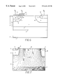
- FIG. 1 is a plan view showing a drain corner of a high voltage lateral semiconductor device according to the first embodiment of the present invention
- FIG. 9 is a plan view showing another surface pattern in which only drain corners are present.
- the lateral MOSFET has an increased ON breakdown voltage.
- the avalanche current started increasing once the drain voltage exceeded 160 V.
- This device with a low capability to withstand avalanche breakdown instantly broke down once the avalanche current started increasing.
- the ON breakdown voltage of the conventional device was 160 V.
- the device of the present invention of FIG. 4 ( a ) did not break down even if the drain voltage exceeded 160 V, or even exceeded 250 V, wile the current slowly increased, thus showing a high capability to withstand breakdown.
- the ON breakdown voltage of the device of the present invention was 270 V.
- the structure of the device of the present invention is considerably effective to increase the ON breakdown voltage.
- the ON breakdown voltage was slightly increased as compared with that of the device of FIG. 1, and the contact resistance was advantageously reduced.
- the ON-state breakdown characteristic can be further improved, and the contact resistance can be advantageously reduced.
Abstract
Description
Claims (4)
Applications Claiming Priority (2)
| Application Number | Priority Date | Filing Date | Title |
|---|---|---|---|
| JP33031598A JP3473460B2 (en) | 1998-11-20 | 1998-11-20 | Horizontal semiconductor device |
| JP10-330315 | 1998-11-20 |
Publications (1)
| Publication Number | Publication Date |
|---|---|
| US6441432B1 true US6441432B1 (en) | 2002-08-27 |
Family
ID=18231270
Family Applications (1)
| Application Number | Title | Priority Date | Filing Date |
|---|---|---|---|
| US09/442,023 Expired - Lifetime US6441432B1 (en) | 1998-11-20 | 1999-11-17 | High voltage lateral semiconductor device |
Country Status (3)
| Country | Link |
|---|---|
| US (1) | US6441432B1 (en) |
| JP (1) | JP3473460B2 (en) |
| NL (1) | NL1013625C2 (en) |
Cited By (17)
| Publication number | Priority date | Publication date | Assignee | Title |
|---|---|---|---|---|
| US20040155258A1 (en) * | 2002-09-12 | 2004-08-12 | Renesas Technology Corp. | Semiconductor device |
| US20060118902A1 (en) * | 2004-12-06 | 2006-06-08 | Matsushita Electric Industrial Co., Ltd. | Lateral semiconductor device and method for producing the same |
| US20060131669A1 (en) * | 2004-12-22 | 2006-06-22 | Douglas Albagli | Thin film transistor for imaging system |
| US20070040212A1 (en) * | 2004-07-15 | 2007-02-22 | Jun Cai | Asymmetric hetero-doped high-voltage mosfet (ah2mos) |
| US20070075393A1 (en) * | 2005-09-30 | 2007-04-05 | Matsushita Electric Industrial Co., Ltd. | Lateral semiconductor device |
| EP1796175A1 (en) * | 2005-12-09 | 2007-06-13 | ATMEL Germany GmbH | DMOS Transistor with optimised peripheral structure |
| US20090133474A1 (en) * | 2003-06-03 | 2009-05-28 | Nano-Proprietary, Inc. | Method and apparatus for sensing hydrogen gas |
| US20090242930A1 (en) * | 2008-03-26 | 2009-10-01 | Fuji Electric Device Technology Co., Ltd. | Semiconductor device |
| US20100013012A1 (en) * | 2004-07-15 | 2010-01-21 | Jun Cai | Integrated complementary low voltage rf-ldmos |
| US20100025756A1 (en) * | 2008-07-30 | 2010-02-04 | Yue Fu | Dual Current Path LDMOSFET with Graded PBL for Ultra High Voltage Smart Power Applications |
| US7692456B2 (en) | 2007-03-30 | 2010-04-06 | Hitachi, Ltd. | Semiconductor integrated circuit capable of directly coupling low-voltage signals with high-voltage signals |
| CN102593181A (en) * | 2012-03-28 | 2012-07-18 | 杭州士兰微电子股份有限公司 | Silicon-on-insulator (SOI) underlay-based high-voltage metal oxide semiconductor tube and manufacturing method |
| CN102637743A (en) * | 2012-05-02 | 2012-08-15 | 杭州士兰微电子股份有限公司 | Power device and manufacturing method thereof |
| US8421153B2 (en) | 2011-03-23 | 2013-04-16 | Kabushiki Kaisha Toshiba | Semiconductor device |
| US20160181361A1 (en) * | 2014-12-17 | 2016-06-23 | Great Wall Semiconductor Corporation | Semiconductor Devices with Cavities |
| CN107316903A (en) * | 2016-04-26 | 2017-11-03 | 中芯国际集成电路制造(上海)有限公司 | UHV LDMOS devices |
| US10211337B2 (en) | 2013-11-12 | 2019-02-19 | Hitachi Automotive Systems, Ltd. | Semiconductor device |
Families Citing this family (6)
| Publication number | Priority date | Publication date | Assignee | Title |
|---|---|---|---|---|
| GB2380056B (en) * | 2001-05-11 | 2005-06-15 | Fuji Electric Co Ltd | Lateral semiconductor device |
| JP4839578B2 (en) * | 2004-04-26 | 2011-12-21 | 富士電機株式会社 | Horizontal semiconductor device |
| JP4972887B2 (en) * | 2005-06-28 | 2012-07-11 | 富士電機株式会社 | Semiconductor device and semiconductor integrated circuit device |
| JP4791113B2 (en) * | 2005-09-12 | 2011-10-12 | オンセミコンダクター・トレーディング・リミテッド | Semiconductor device |
| JP5332112B2 (en) * | 2006-03-29 | 2013-11-06 | 富士電機株式会社 | High voltage lateral MOSFET |
| JP5261927B2 (en) * | 2006-12-11 | 2013-08-14 | パナソニック株式会社 | Semiconductor device |
Citations (1)
| Publication number | Priority date | Publication date | Assignee | Title |
|---|---|---|---|---|
| US5633521A (en) * | 1995-06-01 | 1997-05-27 | Nec Corporation | Enhancement of breakdown voltage in MOSFET semiconductor device |
Family Cites Families (2)
| Publication number | Priority date | Publication date | Assignee | Title |
|---|---|---|---|---|
| JPH1050985A (en) * | 1996-07-31 | 1998-02-20 | Denso Corp | Semiconductor device having mis structure |
| TW400560B (en) * | 1996-12-23 | 2000-08-01 | Koninkl Philips Electronics Nv | Semiconductor device |
-
1998
- 1998-11-20 JP JP33031598A patent/JP3473460B2/en not_active Expired - Lifetime
-
1999
- 1999-11-17 US US09/442,023 patent/US6441432B1/en not_active Expired - Lifetime
- 1999-11-19 NL NL1013625A patent/NL1013625C2/en not_active IP Right Cessation
Patent Citations (1)
| Publication number | Priority date | Publication date | Assignee | Title |
|---|---|---|---|---|
| US5633521A (en) * | 1995-06-01 | 1997-05-27 | Nec Corporation | Enhancement of breakdown voltage in MOSFET semiconductor device |
Cited By (39)
| Publication number | Priority date | Publication date | Assignee | Title |
|---|---|---|---|---|
| US20040155258A1 (en) * | 2002-09-12 | 2004-08-12 | Renesas Technology Corp. | Semiconductor device |
| US6847058B2 (en) * | 2002-09-12 | 2005-01-25 | Renesas Technology Corp. | Semiconductor device |
| US20050151186A1 (en) * | 2002-09-12 | 2005-07-14 | Renesas Technology Corp. | Semiconductor device |
| US20080149972A1 (en) * | 2002-09-12 | 2008-06-26 | Katuo Ishizaka | Semiconductor device |
| US7312501B2 (en) | 2002-09-12 | 2007-12-25 | Renesas Technology Corp. | Semiconductor device |
| US20090133474A1 (en) * | 2003-06-03 | 2009-05-28 | Nano-Proprietary, Inc. | Method and apparatus for sensing hydrogen gas |
| US8324042B2 (en) | 2004-07-15 | 2012-12-04 | Fairchild Semiconductor Corporation | Integrated complementary low voltage RF-LDMOS |
| US20100084686A1 (en) * | 2004-07-15 | 2010-04-08 | Jun Cai | Assymetric hetero-doped high-voltage mosfet (ah2mos) |
| US20100013012A1 (en) * | 2004-07-15 | 2010-01-21 | Jun Cai | Integrated complementary low voltage rf-ldmos |
| US7888735B2 (en) * | 2004-07-15 | 2011-02-15 | Fairchild Semiconductor Corporation | Integrated complementary low voltage RF-LDMOS |
| US20070040212A1 (en) * | 2004-07-15 | 2007-02-22 | Jun Cai | Asymmetric hetero-doped high-voltage mosfet (ah2mos) |
| US7649225B2 (en) * | 2004-07-15 | 2010-01-19 | Fairchild Semiconductor Corporation | Asymmetric hetero-doped high-voltage MOSFET (AH2MOS) |
| US20110104861A1 (en) * | 2004-07-15 | 2011-05-05 | Jun Cai | Integrated complementary low voltage rf-ldmos |
| US7238987B2 (en) | 2004-12-06 | 2007-07-03 | Matsushita Electric Industrial Co., Ltd. | Lateral semiconductor device and method for producing the same |
| US20060118902A1 (en) * | 2004-12-06 | 2006-06-08 | Matsushita Electric Industrial Co., Ltd. | Lateral semiconductor device and method for producing the same |
| US20060131669A1 (en) * | 2004-12-22 | 2006-06-22 | Douglas Albagli | Thin film transistor for imaging system |
| US20070075393A1 (en) * | 2005-09-30 | 2007-04-05 | Matsushita Electric Industrial Co., Ltd. | Lateral semiconductor device |
| US7323747B2 (en) * | 2005-09-30 | 2008-01-29 | Matsushita Electric Industrial, Co., Ltd. | Lateral semiconductor device |
| CN100466289C (en) * | 2005-12-09 | 2009-03-04 | Atmel德国有限公司 | DMOS transistor with optimized periphery structure |
| US20070132019A1 (en) * | 2005-12-09 | 2007-06-14 | Atmel Germany Gmbh | DMOS transistor with optimized periphery structure |
| US7521756B2 (en) | 2005-12-09 | 2009-04-21 | Atmel Germany Gmbh | DMOS transistor with optimized periphery structure |
| EP1796175A1 (en) * | 2005-12-09 | 2007-06-13 | ATMEL Germany GmbH | DMOS Transistor with optimised peripheral structure |
| US7973573B2 (en) | 2007-03-30 | 2011-07-05 | Hitachi, Ltd. | Semiconductor integrated circuit device |
| US20100137720A1 (en) * | 2007-03-30 | 2010-06-03 | Hitachi, Ltd. | Semiconductor integrated circuit device |
| US7692456B2 (en) | 2007-03-30 | 2010-04-06 | Hitachi, Ltd. | Semiconductor integrated circuit capable of directly coupling low-voltage signals with high-voltage signals |
| US8502344B2 (en) | 2008-03-26 | 2013-08-06 | Fuji Electric Co., Ltd. | Semiconductor device |
| US20090242930A1 (en) * | 2008-03-26 | 2009-10-01 | Fuji Electric Device Technology Co., Ltd. | Semiconductor device |
| US20100025756A1 (en) * | 2008-07-30 | 2010-02-04 | Yue Fu | Dual Current Path LDMOSFET with Graded PBL for Ultra High Voltage Smart Power Applications |
| US7851857B2 (en) * | 2008-07-30 | 2010-12-14 | Freescale Semiconductor, Inc. | Dual current path LDMOSFET with graded PBL for ultra high voltage smart power applications |
| US20130270637A1 (en) * | 2011-03-23 | 2013-10-17 | Kabushiki Kaisha Toshiba | Semiconductor device |
| US8421153B2 (en) | 2011-03-23 | 2013-04-16 | Kabushiki Kaisha Toshiba | Semiconductor device |
| CN102593181A (en) * | 2012-03-28 | 2012-07-18 | 杭州士兰微电子股份有限公司 | Silicon-on-insulator (SOI) underlay-based high-voltage metal oxide semiconductor tube and manufacturing method |
| CN102637743A (en) * | 2012-05-02 | 2012-08-15 | 杭州士兰微电子股份有限公司 | Power device and manufacturing method thereof |
| CN102637743B (en) * | 2012-05-02 | 2015-04-29 | 杭州士兰微电子股份有限公司 | Power device and manufacturing method thereof |
| US10211337B2 (en) | 2013-11-12 | 2019-02-19 | Hitachi Automotive Systems, Ltd. | Semiconductor device |
| US20160181361A1 (en) * | 2014-12-17 | 2016-06-23 | Great Wall Semiconductor Corporation | Semiconductor Devices with Cavities |
| US9666703B2 (en) * | 2014-12-17 | 2017-05-30 | Great Wall Semiconductor Corporation | Semiconductor devices with cavities |
| US10153167B2 (en) | 2014-12-17 | 2018-12-11 | Great Wall Semiconductor Corporation | Semiconductor devices with cavities |
| CN107316903A (en) * | 2016-04-26 | 2017-11-03 | 中芯国际集成电路制造(上海)有限公司 | UHV LDMOS devices |
Also Published As
| Publication number | Publication date |
|---|---|
| NL1013625C2 (en) | 2004-09-16 |
| NL1013625A1 (en) | 2000-05-23 |
| JP3473460B2 (en) | 2003-12-02 |
| JP2000156495A (en) | 2000-06-06 |
Similar Documents
| Publication | Publication Date | Title |
|---|---|---|
| US6441432B1 (en) | High voltage lateral semiconductor device | |
| US20020053717A1 (en) | Semiconductor apparatus | |
| JP2973588B2 (en) | MOS type semiconductor device | |
| US7948058B2 (en) | Semiconductor device and semiconductor integrated circuit device for driving plasma display using the semiconductor device | |
| JPH0396282A (en) | Insulated-gate semiconductor device | |
| JPH07245394A (en) | Insulation gate bipolar transistor | |
| US5889310A (en) | Semiconductor device with high breakdown voltage island region | |
| JP3076468B2 (en) | Semiconductor device | |
| US7741695B2 (en) | Semiconductor device | |
| JPH07169868A (en) | Circuit pattern having at least one bipolar power device | |
| US5608238A (en) | Semiconductor device having two insulated gates and capable of thyristor function and method for operating the same | |
| JPH03194974A (en) | Mos type semiconductor device | |
| US7655977B2 (en) | Trench IGBT for highly capacitive loads | |
| US5874767A (en) | Semiconductor device including a lateral power device | |
| US20130248926A1 (en) | Semiconductor device | |
| US5440164A (en) | MOS/bipolar device | |
| US20020027253A1 (en) | Circuit incorporated IGBT and power conversion device using the same | |
| JP3226075B2 (en) | Vertical MOS semiconductor device | |
| JPH1065018A (en) | Semiconductor device | |
| JP3249891B2 (en) | Semiconductor device and method of using the same | |
| US4969024A (en) | Metal-oxide-semiconductor device | |
| US5349232A (en) | Protection diode for a vertical semiconductor component | |
| US20090315072A1 (en) | Semiconductor Device, Semiconductor Integrated Circuit Equipment Using the Same for Driving Plasma Display, and Plasma Display Unit | |
| KR100510436B1 (en) | Horizontal Insulated Gate Bipolar Transistor | |
| JP3196575B2 (en) | Composite semiconductor device and power conversion device using the same |
Legal Events
| Date | Code | Title | Description |
|---|---|---|---|
| AS | Assignment |
Owner name: FUJI ELECTRIC CO., LTD., JAPAN Free format text: ASSIGNMENT OF ASSIGNORS INTEREST;ASSIGNOR:SUMIDA, HITOSHI;REEL/FRAME:010410/0488 Effective date: 19991001 |
|
| STCF | Information on status: patent grant |
Free format text: PATENTED CASE |
|
| FPAY | Fee payment |
Year of fee payment: 4 |
|
| FPAY | Fee payment |
Year of fee payment: 8 |
|
| AS | Assignment |
Owner name: FUJI ELECTRIC SYSTEMS CO., LTD.,JAPAN Free format text: ASSIGNMENT OF ASSIGNORS INTEREST;ASSIGNOR:FUJI ELECTRIC DEVICE TECHNOLOGY CO., LTD.;REEL/FRAME:024252/0451 Effective date: 20090930 Owner name: FUJI ELECTRIC SYSTEMS CO., LTD., JAPAN Free format text: ASSIGNMENT OF ASSIGNORS INTEREST;ASSIGNOR:FUJI ELECTRIC DEVICE TECHNOLOGY CO., LTD.;REEL/FRAME:024252/0451 Effective date: 20090930 |
|
| AS | Assignment |
Owner name: FUJI ELECTRIC CO., LTD., JAPAN Free format text: MERGER AND CHANGE OF NAME;ASSIGNORS:FUJI ELECTRIC SYSTEMS CO., LTD. (FES);FUJI TECHNOSURVEY CO., LTD. (MERGER BY ABSORPTION);REEL/FRAME:026970/0872 Effective date: 20110401 |
|
| FPAY | Fee payment |
Year of fee payment: 12 |