US6377633B1 - Apparatus and method for decoding asynchronous data - Google Patents
Apparatus and method for decoding asynchronous data Download PDFInfo
- Publication number
- US6377633B1 US6377633B1 US09/169,517 US16951798A US6377633B1 US 6377633 B1 US6377633 B1 US 6377633B1 US 16951798 A US16951798 A US 16951798A US 6377633 B1 US6377633 B1 US 6377633B1
- Authority
- US
- United States
- Prior art keywords
- negative
- peak
- signal
- signal value
- value
- Prior art date
- Legal status (The legal status is an assumption and is not a legal conclusion. Google has not performed a legal analysis and makes no representation as to the accuracy of the status listed.)
- Expired - Lifetime
Links
Images


Classifications
-
- H—ELECTRICITY
- H03—ELECTRONIC CIRCUITRY
- H03K—PULSE TECHNIQUE
- H03K5/00—Manipulating of pulses not covered by one of the other main groups of this subclass
- H03K5/01—Shaping pulses
- H03K5/08—Shaping pulses by limiting; by thresholding; by slicing, i.e. combined limiting and thresholding
- H03K5/082—Shaping pulses by limiting; by thresholding; by slicing, i.e. combined limiting and thresholding with an adaptive threshold
- H03K5/086—Shaping pulses by limiting; by thresholding; by slicing, i.e. combined limiting and thresholding with an adaptive threshold generated by feedback
-
- H—ELECTRICITY
- H04—ELECTRIC COMMUNICATION TECHNIQUE
- H04L—TRANSMISSION OF DIGITAL INFORMATION, e.g. TELEGRAPHIC COMMUNICATION
- H04L25/00—Baseband systems
- H04L25/02—Details ; arrangements for supplying electrical power along data transmission lines
- H04L25/06—Dc level restoring means; Bias distortion correction ; Decision circuits providing symbol by symbol detection
- H04L25/061—Dc level restoring means; Bias distortion correction ; Decision circuits providing symbol by symbol detection providing hard decisions only; arrangements for tracking or suppressing unwanted low frequency components, e.g. removal of dc offset
- H04L25/062—Setting decision thresholds using feedforward techniques only
Definitions
- This invention relates to the field of asynchronous data communications, and more particularly, this invention relates to the field of decoding asynchronous digital data that is sent over a wire line, radio, or fiber optic communication channel.
- Asynchronous communication systems are commonly used where data is not time oriented and is sent in bursts and received often in a burst receiver.
- knowledge of the data amplitude should be ascertained in order to establish a reference within a communications receiver.
- Any receiver also should typically be capable of performing DC signal restoration during potentially long “quiet” periods.
- An example of a “quiet” period is shown in FIG. 1, where a frame of data has a stop bit, intermediate data (represented by the letter D) and a stop bit, followed by a two minute signal delay, followed by another frame of data with a start and stop bit and intermediate data (D).
- Asynchronous digital data is often sent over a wire line, radio link, or fiber optic communication channel.
- analog implementations have been used for decoding the asynchronous signals.
- decoding circuits have been designed to take into consideration the length of a communication line or the link loss. In this type of system, the circuit will restore an analog signal to obtain a digital signal value and then make a decoding decision on the digital signal value.
- the circuit is designed based on knowledge of the difference in data amplitude coming into a communications receiver, such as in a fiber optic communications system.
- the receiver could move even if the transmission distance and theoretical amount of attenuation is known.
- the link loss would not be known and the signal strength could be variable.
- the communication line could be from room-to-room, or from city-to-city.
- the circuit is designed based on the theoretical amount of signal attenuation.
- asynchronous data communication is the transmittal of packets or frames.
- a burst receiver may be used as mentioned before.
- the receiver will lose its DC reference over a time pause in signal communication, which is why many communication systems use Manchester encoding or pseudo random number generation.
- An example of one problem with DC signal restoration is comparing the difference between transmitting asynchronous data over three feet of cable between two computers in the same room, as compared to a longer distance system.
- asynchronous data communication system if logical 1 corresponds to five volts and logical 0 corresponds to zero volts, there would be little problem in finding the midpoint reference or threshold when the data signal is transmitted through only three to five feet of cable. However, it the data signal is transmitted through 100 miles of cable, then the final attenuation would be great and the final signal could be about 100 millivolts.
- Some analog devices that are used for measuring the signal attenuation and setting a signal threshold in a receiver have been implemented with asynchronous data communications, but these systems do not accomplish high dynamic range burst mode asynchronous data decisions because of thermal drifts and parasitic effects of passive and active components.
- a preamble system In a preamble system, several disposable data bits are sent prior to a data payload having the start bit to allow a decision circuit in the communications receiver to establish a signal reference, Thus, as soon as a start bit is transmitted, the circuitry has measured both zero and one logic levels and has set a threshold half-way between the zero and one logic levels.
- a continuous stream of data is sent with an even mix of ones and zeros by using a randomizing circuit.
- the data is multiplied by a pseudo random number in the transmitter to ensure the data stream is rich in data transitions. Thus, there will always be ones and zeros that are transmitted. Then the communications receiver circuitry decodes the pseudo random number and extracts the information.
- AGC automatic gain control
- a constant automatic gain control circuit controls the communications receiver gain. For example, if the transmission line is 100 miles long and there is a 100 millivolt threshold, then the signal will be amplified back to five volts. As a result, the system would use a 2.5 volt reference. However, there are time constants. If the system is quiet for extended periods, for example, about two minutes or some other time period, then the signal will decay and there is no signal information on which to make a gain or adjustment of the signal. Thus, the DC signal information is not present.
- the preamble system reduces the data rate of the channel.
- the preamble method prevents binary data transfer. Certain characters could be sent as a preamble and would, therefore, not be used for the information content. For example, if bits are sent to a communications receiver in order to synchronize that receiver, then no data information is sent.
- the preamble system requires a preamble and prevents binary data transfer. If binary data is transmitted, there could be no start bit. The preamble system would not know the difference between a binary data bit or preamble bit. There could also never be a “sync” word in the binary transmission because it would mistake it for a frame signal.
- AGC automatic gain control system
- U.S. Pat. No. 5,052,021 to Goto et al. U.S. Pat. No. 4,823,360 to Tremblay et al.
- the present invention is advantageous because it now provides long term circuit stability and accomplishes high dynamic range burst mode asynchronous data decision decoding of asynchronous data communication signals with relatively long periods of absent data without losing a reference. It is possible to use the decoding apparatus and method of the present invention in any product that sends asynchronous digital data over a wire line, radio, or fiber optic communication channel where the distance and loss characteristics of the channel are unknown or widely variable.
- asynchronous data signals are digitally decoded by measuring the amplitude of a signal bit having negative and positive peak values, and digitally computing a mid-bit reference from the signal bit. Changes in the base band signal peak excursions are tracked and the mid-bit reference is updated from the tracked changes of the base band signal excursions.
- the positive and negative peak registers are periodically decremented and incremented, respectfully, at a rate several orders of magnitude slower than the ADC sample rate.
- the apparatus digitally decodes asynchronous communication signals and includes an analog-to-digital converter for converting analog communication signals having negative and positive signal peaks into binary signal values corresponding to the analog communication signals.
- a negative peak register and a positive peak register store negative and positive peak signal values and the minimum negative and maximum positive signal values corresponding to the minimum, most negative peak signal value and the maximum, most positive signal value.
- a negative peak comparator and a positive peak comparator compare the positive and negative signal peaks of a currently received binary signal value with the minimum negative and maximum positive peak signal value stored within the negative and positive peak registers so as to update the negative and positive peak registers with any new minimum negative and maximum positive peak signal values.
- a subtraction circuit subtracts the positive peak signal value from the negative peak signal value to determine the magnitude signal value corresponding to the difference between a binary zero and one of the binary signal values.
- An addition circuit adds one-half of the magnitude signal value to the minimum negative peak signal value stored in the negative peak register to obtain a threshold signal value used to determine the mid-bit reference.
- the analog-to-digital converter converts an analog communication signal into an N-bit value.
- the N-bit value can comprise a 12-bit value.
- a threshold register also stores the threshold signal value.
- a threshold comparator compares the threshold signal value to a currently received binary signal value corresponding to a currently received and converted analog communication signal.
- a circuit latch can also be included for latching a single bit from an N-bit value.
- An analog-to-digital buffer register can store the binary signal values that have been converted from the analog communication signals.
- the method of the present invention digitally decodes asynchronous communication signals, and comprises the steps of converting analog communication signals having negative and positive peak values into binary digital signal values.
- the method also comprises the step of storing in respective negative and positive peak registers at least the negative and positive peak signal values.
- the method further comprises the step of comparing the negative and positive peak signal values of a currently received binary signal value with the minimum negative and maximum positive peak signal values stored within the negative and positive peak registers, and updating the negative and positive peak registers with the new minimum negative and maximum positive peak signal values when the comparison step determines that there is a new minimum negative or maximum positive peak signal value.
- the magnitude signal value corresponding to the peak-to-peak signal excursion is also determined in a subtraction circuit by determining the difference between a digital one and digital zero.
- the minimum negative peak signal value stored in the negative peak register is added to one-half of the magnitude signal value, resulting in a threshold signal value.
- the method further comprises the step of initially measuring the amplitude of the signal start bit.
- the peak-to-peak excursion is calculated and half of that calculated peak-to-peak excursion value is added to the minimum measured value corresponding to the minimum negative peak signal value to obtain a mid-bit reference.
- the method includes the step of tracking changes of base band signal peak excursions by measuring the currently received or “sampled” negative and positive peak signal values and comparing those negative and positive peak signal values with previously determined minimum negative and maximum positive peak signal values that are stored within respective negative and positive peak registers.
- the analog communication signals are converted into a binary signal values with the analog-to-digital converter and stored in an analog-to-digital buffer register.
- the analog communication sample can be oversampled by about ten times.
- the method also comprises the step of converting the analog communication signal into an N-bit value that typically is a 12-bit value.
- the method also includes the steps of decrementing the positive peak register and incrementing the negative peak register periodically, which in one aspect of the present invention, is about one Hz rate.
- the method also includes the steps of determining the magnitude signal value corresponding to the difference between a binary zero and one and the binary digital signal by subtracting the positive peak signal value from the negative peak signal value and dividing the magnitude value by two within the division circuit and then adding the result of the division step to a minimum negative peak signal value that is stored within the negative peak register.
- FIG. 1 is a representation of an asynchronous communication data transmission that shows a first frame transmission having a start and stop bit and data located between the start and stop bit followed by a two minute delay, and followed, in turn, by a second frame transmission.
- FIG. 2 is a graph showing the dynamic range limitations of a typical digital sampler that is capable of DC restoration with an optimal decision circuit reference level and a default decision circuit reference level where the receiver noise floor is shown by the bottom line.
- FIG. 3 is a graph similar to the graph of FIG. 2, but showing a signal with a small extinction ratio.
- FIG. 4 is a block diagram of the apparatus for digitally decoding asynchronous signals in accordance with the present invention.
- FIG. 5 is a flow chart illustrating the basic method for digitally decoding asynchronous data signals of the present invention.
- the present invention is advantageous because it now allows a high dynamic range for decoding asynchronous digital data and the increased stability of digital computational circuits.
- the apparatus and method of the present invention can be used with any product that sends asynchronous digital data over a wire line, radio, or fiber optic communication channel, where the distance and loss characteristics of the channel are unknown or widely variable.
- the amplitude of a signal bit having negative and positive peak values is determined, followed by digitally computing a mid-bit reference based on the mid-bit determination. Changes of base band signal peak excursions are tracked and the mid-bit reference is updated from the tracked changes of the base band signal peak excursions.
- the apparatus includes a negative peak register and positive peak register for storing the negative and positive peak signal values and the minimum negative and maximum positive peak signal values corresponding to the minimum, most negative peak signal value and the maximum, most positive signal value.
- a negative peak comparator and positive peak comparator compares the positive and negative peak signal values of a currently received binary bit signal with the minimum negative and maximum positive peak signal values stored within the negative and positive peak registers, and updates the negative and positive peak registers with any new minimum negative and maximum positive peak signal values.
- An addition circuit adds one-half of the magnitude signal value of a binary signal to the minimum negative peak signal value stored in the negative peak register to obtain a threshold signal value that is then used to update the mid-bit reference.
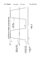
- FIG. 1 illustrates a graphical representation of an asynchronous data frame transmission shown at 10 , with a delay that causes a time delay problem that the apparatus and method of the present invention solves adequately.
- asynchronous data communication signals send data in bursts and are not time oriented.
- a first frame 12 could include a start bit 14 and stop bit 16 , with data bits (D) located between the start and stop bit 14 , 16 .
- the transmission then may have a two minute delay 18 followed by a second frame 20 having a start bit 22 and stop bit 22 and data (D) located between start and stop bits 22 , 24 .
- the communications receiver In order to decode the incoming data correctly, knowledge of the data amplitude must be known in order to establish a reference in a communications receiver.
- the communications receiver should also be capable of performing DC restoration during potentially long quiet periods, such as the illustrated two minute delay 18 .
- the present invention solves this problem as compared to those prior art systems that use (a) a preamble to reduce the data rate of a channel, (b) a continuous transmission, or (c) an automatic gain control to solve amplitude fluctuations, but not DC restoration.
- FIG. 2 illustrates a graphical representation of the dynamic range limitations of a typical digital sampler capable of DC restoration.
- the zero decibel (dBm) line 30 may represent a five volt signal corresponding to a logic level 1 , while the logic level 0 at receiver noise floor line 32 could be zero volts and correspond to negative six ( ⁇ 6) decibels.
- the optimal decision circuit reference level would be about negative three ( ⁇ 3) decibels at the optimal decision circuit reference level line 34 , corresponding to 2.5 volts.
- the optimal decision circuit reference level 34 is applicable to a short length line or short wire where the same signal would be received with little or no attenuation. Thus, it is possible to use a 2.5 volt reference level, or one-half of the digital five volt level on transmission. If the communication link is “loose,” then the signal will be attenuated and the reference would have to be below the negative three ( ⁇ 3) decibel line 34 . If it is desirable for this system to work in both situations (i.e., the shorter or longer line), it would then be necessary to place the decision level toward the minimum or “bottom” where the default decision level is located, such as at the default decision circuit reference level indicated by dotted line 36 .
- the graph also shows receiver digital signals for the optimal sampling point at 38 and for the default sampling point at 40 .
- the technical drawback occurs where the waveforms appear at the bottom or the “ideal” or optimal sampling point, which would have a 50% duty cycle. If the default line 36 is used, then the pulse width modulation or distortion would occur because of finite rise times and fall times of signals.
- FIG. 3 is another graph similar to FIG. 2, but showing the situation with a small extinction ratio.
- small extinction ratio is often used in fiber optic communication systems and points to the relative difference between a “light” state and a “dark” state. If there was a default decision circuit reference level as indicated at 36 , and there was a finite extinction ratio, it would never be totally dark, i.e., the signal would never cross that level as shown by the bottom 42 of the signal, which is above the default line 36 . It is evident that it is important to determine the positive level and the negative level and place the threshold in the middle.
- the extinction ratio is usually defined as a minimum value.
- the present design of this invention allows the reference point or threshold to be dynamic and depends on the amplitude.
- the present invention places the reference mid-way such that the apparatus and method always measures the peak corresponding to the positive peak signal value and negative peak signal value and places the decision level in the middle of the two.
- FIG. 4 illustrates a high level block diagram of the apparatus 50 of the present invention, which can be implemented by those design and manufacturing techniques known to those skilled in the art.
- an analog communication signal that is part of an asynchronous communication transmission passes into an analog-to-digital converter (ADC) 52 .
- ADC analog-to-digital converter
- Oversampling by the ADC 52 can occur by about ten times, and in the illustrated example, the analog-to-digital converter 52 converts the analog communication signals into binary signal values corresponding to the analog communication signals that have negative and positive peak values for the data information.
- the binary signal values pass from the ADC 52 in the illustrated embodiment at about 1.25 MB/s, and are stored within the analog-to-digital converter buffer register 54 .
- the negative and positive peak signal values of the binary signal values are computed by techniques known to those skilled in the art, and stored within a respective negative peak register 56 and a positive peak register 58 .
- a negative peak comparator 60 and positive peak comparator 62 compares the positive and negative peak signal values of a currently received binary signal value with the most negative (the minimum) and most positive (the maximum) peak signal values stored within the negative and positive peak registers, and updates the negative peak register 56 and positive peak register 58 if the current positive and negative peak signal value represent a new minimum negative or maximum positive peak value.
- the registers are updated accordingly by methods and logical circuit implementations known to those skilled in the art.
- the positive and negative peak registers are periodically decremented and incremented, respectfully, at a rate several orders of magnitude slower than the analog-to-digital converter sample rate.
- the period for the registers could be 1 Hz.
- a subtraction circuit 64 working by an operation well known to those skilled in the art, subtracts the positive peak signal value from the negative peak signal value to determine the magnitude signal value corresponding to the difference between a binary zero and one of the binary signal values of the converted analog communication signal. This value then is divided by two within a division circuit 66 to determine the half-magnitude signal value. This one-half magnitude signal value is then added in an addition circuit 68 with the minimum negative peak signal value that is stored in the negative peak register 56 to obtain a threshold signal value. This is shown by the line descending from the negative peak register 56 that then splits and extends to the subtraction circuit 64 and the addition circuit 68 .
- the signal After the comparison, the signal enters the DQ latch 74 that latches a single bit.
- the signal is mathematically computed from a 12-bit value (or other N-bit value) to one bit output.
- the circuit makes the decision whether the comparison is greater than the value in the threshold register 70 or less than that value.
- Data is transmitted out of the DQ latch 74 at about the reduced rate of 115 KB/s, as compared to the circuit input rate noted above of 1.25 MB/s. Naturally, the data output can vary depending on final design choices made by those skilled in the art.
- the signal From the subtraction circuit 64 , the signal also passes into a receiver amplitude circuit 76 before it is divided. This circuit 76 acts as a diagnostic of the 12-bit value that tells the difference or number of least significant bits (LSB) between a one and zero with the peak-to-peak amplitude signal out.
- LSB least significant bits
- FIG. 5 illustrates a basic flow chart of the workings of the apparatus 50 .
- analog-to-digital communication signals are converted into binary signal values.
- the negative and positive peak signal values are stored within the negative peak register 56 and positive peak register 58 at block 102 .
- the comparators 60 , 62 compare those negative and positive peak signal values with the minimum negative and maximum positive peak signal values stored within those registers at block 104 . If the negative and positive peak signal values are either more positive or more negative than what is stored for the minimum or maximum peak signal values, the negative and positive peak registers are updated with the new maximum or minimum values (block 108 ). If not, the process continues as a loop until the update.
- the subtraction circuit at block 110 subtracts the positive peak signal value from the negative peak signal value to determine the magnitude signal value.
- the division circuit determines the half magnitude, which is then added in the addition circuit at block 116 to the minimum negative peak signal value stored in the negative peak register.
- the resultant threshold signal value is stored within the threshold register at block 118 , and then compared at block 120 with the currently sampled binary signal value to determine the mid-bit reference. The signal then passes into the latch at block 122 .
- the present invention is also advantageous because it is possible to send universal asynchronous receiver transmitter (UART) data from commercial off the shelf (COTS) serial ports over communication links where there is no prior knowledge of the link budget. It also is possible to compensate for component aging and thermal stress and maintain an optimum decision reference. Thus, it can be implemented in very low power fiber optic communication systems and RS-232 data can be sent from COTS equipment over communication links of unknown length.
- UART universal asynchronous receiver transmitter
- COTS commercial off the shelf
Abstract
Description
Claims (39)
Priority Applications (2)
| Application Number | Priority Date | Filing Date | Title |
|---|---|---|---|
| US09/169,517 US6377633B1 (en) | 1998-10-09 | 1998-10-09 | Apparatus and method for decoding asynchronous data |
| US09/620,009 US6496548B1 (en) | 1998-10-09 | 2000-07-20 | Apparatus and method for decoding asynchronous data using derivative calculation |
Applications Claiming Priority (1)
| Application Number | Priority Date | Filing Date | Title |
|---|---|---|---|
| US09/169,517 US6377633B1 (en) | 1998-10-09 | 1998-10-09 | Apparatus and method for decoding asynchronous data |
Related Child Applications (1)
| Application Number | Title | Priority Date | Filing Date |
|---|---|---|---|
| US09/620,009 Continuation-In-Part US6496548B1 (en) | 1998-10-09 | 2000-07-20 | Apparatus and method for decoding asynchronous data using derivative calculation |
Publications (1)
| Publication Number | Publication Date |
|---|---|
| US6377633B1 true US6377633B1 (en) | 2002-04-23 |
Family
ID=22616036
Family Applications (1)
| Application Number | Title | Priority Date | Filing Date |
|---|---|---|---|
| US09/169,517 Expired - Lifetime US6377633B1 (en) | 1998-10-09 | 1998-10-09 | Apparatus and method for decoding asynchronous data |
Country Status (1)
| Country | Link |
|---|---|
| US (1) | US6377633B1 (en) |
Cited By (7)
| Publication number | Priority date | Publication date | Assignee | Title |
|---|---|---|---|---|
| US6496548B1 (en) * | 1998-10-09 | 2002-12-17 | Harris Corporation | Apparatus and method for decoding asynchronous data using derivative calculation |
| WO2004014066A2 (en) * | 2002-07-31 | 2004-02-12 | Koninklijke Philips Electronics N.V. | Method and devic the for setting the slice level in a binary signal |
| US6744826B2 (en) * | 1999-03-03 | 2004-06-01 | Intel Corporation | AGC window detector |
| US6757342B1 (en) * | 1999-03-30 | 2004-06-29 | Sankyo Seiki Mfg. Co., Ltd. | Data demodulation |
| US20050057386A1 (en) * | 2002-05-09 | 2005-03-17 | Neuro Solution Corp. | Digital-analog converter |
| CN103716271A (en) * | 2012-09-28 | 2014-04-09 | Nxp股份有限公司 | Adaptive detector threshold compensation in binary frame based communication systems |
| CN105892987A (en) * | 2015-02-13 | 2016-08-24 | 松下电器产业株式会社 | Decoder, minimum value selection circuit, and minimum value selection method |
Citations (17)
| Publication number | Priority date | Publication date | Assignee | Title |
|---|---|---|---|---|
| US2999925A (en) | 1959-01-28 | 1961-09-12 | Page Comm Engineers Inc | Variable decision threshold computer |
| US3736511A (en) | 1971-06-11 | 1973-05-29 | North American Rockwell | Automatic decision threshold adjustment |
| US4270208A (en) | 1979-04-02 | 1981-05-26 | Harris Corporation | Threshold generator |
| US4458322A (en) | 1981-06-19 | 1984-07-03 | Manhattan Engineering Co., Inc. | Control of page storage among three media using a single channel processor program and a page transfer bus |
| US4479266A (en) | 1981-08-12 | 1984-10-23 | Thomson-Csf | Multiple-threshold optical receiver for a variable-rate digital data transmission system |
| US4540897A (en) | 1982-06-25 | 1985-09-10 | Pioneer Electronic Corporation | Digital modulation signal reading device |
| US4823360A (en) | 1988-02-12 | 1989-04-18 | Northern Telecom Limited | Binary data regenerator with adaptive threshold level |
| US4926442A (en) | 1988-06-17 | 1990-05-15 | International Business Machines Corporation | CMOS signal threshold detector |
| US5052021A (en) | 1989-05-19 | 1991-09-24 | Kabushiki Kaisha Toshiba | Digital signal decoding circuit and decoding method |
| US5180931A (en) | 1988-02-12 | 1993-01-19 | Nihon Kohden Corporation | Sampling method and circuit |
| US5315164A (en) * | 1993-05-26 | 1994-05-24 | Nec America, Inc. | Adaptive clock duty cycle controller |
| US5627860A (en) | 1995-06-01 | 1997-05-06 | Motorola, Inc. | Peak and valley detector for a selective call receiving device |
| US5706222A (en) | 1996-04-29 | 1998-01-06 | International Business Machines Corporation | Multiple mode peak detector |
| US5724035A (en) | 1996-03-29 | 1998-03-03 | Mitsubishi Denki Kabushiki Kaisha | Method of correcting signals for encoder and apparatus for same |
| US6134279A (en) * | 1997-07-01 | 2000-10-17 | Samsung Electronics Co., Ltd. | Peak detector using automatic threshold control and method therefor |
| US6151150A (en) * | 1996-10-03 | 2000-11-21 | Oki Electric Industry Co., Ltd. | Method and apparatus for level decision and optical receiver using same |
| US6242908B1 (en) * | 1996-01-17 | 2001-06-05 | Allegro Microsystems, Inc. | Detection of passing magnetic articles while adapting the detection threshold |
-
1998
- 1998-10-09 US US09/169,517 patent/US6377633B1/en not_active Expired - Lifetime
Patent Citations (17)
| Publication number | Priority date | Publication date | Assignee | Title |
|---|---|---|---|---|
| US2999925A (en) | 1959-01-28 | 1961-09-12 | Page Comm Engineers Inc | Variable decision threshold computer |
| US3736511A (en) | 1971-06-11 | 1973-05-29 | North American Rockwell | Automatic decision threshold adjustment |
| US4270208A (en) | 1979-04-02 | 1981-05-26 | Harris Corporation | Threshold generator |
| US4458322A (en) | 1981-06-19 | 1984-07-03 | Manhattan Engineering Co., Inc. | Control of page storage among three media using a single channel processor program and a page transfer bus |
| US4479266A (en) | 1981-08-12 | 1984-10-23 | Thomson-Csf | Multiple-threshold optical receiver for a variable-rate digital data transmission system |
| US4540897A (en) | 1982-06-25 | 1985-09-10 | Pioneer Electronic Corporation | Digital modulation signal reading device |
| US5180931A (en) | 1988-02-12 | 1993-01-19 | Nihon Kohden Corporation | Sampling method and circuit |
| US4823360A (en) | 1988-02-12 | 1989-04-18 | Northern Telecom Limited | Binary data regenerator with adaptive threshold level |
| US4926442A (en) | 1988-06-17 | 1990-05-15 | International Business Machines Corporation | CMOS signal threshold detector |
| US5052021A (en) | 1989-05-19 | 1991-09-24 | Kabushiki Kaisha Toshiba | Digital signal decoding circuit and decoding method |
| US5315164A (en) * | 1993-05-26 | 1994-05-24 | Nec America, Inc. | Adaptive clock duty cycle controller |
| US5627860A (en) | 1995-06-01 | 1997-05-06 | Motorola, Inc. | Peak and valley detector for a selective call receiving device |
| US6242908B1 (en) * | 1996-01-17 | 2001-06-05 | Allegro Microsystems, Inc. | Detection of passing magnetic articles while adapting the detection threshold |
| US5724035A (en) | 1996-03-29 | 1998-03-03 | Mitsubishi Denki Kabushiki Kaisha | Method of correcting signals for encoder and apparatus for same |
| US5706222A (en) | 1996-04-29 | 1998-01-06 | International Business Machines Corporation | Multiple mode peak detector |
| US6151150A (en) * | 1996-10-03 | 2000-11-21 | Oki Electric Industry Co., Ltd. | Method and apparatus for level decision and optical receiver using same |
| US6134279A (en) * | 1997-07-01 | 2000-10-17 | Samsung Electronics Co., Ltd. | Peak detector using automatic threshold control and method therefor |
Cited By (14)
| Publication number | Priority date | Publication date | Assignee | Title |
|---|---|---|---|---|
| US6496548B1 (en) * | 1998-10-09 | 2002-12-17 | Harris Corporation | Apparatus and method for decoding asynchronous data using derivative calculation |
| US6744826B2 (en) * | 1999-03-03 | 2004-06-01 | Intel Corporation | AGC window detector |
| US6757342B1 (en) * | 1999-03-30 | 2004-06-29 | Sankyo Seiki Mfg. Co., Ltd. | Data demodulation |
| US20050057386A1 (en) * | 2002-05-09 | 2005-03-17 | Neuro Solution Corp. | Digital-analog converter |
| US7129876B2 (en) * | 2002-05-09 | 2006-10-31 | Neuro Solution Corp. | Digital-analog converter |
| US20060152626A1 (en) * | 2002-07-31 | 2006-07-13 | Koninklijke Philips Electronics, N.V. | Setting the slice level in a binary signal |
| WO2004014066A3 (en) * | 2002-07-31 | 2004-09-02 | Koninkl Philips Electronics Nv | Method and devic the for setting the slice level in a binary signal |
| WO2004014066A2 (en) * | 2002-07-31 | 2004-02-12 | Koninklijke Philips Electronics N.V. | Method and devic the for setting the slice level in a binary signal |
| CN1320753C (en) * | 2002-07-31 | 2007-06-06 | 皇家飞利浦电子股份有限公司 | Method and apparatus for setting the slice level in a binary signal |
| US7711071B2 (en) * | 2002-07-31 | 2010-05-04 | Nxp B.V. | Setting the slice level in a binary signal |
| CN103716271A (en) * | 2012-09-28 | 2014-04-09 | Nxp股份有限公司 | Adaptive detector threshold compensation in binary frame based communication systems |
| EP2725754A3 (en) * | 2012-09-28 | 2016-03-23 | Nxp B.V. | Adaptive detector threshold compensation in binary frame based communication systems |
| US9413569B2 (en) | 2012-09-28 | 2016-08-09 | Nxp B.V. | Adaptive detector threshold compensation in binary frame based communication systems |
| CN105892987A (en) * | 2015-02-13 | 2016-08-24 | 松下电器产业株式会社 | Decoder, minimum value selection circuit, and minimum value selection method |
Similar Documents
| Publication | Publication Date | Title |
|---|---|---|
| US6496548B1 (en) | Apparatus and method for decoding asynchronous data using derivative calculation | |
| US4873702A (en) | Method and apparatus for DC restoration in digital receivers | |
| US5050192A (en) | Automatic gain control | |
| KR100257962B1 (en) | Receiver circuit having adaptive equalizer with characteristics determined by signal envelope measurement and method therefor | |
| US5896391A (en) | Forward error correction assisted receiver optimization | |
| US4475210A (en) | Data eye monitor | |
| US20040165894A1 (en) | Optical receiving apparatus and method | |
| US6577196B2 (en) | Method and circuit for automatic gain control of a signal amplifier | |
| US6377633B1 (en) | Apparatus and method for decoding asynchronous data | |
| US20040013214A1 (en) | Judgment level setting method and data receiver | |
| US20060056547A1 (en) | Analog/digital conversion with adjustable thresholds | |
| JP3132427B2 (en) | S / N measurement circuit, transmission power control device, and digital communication system | |
| Sun et al. | Automatic gain control for ADC-limited communication | |
| US6009121A (en) | Method and device for generating signal constellations in PCM space for high speed data communications | |
| EP0835552B1 (en) | Adaptive gain controller | |
| US5408503A (en) | Adaptive viterbi detector | |
| US6577683B1 (en) | Method and device for generating signal constellations in PCM space for high speed data communication | |
| US5608762A (en) | Apparatus and method for automatic discriminator compensation in a FSK receiver | |
| EP0090314A2 (en) | PCM encoder conformable to the A-law | |
| JP3532633B2 (en) | Optical receiver | |
| US5986596A (en) | Concise storage and expansion of signal constellations in PCM space for high speed data communication | |
| CA1240751A (en) | Systems for bidirectional digital transmission with echo cancellation | |
| US4489420A (en) | Clear channel detector for binary digital data transmission system | |
| US5757859A (en) | Apparatus and method for recovering packet data with unknown delays and error transients | |
| US7320095B2 (en) | Optimization of the decision threshold for binary signals |
Legal Events
| Date | Code | Title | Description |
|---|---|---|---|
| AS | Assignment |
Owner name: HARRIS CORPORATION, FLORIDA Free format text: ASSIGNMENT OF ASSIGNORS INTEREST;ASSIGNOR:SCHNEIDER, DAVID F.;REEL/FRAME:009591/0425 Effective date: 19981103 |
|
| REMI | Maintenance fee reminder mailed | ||
| FEPP | Fee payment procedure |
Free format text: PETITION RELATED TO MAINTENANCE FEES FILED (ORIGINAL EVENT CODE: PMFP); ENTITY STATUS OF PATENT OWNER: LARGE ENTITY |
|
| FEPP | Fee payment procedure |
Free format text: PETITION RELATED TO MAINTENANCE FEES GRANTED (ORIGINAL EVENT CODE: PMFG); ENTITY STATUS OF PATENT OWNER: LARGE ENTITY |
|
| REIN | Reinstatement after maintenance fee payment confirmed | ||
| FPAY | Fee payment |
Year of fee payment: 4 |
|
| SULP | Surcharge for late payment | ||
| FP | Lapsed due to failure to pay maintenance fee |
Effective date: 20060423 |
|
| PRDP | Patent reinstated due to the acceptance of a late maintenance fee |
Effective date: 20060811 |
|
| STCF | Information on status: patent grant |
Free format text: PATENTED CASE |
|
| AS | Assignment |
Owner name: XD SEMICONDUCTORS, L.L.C., DELAWARE Free format text: ASSIGNMENT OF ASSIGNORS INTEREST;ASSIGNOR:HARRIS CORPORATION;REEL/FRAME:019605/0298 Effective date: 20070712 |
|
| FEPP | Fee payment procedure |
Free format text: PAYOR NUMBER ASSIGNED (ORIGINAL EVENT CODE: ASPN); ENTITY STATUS OF PATENT OWNER: LARGE ENTITY |
|
| FPAY | Fee payment |
Year of fee payment: 8 |
|
| FPAY | Fee payment |
Year of fee payment: 12 |
|
| AS | Assignment |
Owner name: BENHOV GMBH, LLC, DELAWARE Free format text: MERGER;ASSIGNOR:XD SEMICONDUCTORS, L.L.C.;REEL/FRAME:037253/0203 Effective date: 20150811 |