US6347324B1 - Ordering devices - Google Patents
Ordering devices Download PDFInfo
- Publication number
- US6347324B1 US6347324B1 US09/228,842 US22884299A US6347324B1 US 6347324 B1 US6347324 B1 US 6347324B1 US 22884299 A US22884299 A US 22884299A US 6347324 B1 US6347324 B1 US 6347324B1
- Authority
- US
- United States
- Prior art keywords
- ordering
- array
- row
- logic
- rows
- Prior art date
- Legal status (The legal status is an assumption and is not a legal conclusion. Google has not performed a legal analysis and makes no representation as to the accuracy of the status listed.)
- Expired - Fee Related
Links
Images


Classifications
-
- G—PHYSICS
- G06—COMPUTING OR CALCULATING; COUNTING
- G06F—ELECTRIC DIGITAL DATA PROCESSING
- G06F7/00—Methods or arrangements for processing data by operating upon the order or content of the data handled
- G06F7/38—Methods or arrangements for performing computations using exclusively denominational number representation, e.g. using binary, ternary, decimal representation
- G06F7/48—Methods or arrangements for performing computations using exclusively denominational number representation, e.g. using binary, ternary, decimal representation using non-contact-making devices, e.g. tube, solid state device; using unspecified devices
- G06F7/544—Methods or arrangements for performing computations using exclusively denominational number representation, e.g. using binary, ternary, decimal representation using non-contact-making devices, e.g. tube, solid state device; using unspecified devices for evaluating functions by calculation
-
- G—PHYSICS
- G06—COMPUTING OR CALCULATING; COUNTING
- G06F—ELECTRIC DIGITAL DATA PROCESSING
- G06F7/00—Methods or arrangements for processing data by operating upon the order or content of the data handled
- G06F7/02—Comparing digital values
- G06F7/026—Magnitude comparison, i.e. determining the relative order of operands based on their numerical value, e.g. window comparator
-
- Y—GENERAL TAGGING OF NEW TECHNOLOGICAL DEVELOPMENTS; GENERAL TAGGING OF CROSS-SECTIONAL TECHNOLOGIES SPANNING OVER SEVERAL SECTIONS OF THE IPC; TECHNICAL SUBJECTS COVERED BY FORMER USPC CROSS-REFERENCE ART COLLECTIONS [XRACs] AND DIGESTS
- Y10—TECHNICAL SUBJECTS COVERED BY FORMER USPC
- Y10S—TECHNICAL SUBJECTS COVERED BY FORMER USPC CROSS-REFERENCE ART COLLECTIONS [XRACs] AND DIGESTS
- Y10S707/00—Data processing: database and file management or data structures
- Y10S707/99931—Database or file accessing
- Y10S707/99937—Sorting
Definitions
- the present invention pertains to the field of systems. More particularly, this invention relates to ordering functions in systems.
- An ordering function may be defined as a function for arranging or sorting items according to a predetermined criteria.
- numerical tags for example, may represent a sequence number, a time stamp, a serial number, or an order number, etc.
- ordering functions are usually implemented with software using one or more of a variety of know algorithms involving the numerical tags.
- algorithms include binary searches, bubble sorting and other techniques.
- Such algorithms consume large amounts of computation time of the processing resources of a system. Unfortunately, this usually slows a system and may increase the cost of a system by requiring high power processing resources.
- An ordering device which enables off-loading of ordering tasks from a processor in a system.
- the ordering device includes an array of logic cells arranged as a set of rows. Each row is capable of storing a data value in the corresponding logic cells. Each logic cell performs a logic function which determines a state of a set of outputs of each row in response to the data values. The logic functions are preselected such that the states of the outputs of each row indicate an ordering of the data values.
- the ordering device may be employed in a wide variety of systems and may include application-specific arrays.
- FIG. 1 shows an ordering array which may be configured to perform a variety of sorting functions
- FIG. 2 shows circuitry for individually disabling the rows of the ordering array
- FIG. 3 shows an ordering array applied to a motion control system
- FIG. 4 shows another embodiment of an ordering array applied to a motion control system
- FIG. 5 shows an example implementation of the channel logic in an application array
- FIG. 6 shows circuitry useful for an embodiment in which more than one of the rows of an ordering array may hold a minimum value.
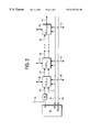
- FIG. 1 shows an ordering array 10 which may be configured to perform a variety of sorting functions.
- the sorting functions include a function for finding all integers less than a reference integer, a function for finding all integers greater than a reference integer, and a function for finding all integers equal to a reference integer.
- the sorting functions include a function for finding the maximum or minimum integer stored in the ordering array 10 .
- the ordering array 10 includes a set of logic cells (CELL 0,0 -CELL mx,my ).
- the logic cells CELL 0,0 -CELL mx,my are arranged as a set of rows 0-mx and a set of columns 0-my.
- the ordering array 10 receives a set of row inputs 20 - 22 (P 0,0 -P mx,0 and R 0,0 -R mx,0 ) and a set of column inputs 30 - 32 (V 0 -V my ) and provides a set of row outputs 40 - 42 (Q 0,0 -Q 0,my and S 0,0 -S 0,my ).
- the ordering array 10 may be implemented as an application specific integrated circuit (ASIC) or field programmable gate array (FPGA) in which the logic cells CELL 0,0 -CELL mx,my are programmed to perform a corresponding set of logic functions.
- ASIC application specific integrated circuit
- FPGA field programmable gate array
- the logic state of the CELL i,j is denoted K i,j .
- the ordering array 10 is configured to find which of the rows 0-mx stores an integer that is less than, greater than, or equal to a reference integer carried on the column inputs 30 - 32 .
- the following are the Boolean equations programmed into the ordering array 10 in this embodiment.
- the output conditions Q and S provided on the outputs 40 - 42 in this embodiment are defined as follows:
- the ordering array 10 is configured to find the minimum integer stored in the rows 0-mx.
- the following are the Boolean equations programmed into the ordering array 10 in this embodiment.
- the columns 1-my provide a logic function rather than an input function.
- V j [P 0,j ⁇ K 0,j + ⁇ overscore (P 0,j +L ) ⁇ ] ⁇ [ P 1,j ⁇ K 1,j + ⁇ overscore (P 1,j +L ) ⁇ ] ⁇ . . . ⁇ [ P my,j ⁇ K my,j + ⁇ overscore (P my,j +L ) ⁇ ]
- the function of the columns 1-my is an “AND” function of terms from each row 0-mx.
- This “AND” function may be implemented in an ASIC or FPGA using a “wired-OR” form with an open collector output of each cell to drive a vertical signal line in the ordering array 10 .
- the ordering array 10 is configured to find the maximum integer stored in the rows 0-mx.
- the following are the Boolean equations programmed into the ordering array 10 in this embodiment.
- the columns 1-my provide a logic function rather than an input function.
- V j [P 0,j ⁇ K 0,j ]+[P 1,j K 1,j ]+ . . . +[P my,j ⁇ K my,j ]
- the function of the columns 1-my is an “AND” function of terms from each row 0-mx.
- This “AND” function may be implemented in an ASIC or FPGA using a “wired-OR” form with an open collector output of each cell to drive a vertical signal line in the ordering array 10 .
- the ordering array 10 is configured to perform a particular one of the above functions using the equations given above. In other embodiments, the ordering array 10 may be programmed to perform multiple ones of the above functions. A global selection signal available to each CELL i,j may be used to select a particular function.
- the ordering array 10 may be employed in a variety of systems including systems having a processor that performs application-specific tasks.
- the ordering array 10 enables off loading of sorting tasks from the processor. For example, a processor may load the ordering array 10 with values to be sorted and then generate a next set of values to be sorted while the ordering array performs its sorting function.
- the output of the ordering array 10 may be supplied back to the processor that generated the values to be sorted or may be supplied to a different processor depending upon the particular application of the ordering array 10 .
- FIG. 2 shows circuitry for individually disabling the row 1 of the ordering array 10 . Similar circuitry may be implemented in the remaining rows 0,2-mx.
- An array enable signal 50 provides a chip select for the ordering array 10 while each of the rows 1-mx is individually enabled or disabled by setting a corresponding flip-flop such as a flip-flop 56 for the row 1.
- the Q output of the flip-flop 56 and the array enable signal 50 are combined by an AND gate 58 to provide an enable/disable signal 60 to the cells of the row 1.
- a row enable signal 52 is used to load the row 1 with an integer value and to set the flip-flop 56 thereby enabling the row 1.
- a row disable signal 54 is used to reset the flip-flop 56 which disables the row 1.
- FIG. 3 shows a motion control module 140 which includes an ordering device 102 that off-loads time consuming ordering tasks from a processor 100 .
- the motion control module 140 may be part of a motion control system which includes multiple motion control modules each of which controls motion along one or more axes of a device 130 .
- the motion control module 140 controls motion along an axis corresponding to an actuator 120 of the device 130 .
- the device 130 represents any type of device or any type of mechanical, electrical, chemical, or combination system. Examples are numerous and include printers, plotters, and manufacturing systems found in a wide variety of industries. The following discussion focuses on an example embodiment in which the device 130 is a plotter in which the actuator 120 controls the x position of a pen. It is apparent, however, that the teachings provided with respect to the example embodiment are readily applicable to a variety of other devices and systems including very complex systems with many more axes.
- the processor 100 generates a series of x control values to be applied to the actuator 120 according to a particular motion control function.
- the series of x control values to be applied to the actuator 120 may be computed by the processor 100 for predetermined t values.
- the ordering device 102 includes the ordering array 10 and an application array 110 .
- the application array 110 includes a row of cells corresponding to each row 0-mx of the ordering array 10 .
- the processor 100 stores the t values used to compute the series of x control values into the ordering array 10 and stores the x control values into corresponding rows of the application array 110 via a signal path 104 .
- the processor 100 may write the x control values and corresponding t values to the ordering device 102 in any order.
- the ordering array 10 is configured to find which of the rows 0-mx stores an integer that is less than, greater than, or equal to a reference integer carried on the column inputs 30 - 32 using the Boolean equations given above.
- the t values in the ordering array 10 provide the logic states K i,j .
- the output of a real-time clock 108 is applied to the column inputs 30 - 32 .
- the row outputs 40 - 42 indicate to logic in the application array 110 which of the rows 0-mx equals the value in the real-time clock 108 .
- the row of the application array 110 that corresponds to the row 0-mx of the ordering array 10 that equals the clock value on the column inputs 30 - 32 is read out to a digital-to-analog converter (DAC) 106 .
- the DAC 106 provides analog control signals to the actuator 120 .
- digital control values may be provided to the actuator 120 and the actuator 120 may include a DAC and signal processing circuitry.
- an ascending order of t values in the ordering array 10 match to the column inputs 30 - 32 and the x control values corresponding to the ascending order of t values are read out of the application array 110 and applied to the actuator 120 .
- Each matching row 1-mx may be individually disabled using circuitry described above.
- FIG. 4 shows an alternate embodiment of the ordering device 102 which drives a set of actuators 150 - 152 .
- the actuators 150 - 152 may drive the x and y axes, respectively, of a plotter device.
- one of the rows 0-mx of the ordering array 10 in this example row 0, is continuously loaded with clock values from the real-time clock 108 .
- the ordering array 10 is configured to find which of the rows 0-mx stores the minimum integer using the Boolean equations given above.
- An application array 160 stores control values for both of the actuators 150 - 152 .
- Control values for the actuator 150 are read out to a DAC 140 via channel A and control values for the actuator 152 are read out to a DAC 142 via channel B.
- the row 1 of the application array 160 stores a control value 170 , an indicator 180 that indicates that the control value 170 is for channel A, and includes a set of channel logic 190 for steering the control value 170 to the DAC 140 via channel A.
- the row 2 of the application array 160 stores a control value 172 , an indicator 182 that indicates that the control value 172 is for channel B, and includes a set of channel logic 192 for steering the control value 172 to the DAC 140 via channel A.
- each minimum row 1-mx triggers its corresponding channel logic in the application array 160 .
- Each minimum row 1-mx is disabled once being recognized as the minimum using circuitry described above.
- FIG. 5 shows an example implementation of the channel logic 190 .
- the channel logic in the rows 2-mx of the application array 160 may be implemented in a similar manner.
- the control value 170 is gated onto channel A or channel B with a pair of AND gates 202 - 204 .
- One or the other of the AND gates 202 - 204 is enabled by a selector circuit 200 . If the indicator 180 indicates channel A then the AND gate 202 is enabled. If the indicator 180 indicates channel B then the AND gate 204 is enabled.
- the selector circuit 200 is enabled by the outputs 41 which provide the row result from row 1 of the ordering array 10 and indicate whether row 1 holds the minimum integer in the ordering array 10 .
- the selector circuit 200 is enabled and the control value 170 is driven on channel A or B according to the indicator 180 .
- the row result 41 is combined with phase-2 of a clock signal 210 using an AND gate 206 to provide the row disable signal 54 for the row 1.
- the clock signal 210 is a 2 phase clock.
- Phase-1 of the clock signal 210 drives the real-time clock 108 .
- Phase-2 of the clock signal 210 clocks the control value for the recognized minimum of the rows 1-mx of the ordering array 10 onto channel A or B and then resets the minimum row before the next phase-1 starts another recognition sequence in the ordering array 10 .
- FIG. 6 shows circuitry in the channel logic of the application array 10 that may be employed in an embodiment in which more than one of the rows 1-mx may hold a minimum value.
- the channel logic 190 of the row 1 is substantially similar to that shown in FIG. 5 .
- Each of the remaining rows 2-mx includes circuitry substantially similar to the circuitry shown for the channel logic 192 .
- the channel logic 192 includes a pair of AND gates 290 - 292 that gate the control value 182 onto the channel A or B in response to a selector circuit 224 which takes as input the indicator 182 .
- An AND gate 286 provides a row disable signal 254 for the row 2.
- the generation of an enable signal 225 to the selector circuit 224 and the generation of the row disable signal 254 via the AND gate 286 is conditioned by a signal 249 .
- the signal 249 is a “daisy chain” signal from the previous row.
- the previous row to the channel logic 192 of the row 2 is the channel logic 190 of the row 1.
- the signal 249 is combined with a row result 241 for the row 2 by a gate 227 .
- the gate 227 provides the enable signal 225 to the selector circuit 224 and an input to the AND gate 286 .
- a daisy chain signal 250 to the next row, the row 3, is generated by combining the daisy chain signal 249 from the previous row, the row 1, with the row result 241 for the row 2 using an OR gate 230 .
- An ordering device may be used to generate a histogram.
- the ordering array is configured to find which of its rows are less than or equal to its column inputs and the application array sums the number of row result lines that indicate this criteria and clears the rows after recognition.
- An array of measured values is written to the ordering array.
- the value applied its column inputs are stepped in regular intervals defining the bin size for a histogram. The sum for each bin is generated by the application array.
- An ordering device may be used to execute code bodies using a time-script.
- One of the rows of the ordering array reflects a real-time clock value.
- the ordering array is configured to find the minimum value.
- the recognized row causes a value to be read out of the application array and passed as a parameter to an interrupt service routine. This enables time-scripts to be stored in the ordering device and the corresponding code bodies are called based upon the real-time clock value.
- An ordering device may be used to order alarms on a highest-priority-oldest-time-stamp-first basis.
- the ordering array includes two arrays. A left array holds priority values and a second array holds time stamp values.
- the left array is configured to find its maximum rows.
- the row results from the left array cause the second array to sort the maximum priority rows to find a minimum time-stamp value of the highest priority rows.
- the row recognition in the second array causes a value from the application array to be passed to an interrupt service routine.
- Incoming alarm or similar urgency based messages are written to the ordering device and the ordering array automatically orders them on a highest-priority-oldest-time-stamp-first basis.
- An ordering device may be used for periodic or aperiodic behaviors.
- One of the rows of the ordering array reflects a real-time clock value.
- the ordering array is configured to find the minimum value of a set of time-stamps.
- the recognized row causes a value to be read out of the application array and passed as a parameter to an interrupt service routine or to a DAC. This enables generation of arbitrary preprogrammed waveform or code execution sequences.
- Aperiodic behavior can be generated by varying the rate of the real-time clock row.
Landscapes
- Engineering & Computer Science (AREA)
- Physics & Mathematics (AREA)
- General Physics & Mathematics (AREA)
- Theoretical Computer Science (AREA)
- Computational Mathematics (AREA)
- Computing Systems (AREA)
- Mathematical Analysis (AREA)
- Mathematical Optimization (AREA)
- Pure & Applied Mathematics (AREA)
- General Engineering & Computer Science (AREA)
- Logic Circuits (AREA)
Priority Applications (2)
| Application Number | Priority Date | Filing Date | Title |
|---|---|---|---|
| US09/228,842 US6347324B1 (en) | 1999-01-12 | 1999-01-12 | Ordering devices |
| JP5927A JP2000207172A (ja) | 1999-01-12 | 2000-01-07 | 順序付け装置 |
Applications Claiming Priority (1)
| Application Number | Priority Date | Filing Date | Title |
|---|---|---|---|
| US09/228,842 US6347324B1 (en) | 1999-01-12 | 1999-01-12 | Ordering devices |
Publications (1)
| Publication Number | Publication Date |
|---|---|
| US6347324B1 true US6347324B1 (en) | 2002-02-12 |
Family
ID=22858767
Family Applications (1)
| Application Number | Title | Priority Date | Filing Date |
|---|---|---|---|
| US09/228,842 Expired - Fee Related US6347324B1 (en) | 1999-01-12 | 1999-01-12 | Ordering devices |
Country Status (2)
| Country | Link |
|---|---|
| US (1) | US6347324B1 (enExample) |
| JP (1) | JP2000207172A (enExample) |
Cited By (1)
| Publication number | Priority date | Publication date | Assignee | Title |
|---|---|---|---|---|
| US20160352388A1 (en) * | 2015-05-28 | 2016-12-01 | Qualcomm Incorporated | DC Power Line Synchronization for Automotive Sensors |
Citations (4)
| Publication number | Priority date | Publication date | Assignee | Title |
|---|---|---|---|---|
| US4604726A (en) * | 1983-04-18 | 1986-08-05 | Raytheon Company | Sorting apparatus |
| US4713786A (en) * | 1985-02-15 | 1987-12-15 | Harris Corporation | Digital hardware selection filter |
| US5122979A (en) * | 1989-05-31 | 1992-06-16 | Plessey Semiconductors Limited | Method and a digital electronic device for the evaluation of an extremum of a set of binary encoded data words |
| US5532948A (en) * | 1993-01-13 | 1996-07-02 | Sumitomo Metal Industries, Ltd. | Rank order filter |
-
1999
- 1999-01-12 US US09/228,842 patent/US6347324B1/en not_active Expired - Fee Related
-
2000
- 2000-01-07 JP JP5927A patent/JP2000207172A/ja active Pending
Patent Citations (4)
| Publication number | Priority date | Publication date | Assignee | Title |
|---|---|---|---|---|
| US4604726A (en) * | 1983-04-18 | 1986-08-05 | Raytheon Company | Sorting apparatus |
| US4713786A (en) * | 1985-02-15 | 1987-12-15 | Harris Corporation | Digital hardware selection filter |
| US5122979A (en) * | 1989-05-31 | 1992-06-16 | Plessey Semiconductors Limited | Method and a digital electronic device for the evaluation of an extremum of a set of binary encoded data words |
| US5532948A (en) * | 1993-01-13 | 1996-07-02 | Sumitomo Metal Industries, Ltd. | Rank order filter |
Cited By (2)
| Publication number | Priority date | Publication date | Assignee | Title |
|---|---|---|---|---|
| US20160352388A1 (en) * | 2015-05-28 | 2016-12-01 | Qualcomm Incorporated | DC Power Line Synchronization for Automotive Sensors |
| US9935685B2 (en) * | 2015-05-28 | 2018-04-03 | Qualcomm Incorporated | DC power line synchronization for automotive sensors |
Also Published As
| Publication number | Publication date |
|---|---|
| JP2000207172A (ja) | 2000-07-28 |
Similar Documents
| Publication | Publication Date | Title |
|---|---|---|
| US20240168718A1 (en) | Circuit based on digital domain in-memory computing | |
| US20230070387A1 (en) | Resistive random-access memory for exclusive nor (xnor) neural networks | |
| JP2671120B2 (ja) | データ処理セルおよびデータプロセッサ | |
| US11816595B2 (en) | Information processing system | |
| US5508636A (en) | Electronic system organised as an array of cells | |
| EP0096225A2 (en) | Interlaced programmable logic array having shared elements | |
| US5781769A (en) | Method and apparatus for using a content addressable memory for time tagged event processing | |
| EP3620911B1 (en) | Multiply-accumulate operation device, multiply-accumulate operation methods, and systems | |
| US6347324B1 (en) | Ordering devices | |
| US20240013850A1 (en) | Techniques for error mitigation to improve reliability for analog compute-in-memory | |
| TWI709910B (zh) | 處理資料之處理器及方法 | |
| Zahedi et al. | Tile architecture and hardware implementation for computation-in-memory | |
| US3932845A (en) | Specialized digital computer with divided memory and arithmetic units | |
| US5479572A (en) | Artificial neural network (ANN) classifier apparatus for selecting related computer routines and methods | |
| EP0806007B1 (en) | A parametrizable control module comprising first and second loadables counters, an electronic circuit comprising a plurality of such parametrized control modules, and a method for synthesizing such circuit | |
| US5274589A (en) | Method and apparatus for writing and reading data to/from a memory | |
| US5572198A (en) | Method and apparatus for routing in reduced switch matrices to provide one hundred percent coverage | |
| EP0479919A1 (en) | Method and circuit for programmable element sequence selection | |
| US4766532A (en) | Sequential array logic | |
| EP0662691B1 (en) | Count unit for non volatile memories | |
| US4764895A (en) | Data processor for changing the sequential format of inputted records | |
| US20230009922A1 (en) | Decoupled Execution Of Workload For Crossbar Arrays | |
| Hoffmann et al. | Implementation of the Massively Parallel Model GCA | |
| RU2153699C1 (ru) | Устройство для перераспределения задач между процессорами | |
| EP0592523B1 (en) | Bookkeeping memory |
Legal Events
| Date | Code | Title | Description |
|---|---|---|---|
| AS | Assignment |
Owner name: HEWLETT-PACKARD COMPANY, CALIFORNIA Free format text: ASSIGNMENT OF ASSIGNORS INTEREST;ASSIGNOR:EIDSON JOHN C.;REEL/FRAME:009796/0288 Effective date: 19990224 |
|
| AS | Assignment |
Owner name: HEWLETT-PACKARD COMPANY, COLORADO Free format text: MERGER;ASSIGNOR:HEWLETT-PACKARD COMPANY;REEL/FRAME:010759/0049 Effective date: 19980520 |
|
| AS | Assignment |
Owner name: AGILENT TECHNOLOGIES INC, CALIFORNIA Free format text: ASSIGNMENT OF ASSIGNORS INTEREST;ASSIGNOR:HEWLETT-PACKARD COMPANY;REEL/FRAME:010977/0540 Effective date: 19991101 |
|
| FPAY | Fee payment |
Year of fee payment: 4 |
|
| REMI | Maintenance fee reminder mailed | ||
| LAPS | Lapse for failure to pay maintenance fees | ||
| STCH | Information on status: patent discontinuation |
Free format text: PATENT EXPIRED DUE TO NONPAYMENT OF MAINTENANCE FEES UNDER 37 CFR 1.362 |
|
| FP | Lapsed due to failure to pay maintenance fee |
Effective date: 20100212 |