US6288917B1 - Three stage power conditioning circuit - Google Patents
Three stage power conditioning circuit Download PDFInfo
- Publication number
- US6288917B1 US6288917B1 US09/456,101 US45610199A US6288917B1 US 6288917 B1 US6288917 B1 US 6288917B1 US 45610199 A US45610199 A US 45610199A US 6288917 B1 US6288917 B1 US 6288917B1
- Authority
- US
- United States
- Prior art keywords
- inductor
- coupled
- stage
- conductor
- power
- Prior art date
- Legal status (The legal status is an assumption and is not a legal conclusion. Google has not performed a legal analysis and makes no representation as to the accuracy of the status listed.)
- Expired - Lifetime
Links
Images
Classifications
-
- H—ELECTRICITY
- H02—GENERATION; CONVERSION OR DISTRIBUTION OF ELECTRIC POWER
- H02H—EMERGENCY PROTECTIVE CIRCUIT ARRANGEMENTS
- H02H9/00—Emergency protective circuit arrangements for limiting excess current or voltage without disconnection
- H02H9/04—Emergency protective circuit arrangements for limiting excess current or voltage without disconnection responsive to excess voltage
-
- H—ELECTRICITY
- H03—ELECTRONIC CIRCUITRY
- H03H—IMPEDANCE NETWORKS, e.g. RESONANT CIRCUITS; RESONATORS
- H03H7/00—Multiple-port networks comprising only passive electrical elements as network components
- H03H7/01—Frequency selective two-port networks
- H03H7/03—Frequency selective two-port networks comprising means for compensation of loss
-
- H—ELECTRICITY
- H02—GENERATION; CONVERSION OR DISTRIBUTION OF ELECTRIC POWER
- H02H—EMERGENCY PROTECTIVE CIRCUIT ARRANGEMENTS
- H02H9/00—Emergency protective circuit arrangements for limiting excess current or voltage without disconnection
- H02H9/005—Emergency protective circuit arrangements for limiting excess current or voltage without disconnection avoiding undesired transient conditions
-
- H—ELECTRICITY
- H03—ELECTRONIC CIRCUITRY
- H03H—IMPEDANCE NETWORKS, e.g. RESONANT CIRCUITS; RESONATORS
- H03H7/00—Multiple-port networks comprising only passive electrical elements as network components
- H03H7/42—Networks for transforming balanced signals into unbalanced signals and vice versa, e.g. baluns
- H03H7/425—Balance-balance networks
- H03H7/427—Common-mode filters
-
- H—ELECTRICITY
- H02—GENERATION; CONVERSION OR DISTRIBUTION OF ELECTRIC POWER
- H02H—EMERGENCY PROTECTIVE CIRCUIT ARRANGEMENTS
- H02H9/00—Emergency protective circuit arrangements for limiting excess current or voltage without disconnection
- H02H9/04—Emergency protective circuit arrangements for limiting excess current or voltage without disconnection responsive to excess voltage
- H02H9/042—Emergency protective circuit arrangements for limiting excess current or voltage without disconnection responsive to excess voltage comprising means to limit the absorbed power or indicate damaged over-voltage protection device
-
- H—ELECTRICITY
- H03—ELECTRONIC CIRCUITRY
- H03H—IMPEDANCE NETWORKS, e.g. RESONANT CIRCUITS; RESONATORS
- H03H7/00—Multiple-port networks comprising only passive electrical elements as network components
- H03H7/01—Frequency selective two-port networks
- H03H7/0107—Non-linear filters
Definitions
- the present invention relates generally to power conditioning circuits, and more particularly, to power conditioning circuits that protect attached load equipment from voltage and current surges due to, for example, lightning strikes or other power disturbances.
- Power conditioning circuits have long been used to protect sensitive load equipment from transients caused by lightning strikes, noise and other power line disturbances.
- filter elements are used in the line and neutral conductors which trap and/or shunt unwanted power frequencies away from the load. See, for example, Speet et al. U.S. Pat. No. 4,814,941 and Taylor et al. U.S. Pat. No. 5,490,030.
- Muelleman U.S. Pat. No. 5,448,443 discloses a power conditioning device and method including an isolation transformer having primary and secondary sides and a ground impedance connected between the secondary side of the isolation transformer at a safety ground and an earth ground.
- the Muelleman device prevents ground current loops by redirecting transient ground currents to neutral, but does not provide current limiting or noise suppression.
- a power conditioning circuit is simple in design, yet effective to limit damaging transients.
- a power conditioning circuit for conditioning power supplied by a power source at a nominal frequency over line, neutral and ground conductors to first, second and third output lines, respectively, includes a first, second and third stage.
- the first stage is connected to the line, neutral and ground conductors, and is adapted to provide voltage suppression.
- the second stage is connected to the first stage, and includes first, second and third inductors coupled in series between the line, neutral and ground conductors, respectively, and the first, second and third output lines, respectively, and all of the power supplied by the power source to the first, second and third output lines flows through the first, second and third inductors.
- Each of the inductors block power at frequencies greater than the nominal frequency thereby to prevent power at frequencies greater than the nominal frequency from reaching the first, second and third output lines.
- the third stage is connected to the second stage and is further connected to the first, second and third output lines and is adapted to provide voltage suppression and voltage clamping.
- the first stage includes first, second and third metal oxide varistors.
- the first metal oxide varistor is coupled between the line conductor and the neutral conductor and the second metal oxide varistor is coupled between the line conductor and the ground conductor and the third metal oxide varistor is coupled between the neutral conductor and the ground conductor.
- the first stage includes a capacitor coupled between the neutral conductor and the ground conductor.
- the third stage includes a first metal oxide varistor, wherein the first metal oxide varistor is coupled between the neutral conductor and the ground conductor.
- the third stage may further include a second metal oxide varistor, wherein the second metal oxide varistor is coupled between the line conductor and the neutral conductor.
- the third stage includes first and second diodes coupled in anti-parallel relationship across the neutral conductor and the ground conductor.
- the third stage may further include a capacitor coupled between the neutral conductor and the ground conductor.
- the first, second and third inductors are common mode inductors each having a core and a set of first and second windings.
- the first inductor is coupled between the line conductor and the first output line via the first winding of the first inductor and the first inductor is further coupled between the neutral conductor and the second output line via the second winding of the first inductor and the first and second windings of the first inductor are wound around the core of the first inductor.
- the second inductor is coupled between the neutral conductor and the second output line via the first winding of the second inductor and the second inductor is further coupled between the ground conductor and the third output line via the second winding of the second inductor and the first and second windings of the second inductor are wound around the core of the second inductor.
- the third inductor is coupled between the ground conductor and the third output line via the first winding of the third inductor and the third inductor is further coupled between the line conductor and the first output line via the second winding of the third inductor and the first and second windings of the third inductor are wound around the core of the third inductor.
- the first, second and third output lines of the power conditioning circuit of the present invention may be coupled to a load having a capacitive impedance and the first, second and third inductors may be rated to compensate for the capacitive impedance of the load.
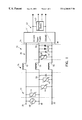
- FIG. 1 comprises a schematic diagram of a first embodiment of the present invention.
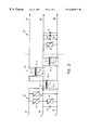
- FIG. 2 comprises a schematic diagram of a second embodiment of the present invention.
- a power conditioning circuit 20 having a set of first, second and third stages 22 , 24 and 26 is connected between a set of line, neutral and ground conductors 28 , 30 , 32 and a set of output lines 34 , 36 , 38 .
- the line, neutral and ground conductors 28 , 30 , 32 may be connected to a commercial source of power 40 or any other power source.
- the first, second and third stages 22 , 24 and 26 are arranged such that power entering the power conditioning circuit from the power source 40 first flows through the first stage, then through the second stage and lastly the third stage. Upon exiting the third stage, the power reaches the output lines 34 , 36 and 38 which are connected to the load(s) 42 .
- the load(s) 42 may include, for example, a power supply 41 that is coupled to an electronic device 43 , such as a computer.
- the first stage 22 includes first, second and third metal oxide varistors (MOVs) 44 , 46 and 48 connected across the line and neutral conductors 28 , 30 , the line and ground conductors 28 , 32 and the neutral and ground conductors 30 , 32 , respectively.
- MOVs metal oxide varistors
- a first capacitor 50 that preferably, although not necessarily, has a rating of 25 microfarads is connected across the neutral and ground conductors 30 , 32 .
- the second stage 24 includes first, second and third inductors 52 , 54 , 56 connected in series on each of the line, neutral and ground conductors 28 , 30 and 32 , respectively.
- the third stage 26 includes a fourth MOV 60 connected between neutral and ground conductors 30 and 32 .
- a second capacitor 62 is coupled between neutral and ground conductors 30 , 32 and first and second rectifier diodes 64 , 66 are connected in anti-parallel relationship between the neutral and ground lines.
- the first, second and third MOVs 44 , 46 , 48 of the first stage 22 limit the voltage magnitudes appearing across the line, neutral and ground conductors 28 , 30 , 32 by shunting currents during voltage spikes that exceed a threshold voltage. It is preferable, although not necessary, that the first, second and third MOV's each have a rating of 150 volts RMS.
- the first, second, and third inductors 52 , 54 and 56 have rating values that attenuate transients having one or more frequency components in excess of the nominal frequency (typically 60 Hz) of the power supplied via the line, neutral and ground conductors 22 , 24 , 26 . It is preferable, although not necessary, that the inductors 52 , 54 and 56 each have the rating of 5 millihenries (mh).
- the third stage 26 suppresses substantially all undesired remaining energy components that are not diverted or attenuated by the first and second stages 22 , 24 .
- the fourth MOV 60 limits the magnitude of the voltages appearing on the neutral and/or ground conductors 30 and 32 by shunting currents to ground. Because any high energy surges and high energy surge components have ideally been filtered by the first and second stages, the elements of the third stage need only be rated to divert or attenuate lower energy surges. As a result, the MOV 60 preferably, although not necessarily, has a rating of 140 V RMS.
- the second capacitor 62 which operates to shunt power components having undesired frequencies to the ground conductor 32 , preferably, although not necessarily, has a rating of 25 microfarads.
- the first and second rectifier diodes 64 and 66 are connected in parallel between the neutral and ground conductors 30 , 32 such that the polarity of the first rectifier diode 64 opposes the polarity of the second rectifier diode 66 . Arranging the rectifier diodes 64 , 66 in this manner enables precise, low level voltage clamping, thereby further enabling voltage control for the load ground. In applications wherein the electronic device 43 of the load 42 is a computer, low level voltage clamping on the ground leg is especially advantageous because the ground lead attaches directly to the microprocessor and is, therefore, a potential source of damaging voltage spikes.
- the first, second and third inductors 52 , 54 , 56 of the second stage are preferably sized not only to dampen, or suppress high frequency spikes, but also to offset the capacitive impedance characteristics of the load.
- inductors 52 , 54 and 56 having rating values that improve the overall power factor of the power supplied by the conditioning circuit to the capacitive load, i.e., it is desirable to obtain a power factor that approximates unity or comes as close thereto as practical.
- the three stage power conditioning circuit described herein provides high quality, precise and yet inexpensive power conditioning. More particularly, by arranging the first, second and third stages 22 , 24 , 26 in a cascaded order such that the first and second stages 22 and 24 effect high energy suppression and isolation and the third stage 26 effects low energy transient noise suppression, less expensive circuit elements may be employed in each of the three stages.
- the cost savings achieved by way of the three stage power conditioning circuit of the present invention are best understood with reference to the rating of each of the circuit elements and a manufacturer specified tolerance level associated with each of the ratings. Specifically, the rating and tolerance level associated with each circuit element affects the cost of the circuit element such that circuit elements that are rated for higher voltage levels and/or current levels are typically more costly than circuit elements rated to handle lower levels.
- a circuit element having a wide tolerance associated with the rating is typically less precise and therefore less costly than a circuit element having a narrower, and thus, more precise tolerance associated with the rating.
- the first and second stages 22 , 24 are used to suppress and/or attenuate high energy transients and as a result the circuit elements of the first and second stages 22 , 24 are preferably rated to handle these high energy surges.
- the circuit elements of the first and second stages 22 , 24 need not be particularly precise and thus may have ratings with a wider tolerance level than would otherwise be effective to adequately protect the attached loads.
- the increased cost of providing circuit elements in the first and second stages 22 , 24 that are capable of handling high energy surges is offset by the wider tolerance levels associated with the ratings.
- circuit elements having narrower tolerance levels are desirable.
- the increased cost associated with a narrower tolerance level is offset by the decreased cost of the lower ratings associated with the circuit elements of the third stage 26 .
- the second stage of the three stage power conditioning circuit may be modified to include common mode inductors 70 , 72 , 74 each having a first winding 70 - 1 , 72 - 1 and 74 - 1 respectively, a second winding 70 - 2 , 72 - 2 and 74 - 2 respectively, and a core 70 - 3 , 72 - 3 and 74 - 3 , respectively.
- the first winding 70 - 1 of the common mode inductor 70 is coupled in series with the first winding 74 - 1 of the common mode inductor 74 between line conductor 28 and the first output line 34
- the second winding 70 - 2 of the common mode inductor 70 is coupled in series between the neutral conductor 30 and the second output line 36
- the second windings 72 - 2 and 74 - 2 of the common mode inductors 72 , 74 are coupled in series between the ground conductor 32 and the third output line 38 .
- the first and second windings 70 - 1 and 70 - 2 are wound on the core 70 - 3 while the first and second windings 72 - 1 and 72 - 2 are wound on the core 72 - 3 and the first and second windings 74 - 1 and 74 - 2 are wound on the core 74 - 3 .
- Each of the common mode inductors 70 , 72 and 74 are arranged such that the polarity of the windings of each of the inductors 70 , 72 and 74 is identically aligned as indicated by the polarity dots shown beside each of the inductors 70 , 72 and 74 .
- the third stage of the power conditioning circuit may include an additional MOV (not shown) connected to the line conductor at a point between the line conductor 28 and the output line 34 and coupled between the line conductor 28 and the neutral conductor 30 to protect against a high power energy surge that reaches the third stage.
- an additional MOV (not shown) connected to the line conductor at a point between the line conductor 28 and the output line 34 and coupled between the line conductor 28 and the neutral conductor 30 to protect against a high power energy surge that reaches the third stage.
Landscapes
- Emergency Protection Circuit Devices (AREA)
- Power Conversion In General (AREA)
Priority Applications (8)
| Application Number | Priority Date | Filing Date | Title |
|---|---|---|---|
| US09/456,101 US6288917B1 (en) | 1998-01-20 | 1999-12-06 | Three stage power conditioning circuit |
| EP00978604A EP1236260A1 (fr) | 1999-12-06 | 2000-11-14 | Dispositif de conditionnement d'energie a trois etages |
| AU16054/01A AU756806B2 (en) | 1999-12-06 | 2000-11-14 | A three stage power conditioning circuit |
| JP2001542439A JP2003516103A (ja) | 1999-12-06 | 2000-11-14 | 三段式電力調節回路 |
| KR1020027007185A KR20020067913A (ko) | 1999-12-06 | 2000-11-14 | 3단 전력 조절회로 |
| PCT/US2000/031199 WO2001041278A1 (fr) | 1999-12-06 | 2000-11-14 | Dispositif de conditionnement d'energie a trois etages |
| CA002394853A CA2394853C (fr) | 1999-12-06 | 2000-11-14 | Dispositif de conditionnement d'energie a trois etages |
| TW089124532A TW490905B (en) | 1999-12-06 | 2000-11-20 | A three stage power conditioning circuit |
Applications Claiming Priority (2)
| Application Number | Priority Date | Filing Date | Title |
|---|---|---|---|
| US09/009,210 US6166458A (en) | 1998-01-20 | 1998-01-20 | Power conditioning circuit |
| US09/456,101 US6288917B1 (en) | 1998-01-20 | 1999-12-06 | Three stage power conditioning circuit |
Related Parent Applications (1)
| Application Number | Title | Priority Date | Filing Date |
|---|---|---|---|
| US09/009,210 Continuation-In-Part US6166458A (en) | 1998-01-20 | 1998-01-20 | Power conditioning circuit |
Publications (1)
| Publication Number | Publication Date |
|---|---|
| US6288917B1 true US6288917B1 (en) | 2001-09-11 |
Family
ID=23811429
Family Applications (1)
| Application Number | Title | Priority Date | Filing Date |
|---|---|---|---|
| US09/456,101 Expired - Lifetime US6288917B1 (en) | 1998-01-20 | 1999-12-06 | Three stage power conditioning circuit |
Country Status (8)
| Country | Link |
|---|---|
| US (1) | US6288917B1 (fr) |
| EP (1) | EP1236260A1 (fr) |
| JP (1) | JP2003516103A (fr) |
| KR (1) | KR20020067913A (fr) |
| AU (1) | AU756806B2 (fr) |
| CA (1) | CA2394853C (fr) |
| TW (1) | TW490905B (fr) |
| WO (1) | WO2001041278A1 (fr) |
Cited By (14)
| Publication number | Priority date | Publication date | Assignee | Title |
|---|---|---|---|---|
| US20040218407A1 (en) * | 2003-01-17 | 2004-11-04 | Matsushita Electric Works, Ltd. | Switching power supply device |
| US6911777B1 (en) * | 2003-08-14 | 2005-06-28 | Cooper Industries, Inc. | Clamp-on low power isolation transformer for airfield lighting |
| US20070103165A1 (en) * | 2005-11-10 | 2007-05-10 | Magicground Technology, Llc | Ground testing method and apparatus |
| US20080025053A1 (en) * | 2006-07-25 | 2008-01-31 | Januszewski Michael W | Uninterruptible power supply with transient suppression |
| US20090207540A1 (en) * | 2008-02-14 | 2009-08-20 | Primax Electronics Ltd. | Power strip having surge protective circuit |
| US20090243758A1 (en) * | 2008-03-14 | 2009-10-01 | Januszewski Michael W | Power conditioning circuit utilizing high oersted rating inductors |
| US20110181994A1 (en) * | 2010-01-27 | 2011-07-28 | Shun-An Liao | Surge energy transfer circuit |
| CN102142678A (zh) * | 2010-02-03 | 2011-08-03 | 廖顺安 | 突波能量转换电路 |
| CN102170119A (zh) * | 2010-10-20 | 2011-08-31 | 南京信息工程大学 | 一种含有lc退耦元件的组合式电涌保护器 |
| US20110279935A1 (en) * | 2009-01-29 | 2011-11-17 | Panasonic Corporation | Differential transmission circuit and electronic device provided with the same |
| US20170005469A1 (en) * | 2014-06-11 | 2017-01-05 | 540 Grid Solutions, Llc | Surge suppression system for medium and high voltage |
| CN113381593A (zh) * | 2021-06-29 | 2021-09-10 | 杭州米福科技有限公司 | 一种大功率容性负载仪器的前端辅助电路 |
| US11923664B2 (en) | 2022-01-10 | 2024-03-05 | Dell Products L.P. | Power line filtering at equipment rack and module levels |
| EP4475413A1 (fr) * | 2023-06-09 | 2024-12-11 | Bilancio LLC | Appareil de redressement électromagnétique et procédé d'atténuation des harmoniques à partir d'un neutre dans un circuit à courant alternatif |
Families Citing this family (3)
| Publication number | Priority date | Publication date | Assignee | Title |
|---|---|---|---|---|
| CA2647813A1 (fr) * | 2006-03-31 | 2007-10-18 | Leveler Llc | Circuits de conditionnement d'alimentation polyphasee |
| TWM332325U (en) * | 2007-10-30 | 2008-05-11 | Anmax Lightning Technology Corp | Refined structure of series surge suppression |
| EP3340410B1 (fr) * | 2016-12-22 | 2020-10-28 | ABB Schweiz AG | Protection d'un élément inductif |
Citations (20)
| Publication number | Priority date | Publication date | Assignee | Title |
|---|---|---|---|---|
| US4429338A (en) | 1979-07-11 | 1984-01-31 | Siemens Aktiengesellschaft | Earth contact monitoring device for a polyphase three-phase filter circuit |
| US4703386A (en) | 1984-06-08 | 1987-10-27 | Steelcase, Inc. | Power receptacle and associated filter |
| US4802055A (en) | 1987-10-26 | 1989-01-31 | Joseph L. Brooks Manufacturing Corp. | Transient voltage surge suppressor |
| US4814941A (en) | 1984-06-08 | 1989-03-21 | Steelcase Inc. | Power receptacle and nested line conditioner arrangement |
| US4868732A (en) | 1987-10-28 | 1989-09-19 | International Business Machines Corporation | Pluggable power system having magnetic flux coupled power transformer and inductive filter components |
| US4901183A (en) | 1988-08-29 | 1990-02-13 | World Products, Inc. | Surge protection device |
| US4999729A (en) | 1989-08-09 | 1991-03-12 | Stifter Francis J | Satellite receiver protection apparatus |
| US5105327A (en) | 1990-05-10 | 1992-04-14 | Uses, Inc. | Ac power conditioning circuit |
| US5162963A (en) | 1989-03-14 | 1992-11-10 | Hughes Aircraft Company | Surge eliminator for switching converters |
| US5287288A (en) | 1992-10-30 | 1994-02-15 | Electric Power Research Institute, Inc. | Active power line conditioner with low cost surge protection and fast overload recovery |
| US5355025A (en) | 1992-10-30 | 1994-10-11 | Electric Power Research Institute, Inc. | Active power line conditioner with synchronous transformation control |
| US5448443A (en) | 1992-07-29 | 1995-09-05 | Suvon Associates | Power conditioning device and method |
| US5465203A (en) | 1993-06-18 | 1995-11-07 | Electric Power Research Institute, Inc. | Hybrid series active/parallel passive power line conditioner with controlled harmonic injection |
| US5490030A (en) | 1994-01-31 | 1996-02-06 | Taylor; Harold L. | Electromagnetic and radio frequency interference suppression for ground fault circuit interrupters |
| WO1996039735A1 (fr) | 1995-06-05 | 1996-12-12 | Powervar, Inc. | Conditionnement sans transformateur d'un reseau de distribution d'energie |
| US5589718A (en) | 1995-04-14 | 1996-12-31 | Monster Cable International, Ltd. | Power line conditioner |
| US5617284A (en) | 1994-08-05 | 1997-04-01 | Paradise; Rick | Power surge protection apparatus and method |
| US5731965A (en) * | 1996-06-21 | 1998-03-24 | Wisconsin Alumni Research Foundation | Power line harmonic reduction by hybrid parallel active/passive filter system with square wave inverter and DC bus control |
| US5757099A (en) * | 1996-03-01 | 1998-05-26 | Wisconsin Alumni Research Foundation | Hybrid parallel active/passive filter system with dynamically variable inductance |
| WO1999037007A1 (fr) | 1998-01-20 | 1999-07-22 | Leveler | Circuit de conditionnement d'energie |
-
1999
- 1999-12-06 US US09/456,101 patent/US6288917B1/en not_active Expired - Lifetime
-
2000
- 2000-11-14 WO PCT/US2000/031199 patent/WO2001041278A1/fr not_active Ceased
- 2000-11-14 KR KR1020027007185A patent/KR20020067913A/ko not_active Ceased
- 2000-11-14 CA CA002394853A patent/CA2394853C/fr not_active Expired - Fee Related
- 2000-11-14 AU AU16054/01A patent/AU756806B2/en not_active Ceased
- 2000-11-14 EP EP00978604A patent/EP1236260A1/fr not_active Ceased
- 2000-11-14 JP JP2001542439A patent/JP2003516103A/ja active Pending
- 2000-11-20 TW TW089124532A patent/TW490905B/zh not_active IP Right Cessation
Patent Citations (21)
| Publication number | Priority date | Publication date | Assignee | Title |
|---|---|---|---|---|
| US4429338A (en) | 1979-07-11 | 1984-01-31 | Siemens Aktiengesellschaft | Earth contact monitoring device for a polyphase three-phase filter circuit |
| US4703386A (en) | 1984-06-08 | 1987-10-27 | Steelcase, Inc. | Power receptacle and associated filter |
| US4814941A (en) | 1984-06-08 | 1989-03-21 | Steelcase Inc. | Power receptacle and nested line conditioner arrangement |
| US4802055A (en) | 1987-10-26 | 1989-01-31 | Joseph L. Brooks Manufacturing Corp. | Transient voltage surge suppressor |
| US4868732A (en) | 1987-10-28 | 1989-09-19 | International Business Machines Corporation | Pluggable power system having magnetic flux coupled power transformer and inductive filter components |
| US4901183A (en) | 1988-08-29 | 1990-02-13 | World Products, Inc. | Surge protection device |
| US5162963A (en) | 1989-03-14 | 1992-11-10 | Hughes Aircraft Company | Surge eliminator for switching converters |
| US4999729A (en) | 1989-08-09 | 1991-03-12 | Stifter Francis J | Satellite receiver protection apparatus |
| US5105327A (en) | 1990-05-10 | 1992-04-14 | Uses, Inc. | Ac power conditioning circuit |
| US5448443A (en) | 1992-07-29 | 1995-09-05 | Suvon Associates | Power conditioning device and method |
| US5355025A (en) | 1992-10-30 | 1994-10-11 | Electric Power Research Institute, Inc. | Active power line conditioner with synchronous transformation control |
| US5287288A (en) | 1992-10-30 | 1994-02-15 | Electric Power Research Institute, Inc. | Active power line conditioner with low cost surge protection and fast overload recovery |
| US5465203A (en) | 1993-06-18 | 1995-11-07 | Electric Power Research Institute, Inc. | Hybrid series active/parallel passive power line conditioner with controlled harmonic injection |
| US5490030A (en) | 1994-01-31 | 1996-02-06 | Taylor; Harold L. | Electromagnetic and radio frequency interference suppression for ground fault circuit interrupters |
| US5617284A (en) | 1994-08-05 | 1997-04-01 | Paradise; Rick | Power surge protection apparatus and method |
| US5589718A (en) | 1995-04-14 | 1996-12-31 | Monster Cable International, Ltd. | Power line conditioner |
| WO1996039735A1 (fr) | 1995-06-05 | 1996-12-12 | Powervar, Inc. | Conditionnement sans transformateur d'un reseau de distribution d'energie |
| US5757099A (en) * | 1996-03-01 | 1998-05-26 | Wisconsin Alumni Research Foundation | Hybrid parallel active/passive filter system with dynamically variable inductance |
| US5731965A (en) * | 1996-06-21 | 1998-03-24 | Wisconsin Alumni Research Foundation | Power line harmonic reduction by hybrid parallel active/passive filter system with square wave inverter and DC bus control |
| WO1999037007A1 (fr) | 1998-01-20 | 1999-07-22 | Leveler | Circuit de conditionnement d'energie |
| US6166458A (en) * | 1998-01-20 | 2000-12-26 | Leveler | Power conditioning circuit |
Cited By (37)
| Publication number | Priority date | Publication date | Assignee | Title |
|---|---|---|---|---|
| US7088596B2 (en) * | 2003-01-17 | 2006-08-08 | Matsushita Electric Works, Ltd. | Switching power supply with novel common mode filter arrangement |
| US20040218407A1 (en) * | 2003-01-17 | 2004-11-04 | Matsushita Electric Works, Ltd. | Switching power supply device |
| US6911777B1 (en) * | 2003-08-14 | 2005-06-28 | Cooper Industries, Inc. | Clamp-on low power isolation transformer for airfield lighting |
| US20070103165A1 (en) * | 2005-11-10 | 2007-05-10 | Magicground Technology, Llc | Ground testing method and apparatus |
| US7323878B2 (en) * | 2005-11-10 | 2008-01-29 | Magicground Technology Llc | Ground testing method and apparatus |
| US20080025053A1 (en) * | 2006-07-25 | 2008-01-31 | Januszewski Michael W | Uninterruptible power supply with transient suppression |
| WO2009014743A1 (fr) * | 2007-07-25 | 2009-01-29 | Leveler Llc | Alimentation électrique ininterruptible avec suppression des transitoires |
| US8004811B2 (en) * | 2008-02-14 | 2011-08-23 | Primax Electronics Ltd. | Power strip having surge protective circuit |
| US20090207540A1 (en) * | 2008-02-14 | 2009-08-20 | Primax Electronics Ltd. | Power strip having surge protective circuit |
| US20090243758A1 (en) * | 2008-03-14 | 2009-10-01 | Januszewski Michael W | Power conditioning circuit utilizing high oersted rating inductors |
| US8223468B2 (en) * | 2008-03-14 | 2012-07-17 | Leveler Llc | Power conditioning circuit utilizing high oersted rating inductors |
| US20110279935A1 (en) * | 2009-01-29 | 2011-11-17 | Panasonic Corporation | Differential transmission circuit and electronic device provided with the same |
| US8693151B2 (en) * | 2009-01-29 | 2014-04-08 | Panasonic Corporation | Differential transmission circuit and electronic device provided with the same |
| US20110181994A1 (en) * | 2010-01-27 | 2011-07-28 | Shun-An Liao | Surge energy transfer circuit |
| US8295024B2 (en) * | 2010-01-27 | 2012-10-23 | Shun-An Liao | Surge energy transfer circuit |
| CN102142678A (zh) * | 2010-02-03 | 2011-08-03 | 廖顺安 | 突波能量转换电路 |
| CN102142678B (zh) * | 2010-02-03 | 2014-05-07 | 廖顺安 | 突波能量转换电路 |
| CN102170119A (zh) * | 2010-10-20 | 2011-08-31 | 南京信息工程大学 | 一种含有lc退耦元件的组合式电涌保护器 |
| US20170005469A1 (en) * | 2014-06-11 | 2017-01-05 | 540 Grid Solutions, Llc | Surge suppression system for medium and high voltage |
| US10312689B2 (en) | 2014-06-11 | 2019-06-04 | Asator Global Technologies Llc | Surge suppression system for medium and high voltage |
| US10312686B2 (en) | 2014-06-11 | 2019-06-04 | Asator Global Technologies Llc | Surge suppression system for medium and high voltage |
| US10312690B2 (en) | 2014-06-11 | 2019-06-04 | Asator Global Technologies Llc | Surge suppression system for medium and high voltage |
| US10312688B2 (en) | 2014-06-11 | 2019-06-04 | Asator Global Technologies Llc | Surge suppression system for medium and high voltage |
| US10312691B2 (en) | 2014-06-11 | 2019-06-04 | Asator Global Technologies Llc | Surge suppression system for medium and high voltage |
| US10312687B2 (en) | 2014-06-11 | 2019-06-04 | Asator Global Technologies Llc | Surge suppression system for medium and high voltage |
| US10326273B2 (en) | 2014-06-11 | 2019-06-18 | Asator Global Technologies Llc | Surge suppression system for medium and high voltage |
| US10396558B2 (en) * | 2014-06-11 | 2019-08-27 | Asator Global Technologies Llc | Surge suppression system for medium and high voltage |
| US10404068B2 (en) | 2014-06-11 | 2019-09-03 | Asator Global Technologies Llc | Surge suppression system for medium and high voltage |
| US10424927B2 (en) * | 2014-06-11 | 2019-09-24 | Asator Global Technologies Llc | Surge suppression system for medium and high voltage |
| US10431982B2 (en) | 2014-06-11 | 2019-10-01 | Asator Global Technologies Llc | Surge suppression system for medium and high voltage |
| US10431981B2 (en) | 2014-06-11 | 2019-10-01 | Asator Global Technologies Llc | Surge suppression system for medium and high voltage |
| US10439397B2 (en) | 2014-06-11 | 2019-10-08 | Asator Global Technologies Llc | Surge suppression system for medium and high voltage |
| US10439395B2 (en) | 2014-06-11 | 2019-10-08 | Asator Global Technologies Llc | Surge suppression system for medium and high voltage |
| US10439396B2 (en) | 2014-06-11 | 2019-10-08 | Asator Global Technologies Llc | Surge suppression system for medium and high voltage |
| CN113381593A (zh) * | 2021-06-29 | 2021-09-10 | 杭州米福科技有限公司 | 一种大功率容性负载仪器的前端辅助电路 |
| US11923664B2 (en) | 2022-01-10 | 2024-03-05 | Dell Products L.P. | Power line filtering at equipment rack and module levels |
| EP4475413A1 (fr) * | 2023-06-09 | 2024-12-11 | Bilancio LLC | Appareil de redressement électromagnétique et procédé d'atténuation des harmoniques à partir d'un neutre dans un circuit à courant alternatif |
Also Published As
| Publication number | Publication date |
|---|---|
| AU1605401A (en) | 2001-06-12 |
| JP2003516103A (ja) | 2003-05-07 |
| CA2394853A1 (fr) | 2001-06-07 |
| CA2394853C (fr) | 2007-07-03 |
| EP1236260A1 (fr) | 2002-09-04 |
| TW490905B (en) | 2002-06-11 |
| AU756806B2 (en) | 2003-01-23 |
| WO2001041278A1 (fr) | 2001-06-07 |
| KR20020067913A (ko) | 2002-08-24 |
Similar Documents
| Publication | Publication Date | Title |
|---|---|---|
| CA2394853C (fr) | Dispositif de conditionnement d'energie a trois etages | |
| US4870528A (en) | Power line surge suppressor | |
| US5510945A (en) | Power supply for ground fault circuit interrupter | |
| CA2318610C (fr) | Circuit de conditionnement d'energie | |
| US5781386A (en) | Low level ground conditioning (gcl) | |
| US5490030A (en) | Electromagnetic and radio frequency interference suppression for ground fault circuit interrupters | |
| CA2511695C (fr) | Parasurtenseur avec transformateur d'entree facultatif | |
| US11784556B2 (en) | Inrush current limiting and surge protection circuit and system | |
| KR20150052446A (ko) | 전원장치용 보호회로 | |
| US5319535A (en) | Active power line conditioner having capability for rejection of common-mode disturbances | |
| US5905623A (en) | Telephone and data overvoltage protection apparatus including a longitudinal transformer | |
| AU2007235535B2 (en) | Polyphase power conditioning circuits | |
| US5313358A (en) | Multiphase common mode transient suppressor | |
| US20070222299A1 (en) | Waveform correction filters | |
| JPH05199737A (ja) | 交流入力の電源装置 | |
| JPH05284732A (ja) | 耐サージ用電源回路 | |
| JPH06233453A (ja) | 電子機器の雷サージ保護回路 | |
| SU922947A1 (ru) | Устройство для заземления нейтрали с илового тра нсфо рм а тора | |
| CA1332439C (fr) | Dispositif de protection de lignes de transport contre les surtensions | |
| JPH0429524A (ja) | 耐雷回路 | |
| JPS5926176B2 (ja) | リアクトル式電圧変動吸収装置の強電部分 | |
| PL171571B1 (pl) | Przeciwzakłóceniowy filtr zasilający |
Legal Events
| Date | Code | Title | Description |
|---|---|---|---|
| AS | Assignment |
Owner name: LEVELER, AN ILLINOIS LIMITED LIABILITY COMPANY, TE Free format text: ASSIGNMENT OF ASSIGNORS INTEREST;ASSIGNORS:REDBURN, JAMES E.;WEBSTER, LEONARD E.;REEL/FRAME:010697/0221;SIGNING DATES FROM 20000121 TO 20000128 |
|
| STCF | Information on status: patent grant |
Free format text: PATENTED CASE |
|
| AS | Assignment |
Owner name: WARD, JR., JOHN F., ILLINOIS Free format text: SECURITY AGREEMENT;ASSIGNOR:LEVELER, L.L.C.;REEL/FRAME:015320/0301 Effective date: 20041011 |
|
| FPAY | Fee payment |
Year of fee payment: 4 |
|
| FPAY | Fee payment |
Year of fee payment: 8 |
|
| FPAY | Fee payment |
Year of fee payment: 12 |
|
| AS | Assignment |
Owner name: HICKEY, ROGER P, ILLINOIS Free format text: SECURITY INTEREST;ASSIGNOR:LEVELER, L.L.C.;REEL/FRAME:035460/0383 Effective date: 20150227 Owner name: LOUGEE, ALAN, ILLINOIS Free format text: SECURITY INTEREST;ASSIGNOR:LEVELER, L.L.C.;REEL/FRAME:035460/0383 Effective date: 20150227 Owner name: TAFT STETTINIUS & HOLLISTER LLP, ILLINOIS Free format text: SECURITY INTEREST;ASSIGNOR:LEVELER, L.L.C.;REEL/FRAME:035460/0383 Effective date: 20150227 |
|
| AS | Assignment |
Owner name: LODESTONE LLC, CALIFORNIA Free format text: EXCLUSIVE LICENSE;ASSIGNOR:LEVELER LLC;REEL/FRAME:057568/0587 Effective date: 20201023 |
|
| AS | Assignment |
Owner name: WIERSMA, KEITH, ILLINOIS Free format text: SECURITY INTEREST;ASSIGNOR:LEVELER, L.L.C.;REEL/FRAME:060250/0960 Effective date: 20220222 |